Abstract
In this work, we present the development and validation of an automated system for the Successive Ionic Layer Adsorption and Reaction (SILAR) method, aimed at depositing Cu2ZnSnS4 (CZTS) thin films. The system is based on a Raspberry Pi Pico microcontroller programmed in Micro-Python (Thonny 4.0.2), allowing precise control over immersion sequences, timing intervals, and substrate positioning along two degrees of freedom. Automation enhances reproducibility, safety, and reduces human error compared with manual operation. CZTS films were deposited on borosilicate glass and optically and structurally characterized. A gradual darkening of the films with increasing deposition cycles indicates controlled material accumulation. X-ray diffraction (XRD) and Raman spectroscopy confirmed the presence of CZTS phases, although with a partially amorphous structure. The estimated optical bandgap of ~1.34 eV is consistent with photovoltaic applications. These results validate the functionality of the automated SILAR platform for repeatable and scalable thin-film fabrication, offering a low-cost alternative for producing semiconductor absorber layers in solar energy technologies.
1. Introduction
The automation of thin-film deposition techniques has gained significant attention in recent years, offering improvements in precision, reproducibility, and scalability. Non-vacuum methods, such as spray pyrolysis, chemical vapor deposition assisted by aerosol (CVDAA), and SILAR (Successive Ionic Layer Adsorption and Reaction), are particularly notable for their cost-effectiveness and adaptability to large-scale production. Previous studies have demonstrated the successful automation of similar processes, including the synthesis of carbon nanostructures via ultrasonic spray pyrolysis [1], CVD-AA systems controlled using Arduino boards [2], and the fabrication of thin films for dye-sensitized solar cells [3]. The SILAR technique has been established as a reliable method for thin-film deposition, enabling precise control over both thickness and composition. Its versatility has been demonstrated by the synthesis of various materials, including ZnO porous films and BiOI/TiO2, which have exhibited excellent optical and electronic properties [4,5,6]. Automation of the SILAR process has been explored to optimize deposition parameters, such as immersion cycles and solution stability, leading to improved thin-film quality and reproducibility [7,8]. In the photovoltaics context, the SILAR method has been employed for the fabrication of Cu2ZnSnS4 (CZTS) thin films, a promising material for solar cell applications due to its favorable optical properties and elemental abundance. Early studies have demonstrated that automated SILAR systems facilitate the deposition of homogeneous CZTS thin films with reproducibility, supporting the development of scalable fabrication processes for solar cell production [9,10,11]. The integration of microcontroller-based systems has enabled precise control over key deposition parameters, including immersion time, precursor concentrations, and film thickness [12,13].
This work focused on the automation of the SILAR technique for the deposition of CZTS thin films on glass substrates. A microcontroller-based system was developed to achieve precise control over deposition parameters, including immersion cycles, reaction times, and the number of solution stations. This study contributes to the advancement of automated thin-film deposition systems, particularly for the fabrication of CZTS-based photovoltaic devices, emphasizing reproducibility, scalability, and cost-effectiveness.
2. Materials and Methods
The SILAR system is structured into three main sections: the mechanical design and assembly, the electrical and electronic circuits, and the automation control. The first section focuses on developing the immersion and agitation mechanisms that govern substrate movement within the chemical solutions. The second section covers the circuitry responsible for motor control, sensor feedback, and electrical parameter regulation, ensuring system precision and stability. Finally, the automation section enables efficient and repeatable operation through a programmable control system that adjusts immersion times, cycles, and movements with high accuracy.
2.1. Design and Assembly of the Mechanical Elements
The SILAR robot and its accessories were initially designed using SolidWorks 2020 software, including a detailed proposal for the robot and a fume hood. The fume hood is specifically designed to provide unobstructed visibility of the process while enabling the safe handling of chemical substances that emit gases, ensuring operator safety (Figure 1). Its dimensions are 2 m in height, 1 m in depth, and 1.5 m in width.
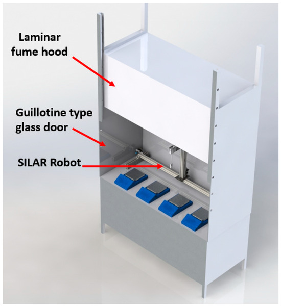
Figure 1.
CAD design of the Fume Hood.
The SILAR robot was developed to achieve precise linear movements along the X-axis and Y-axis, with a displacement of 1200 mm on the X-axis and 200 mm on the Y-axis. These movements allow controlled and accurate substrate immersion into cationic, anionic, and rinse solutions, ensuring uniform thin-film deposition (Figure 2). Figure 3 presents the substrate holder, which was designed to accommodate a variety of substrate materials, including glass, Kapton polyimide, and PET, as well as films of different sizes intended for deposition.
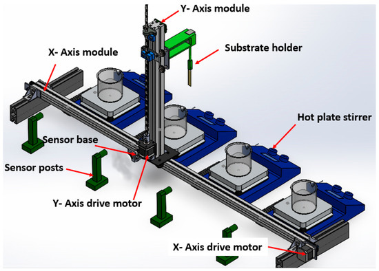
Figure 2.
CAD design of the SILAR robot.
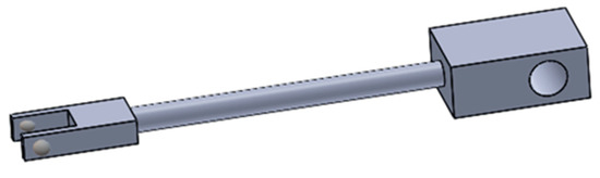
Figure 3.
CAD design of the substrate holder.
The SILAR machine was assembled using the OPENBUILDS modular V-Slot system for both the X-axis and Y-axis. This material was selected due to its high rigidity, ensuring stability during movement. The machine design is divided into two main sections. The first section corresponds to the X-axis, which consists of a Nema 17 stepper motor 17HS4401 (StepperOnline, China that enables horizontal sliding, supported by a pulley and a GT2 timing belt. The second section corresponds to the Y-axis, which carries a substrate holder designed as a 3D robotic arm. This axis performs vertical movement using another Nema 17 stepper motor and an iron shaft. The Y-axis module is mounted onto the X-axis structure, allowing for combined horizontal and vertical motion. The robotic arm is specifically designed to securely hold various types of substrates while maintaining a 90° orientation during all movements. To enhance safety, sensors were integrated to continuously monitor the arm’s position and prevent potential collisions. Given that the thin-film manufacturing process involves the handling of chemical solutions, the robot operates inside a fume hood. The fume hood is entirely constructed from aluminum and is equipped with an industrial extractor motor to ensure effective removal of vapors and gases. Additionally, it features a glass door that allows for a clear observation of the process without interrupting the operation. Figure 4a shows the fully assembled SILAR robot, and Figure 4b shows the fume hood setup used during the experiments.
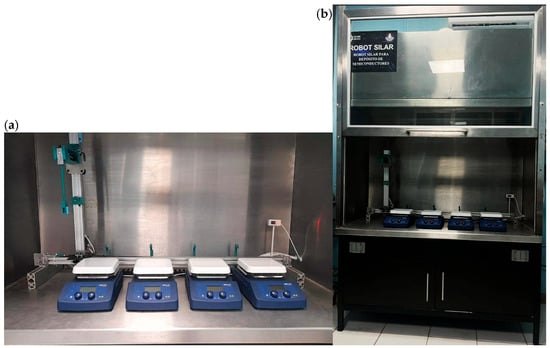
Figure 4.
(a) Final assembly of the SILAR robot. (b) Final installation of the fume hood.
For safety reasons, the control panel is equipped with an emergency stop button that immediately disables the entire system if needed. Additionally, it includes an LED button that not only initiates the process but also indicates when the robot is in operation (Figure 5). Furthermore, the X-axis is equipped with a micro switch at its endpoint, serving as an additional safety mechanism. When triggered, the micro switch immediately stops the robot, indicating that the X-axis has exceeded its designated travel range. Additionally, the control panel includes a four-digit display that shows the current deposition cycle, allowing for a real-time monitoring of the process.
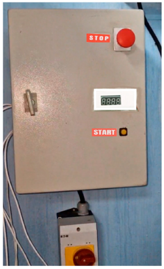
Figure 5.
Control panel surface.
2.2. Electrical and Electronic Circuitry
The system is powered by two main supplies: a 12 V DC, 10 A source dedicated to the stepper motors and their controllers, ensuring precise linear movements along the X- and Y-axes; and a 5 V DC, 5 A supply that powers the electronic components, including sensors, micro switches, the touchscreen interface, and the main controller. Specific drivers for the Nema 17 motors are installed to optimize motor control, along with two circuit breakers that protect the electrical circuits. An industrial-grade switch is included to ensure safe startup and shutdown of the system. A Raspberry Pi Pico microcontroller RP2040 (Raspberry Pi, Reino Unido) manages the overall process, as illustrated in Figure 6.
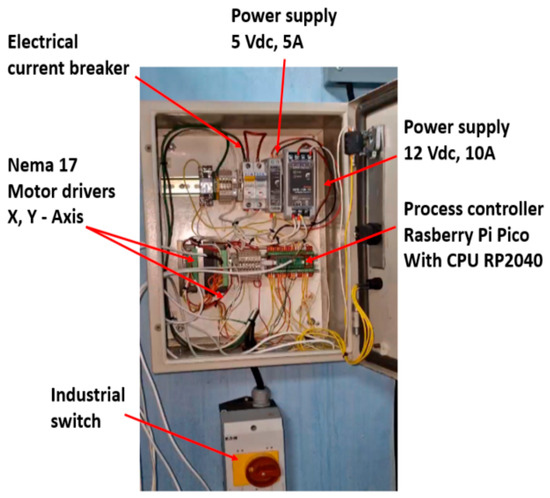
Figure 6.
Electrical schematic diagram of the SILAR robot, showing the power distribution, motor controllers, sensors, and microcontroller connections.
The electrical system operates from a 127 V AC input, which is converted to direct current (DC) using dedicated power supplies. The microcontroller functions at 5 V for its core operations and at 3.3 V for digital communication with peripherals. Communication between system components, such as motors and sensors, is managed through digital and PWM signals, enabling precise and coordinated control. This system architecture is illustrated in Figure 7a. Figure 7b presents the connection diagram of the SILAR robot control system, detailing the layout of components and their integration with the Raspberry Pi Pico board. It includes the controllers and motors for the X- and Y-axes, limit switches (Switches 1, 2, 3, and 4), a line follower sensor (used as a station detector), and a 7-segment display for cycle visualization. The diagram also shows the power supply arrangement, which uses 12 V and 5 V sources protected by a thermal magnetic switch and fuses. The connections are organized to ensure proper operation, safety, and seamless interaction between the motors, sensors, and the control unit, ultimately enabling efficient and reliable system performance.
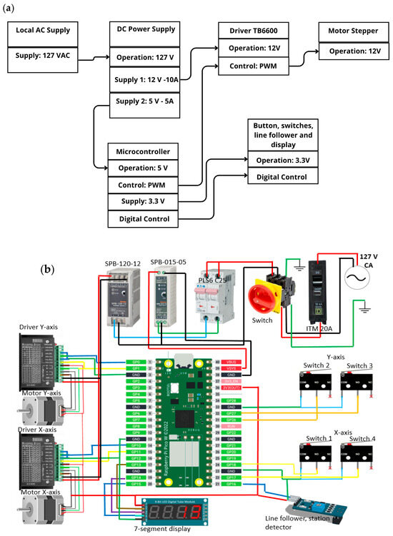
Figure 7.
(a) Power and control block diagram. (b) Connection diagram of the elements used with the Raspberry Pi Pico.
2.3. Automation and Communication Between the Interface and the System
The SILAR robot prototype employs a Raspberry Pi Pico microcontroller, powered by an RP2040 CPU, as its main controller. The microcontroller is programmed using Python (Thonny 4.0.2) and manages key functions, including the precise control of the robot’s movements along the X- and Y-axes.
- On the X-axis, three main functions are implemented:
- Function 1: Activates the X-axis motor to move the arm to the right until the follower sensor is triggered. Motor speed is precisely controlled using a PWM signal previously defined in the program.
- Function 2: Moves the arm slightly to deactivate the follower sensor, allowing Function 1 to be executed again. The motor is activated for 1 s and then automatically deactivated.
- Function 3: Moves the arm leftward to return it to the starting (home) position. The motor continues running until the X-axis micro switch is triggered, signaling the system to stop the movement.
- On the Y-axis, the following functions are implemented:
- Function 1: Activates the motor to move the arm downward for submersion. The motor continues running until the lower micro switch is triggered, at which point it stops automatically. Then a timer starts to record the submersion duration.
- Function 2: Activates the motor to move the arm upward, returning it to the initial position. The motor stops once the upper micro switch is triggered.
These functions operate within two nested loops: the first loop determines the number of stations, while the second loop sets the cycle count, dictating the repetitions for the station loop based on the total number of cycles. Figure 8 illustrates the programming flowchart of the SILAR robot, which follows this sequence. The SILAR process involves immersing substrates in four vessels containing cationic, wash, and anionic solutions. The key parameters of this process include the number of cycles and the immersion duration for each vessel. Users input these parameters through a touchscreen interface. The microcontroller facilitates communication between the interface and the system, ensuring that each actuator precisely positions the substrate in the respective vessel and controls the immersion time.
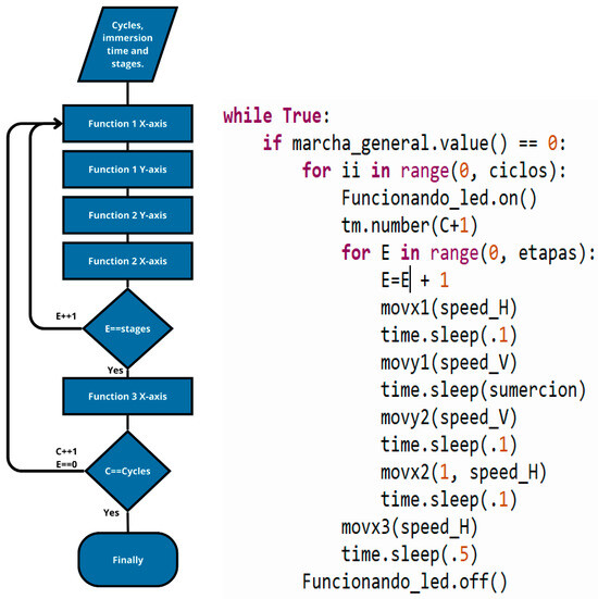
Figure 8.
Programming flowchart of the SILAR robot.
2.4. Deposition and Characterization of CZTS Thin Film
2.4.1. Substrate Cleaning
In this work, CZTS thin films were deposited onto borosilicate glass substrates measuring 25 mm × 76 mm × 1 mm. Prior to deposition, the substrates underwent a single-step cleaning process using a neutral detergent, followed by rinsing with water. Subsequently, the substrates were immersed and agitated in a distilled water, acetone, and isopropyl alcohol solution using ultrasonication for 10 min. Finally, the substrates were dried with a nitrogen gas flow.
2.4.2. Deposition of CZTS Thin Film
The cationic precursor solution (Cu+, Zn+, Sn+) was prepared by dissolving 0.015 M CuCl2, 0.075 M ZnSO4, and 0.01 M SnCl2 salts in 175 mL of deionized water in the first beaker. The anionic precursor (S−) was prepared separately by dissolving 0.15 M Na2S in 175 mL of deionized water. Additionally, two rinsing beakers were filled with 175 mL of deionized water each. All solutions were stirred on a hot plate for 10 min to ensure complete dissolution. Table 1 presents the deposition parameters, including the dipping time in each solution and rinsing step, the number of cycles, dipping and rinsing temperatures, and the horizontal axis speed. The total deposition time varied according to the immersion time and the number of deposition cycles.

Table 1.
Parameter controlled by the SILAR process.
The substrates were set in the holder, and the vertical and horizontal axes were positioned at the origin. The deposition parameters were transmitted via serial communication to the microcontroller; once correctly received, the SILAR process started. Each cycle involved the adsorption and reaction of cationic and anionic precursors, alternated with rinsing steps in a separate beaker. Upon completion of the deposition cycles, the films were subjected to optical and structural characterization. Subsequently, the films were annealed in an N2 atmosphere at 350 °C for 20 min. For structural analysis, X-ray diffraction (XRD) was conducted using a Rigaku D/MAX 2200 diffractometer with monochromatized CuKα radiation (λ = 1.54056 Å). Measurements were performed over a ω–2θ range of 20°–80°, employing a grazing incidence angle of 1° to enhance surface sensitivity. Additionally, Raman spectroscopy was employed to complement the structural analysis. Raman spectra were recorded with a Horiba Jobin Yvon micro-Raman system coupled to an Olympus BX41 microscope, using a He–Ne laser source (λ = 632 nm, 20 mW power). Together, these techniques provided a comprehensive understanding of the crystalline structure and phase composition of the deposited CZTS films.
3. Results
Figure 9 presents a series of CZTS films deposited with 10-cycle increments between samples, allowing the observation of progressive changes in their appearance. After 20 cycles, the surface exhibits a light brown color, which progressively darkens as the number of cycles increases up to 60. This gradual color change indicates continuous material accumulation, suggesting an increase in film thickness or density with each additional deposition cycle.
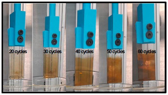
Figure 9.
Surface color of CZTS thin films: SLG/CZT.
Table 2 presents the thickness values of the films deposited after 40 cycles. These measurements were obtained using the double weighing method. This method involves measuring the mass of the substrate before and after deposition, considering only the effective deposition area, which in this case is 8 cm2. Based on these measurements, the following equation was applied to calculate the film thickness.
where the density depends on the substrate used.
Table 2.
Thickness of the deposited films after 40 cycles.
An optical characterization of the sample deposited with 40 cycles was carried out after deposition and annealing under the conditions listed in Table 1. The optical properties of the films were evaluated by measuring their reflectance and transmittance using an Ocean Optics USB4000 UV-Vis spectrometer. The energy band gap of the CZTS thin film was estimated from the diffuse transmittance data using the Kubelka–Munk function, as described by the following equation [14].
where K is the absorption coefficient given by , S is the scattering factor given by , is the photon energy given by , and is the reflectance (%).
The absorption coefficient α was estimated from the Transmission (T) data using the following relation [15,16]:
where R is the reflectance given by R = 1 − T, and d is the film thickness.
Figure 10 shows the estimated bandgap of the A1 thin film, which is 1.34 eV, close to the optimal range (~1.45 eV) for high-efficiency solar cell applications. In contrast, the absorption coefficient ranges from 6 × 10³ to 1 × 104 cm−1 across the photon energy range of 1.2 to 2.7 eV. This suggests that a greater film thickness may be required to achieve sufficient light absorption (~1 µm).
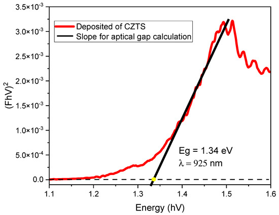
Figure 10.
Band gap estimation for the CZTS thin film at 40 cycles.
The structural characterization of the CZTS thin films was carried out using X-ray diffraction (XRD) to verify their crystalline structure and phase composition. The XRD pattern of sample A1a is presented in Figure 11. An amorphous background is observed between 20° and 33°, indicating the presence of a partially disordered phase. However, prominent diffraction peaks corresponding to the kesterite structure of CZTS are visible, in accordance with the Joint Committee on Powder Diffraction Standards (JCPDS) file 00-024-0061. Specifically, the peaks located at 28.5°, 32.9°, 47.4°, and 56.2° are indexed to the (111), (200), (220), and (311) planes, respectively, confirming the successful formation of the CZTS crystalline phase. Raman spectroscopy was employed as a complementary technique. Figure 12 presents the Raman spectra of the samples. The as-deposited films exhibited Raman modes associated with SnS, CZTS [12,13,14], Cu2−xS [17,18,19], and SnS2 phases. After thermal annealing at 350 °C for 20 min, the SnS2 phase was notably suppressed, improving the film quality. A Raman peak detected at 148 cm−1 is attributed to SnS, suggesting the possible presence of complex phase compositions or decomposition products at elevated annealing temperatures [20]. Furthermore, following Chaudhari JJ et al., the peak observed at 336 cm−1 is assigned to the A1 vibrational mode, which is related to the oscillations of sulfur atoms within the CZTS lattice [21].
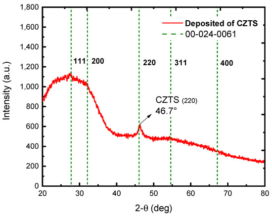
Figure 11.
X-ray diffraction (XRD) pattern of the CZTS thin film deposited on a substrate, showing the characteristic peaks associated with the kesterite crystalline structure.
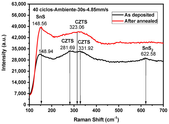
Figure 12.
Raman spectrum of CZTS thin film at 40 cycles.
Figure 13 shows scanning electron microscopy (SEM) micrographs of the CZTS samples. Both images were acquired at an accelerating voltage of 1.0 kV, a working distance (WD) of 7.7 mm, and a scale of 100 nm. The micrographs reveal a highly porous and rough surface morphology, characterized by nanometric agglomerated particles forming a dense and compact network. The surface displays regions with a high material concentration alongside areas with lower accumulation, indicating a heterogeneous morphological distribution across the sample.
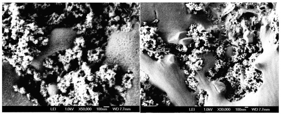
Figure 13.
SEM of A1a CZTS thin film.
For a more complete view of the CZTS deposits by the developed SILAR machine, please refer to the authors’ previous work at https://doi.org/10.3390/nano15020085. In this study, complementary analyses were presented, including optical, structural, morphological, and chemical characterizations performed before and after annealing, which support the improvement in crystallinity, the reduction of secondary phases, and the optimization of the material’s optical properties after heat treatment [22].
4. Conclusions
Automating the SILAR deposition process using a Raspberry Pi Pico microcontroller demonstrated a reliable and efficient method for controlling the deposition conditions of CZTS thin films. The system provided precise control of cycles, immersion times, and substrate positioning, enabling uniform and reproducible film deposition. Automation reduced manual intervention and enhanced process safety, repeatability, and deposition accuracy through fine-tuned control of key parameters. Optical and structural characterizations confirmed the successful formation of CZTS thin films, with an estimated bandgap of 1.34 eV, suitable for photovoltaic applications. Although XRD analysis indicated a largely amorphous structure, Raman spectroscopy revealed the presence of secondary phases, such as SnS, Cu2−XS, and SnO2. Morphological analysis revealed a highly porous and rough surface, composed of agglomerated nanometric particles forming a compact network. The heterogeneity in material distribution at the nanoscale suggests localized variations during the growth process, which could influence the optical and electronic behavior of the films. These results validate the effectiveness of the automated SILAR system for producing CZTS thin films and highlight its potential, cost-effective strategy for the development of solar cells and other semiconductor-based electronic devices.
Author Contributions
Conceptualization, P.J.V.-G. and C.A.H.-G.; methodology, C.A.H.-G.; software, P.J.V.-G., C.A.H.-G., M.L.P.-C., and R.M.-G.; validation, P.J.V.-G., C.A.H.-G., M.L.P.-C., and R.M.-G.; formal analysis, P.J.V.-G., C.A.H.-G.; investigation, P.J.V.-G., C.A.H.-G., M.L.P.-C. and R.M.-G.; resources, C.A.H.-G.; data curation, P.J.V.-G., C.A.H.-G., M.L.P.-C., and R.M.-G.; writing—original draft preparation, P.J.V.-G., C.A.H.-G., M.L.P.-C., and R.M.-G.; writing—review and editing, C.A.H.-G.; visualization, M.L.P.-C.; supervision, R.M.-G.; project administration, C.A.H.-G.; funding acquisition, C.A.H.-G. All authors have read and agreed to the published version of the manuscript.
Funding
This research received no external funding.
Institutional Review Board Statement
Not applicable.
Informed Consent Statement
Not applicable.
Data Availability Statement
The data are contained within the article.
Acknowledgments
To A. Meza-Avendaño for assistance in operating the UV-Vis spectrophotometer and XRD.
Conflicts of Interest
The authors declare no conflicts of interest.
References
- Capitaine, J.A.C. Automation of Carbon Nanostructure Synthesis by the Ultrasonic Spray Pyrolysis Method. Master’s Thesis, Monterrey Institute of Technology and Higher Education, Monterrey, Mexico, 2022. Available online: https://hdl.handle.net/11285/651117 (accessed on 20 June 2025).
- Muñoz, B.C.; Hernández Bedoya, S.F. Automation and Control of an Aerosol-Assisted Chemical Vapor Deposition (AACVD) System Using an Arduino Programming Board and Precision Sensors [Ponencia, Universidad Tecnológica de Pereira]. Universidad Tecnológica de Pereira. Available online: https://media.utp.edu.co/vicerrectoria-de-investigaciones/archivos/PONENCIA%20-%20ESTUDIO%20DE%20MATERIALES%20Y%20DESARROLLO%20DE%20TECNOLOGIAS%20PARA%20CALENTAMIENTO%20SOLAR.pdf (accessed on 20 June 2025).
- Reynoso, E.A.J.; Chávez-Cervantes, N.; Talamantes-Nieto, B. Automated fabrication of compact thin films in the development of Grätzel-type solar cells. J. Technol. Innov. 2017, 4, 36–42. [Google Scholar]
- Soonmin, H. Recent Advances in the Growth and Characterizations of SILAR-Deposited Thin Films. Appl. Sci. 2022, 12, 8184. [Google Scholar] [CrossRef]
- Gao, X.; Wang, X.Y. Synthesis and optical properties of ZnO nanocluster porous films deposited. Appl. Surf. Sci. 2004, 229, 275–281. [Google Scholar] [CrossRef]
- Altieri, W.M.; Sadafi, R.; Felix, S.; Boulfrad, S.; Lopes, R.; Prodanovic, S.; Kalantari, K.; Spanos, S.; Doeblinger, M.; Lichon, C.; et al. Development of an automated SILAR method for the sustainable fabrication of BiOI/TiO2 photoanodes. Energy Adv. 2024, 3, 2564–2574. [Google Scholar] [CrossRef] [PubMed]
- Valdez Martínez, J.; Martínez, M.A.; Camacho-Rangel, M.; Rodríguez, M.J.; Baca-Escobar, M.; Villarreal, T.J.; Baca-Escobar, B.E. Automation of the successive ionic layer adsorption and reaction (SILAR) process. Rev. Mex. Ing. Química 2020, 19, 1351–1361. [Google Scholar] [CrossRef]
- Azpeitia, H.J.; Martínez, M. Sistema de transporte para la deposición de películas de materiales iónicos por inmersión y método de operación. Jóvenes Investig. 2016, 1, 42–46. [Google Scholar]
- Suryawanshi, M.P.; Shin, S.W.; Ghorpade, U.V.; Gurav, K.V.; Hong, C.W.; Patil, P.S.; Moholkar, A.V.; Kim, J.H. Improved solar cell performance of Cu2ZnSnS4 (CZTS) thin films prepared by sulfurizing stacked precursor thin films via SILAR method. J. Alloys Compd. 2016, 671, 509–516. [Google Scholar] [CrossRef]
- Kaza, J.; Pasumarthi, M.R.; Avadhani, P.S. Superstrate and substrate thin film configuration of CdS/CZTS solar cell fabricated using SILAR method. Opt. Laser Technol. 2020, 131, 106413. [Google Scholar] [CrossRef]
- Kumar, K.G.; Bhargav, P.B.; Prakash, D.G.; Kaushik, R.; Mathew, E.R.; Shriram, M.K.; Veerathangam, K. Investigations on SILAR coated CZTS thin films for solar cells applications. Phase Transit. 2021, 94, 556–566. [Google Scholar] [CrossRef]
- Garzón Ramos, D.; Martínez, M.A.; Rodríguez, D.; Guzmán, G.D.; Castro, V. Sistema SILAR de producción para películas semiconductoras aplicadas en sensores de humedad. In Proceedings of the 16 Convención Científica de Ingeniería y Arquitectura, Havana, Cuba, 26–30 November 2012. [Google Scholar]
- Sen Gupta, A.K.; Adnan, A.; Bhattacharjee, S.; Das, N.K.; Matin, M.A.; Quamruzzaman, M. SnapFib: An Easy Build Arduino-based Tabletop Prototype for Thin Film Deposition by Successive Ionic Layer Adsorption and Reaction Method. Mendeley Data, V4. 2022. Available online: https://data.mendeley.com/datasets/3pccd4yp8m/4 (accessed on 20 June 2025).
- Júnior, S.L.; Segundo, I.R.; Freitas, E.; Vasilevskiy, M.; Carneiro, J.O.; Tavares, C.J.M. Use and misuse of the Kubelka-Munk function to obtain the band gap energy from diffuse reflectance measurements. Solid State Commun. 2022, 341, 114573. [Google Scholar]
- Chamekh, S.; Khemiri, N.; Kanzari, M. Effect of annealing under different atmospheres of CZTS thin films as absorber layer for solar cell application. SN Appl. Sci. 2020, 2, 1507. [Google Scholar] [CrossRef]
- Touati, R.; Rabeh, M.B.; Kanzari, M. Effect of post-sulfurization on the structural and optical properties of Cu2ZnSnS4 thin films deposited by vacuum evaporation method. Thin Solid Film. 2015, 582, 198–202. [Google Scholar] [CrossRef]
- Lakhe, M.G.; Bhand, G.; Rohom, A.; Londhe, P. Electrochemical Synthesis and Characterization of Cu2ZnSnS4 Thin Films. J. Mater. Sci. Eng. 2016, 5, 1000261. [Google Scholar] [CrossRef]
- Suryawanshi, M.P.; Shin, S.W.; Ghorpade, U.V.; Gurav, K.V.; Hong, C.W.; Agawane, G.L.; Vanalakar, S.A.; Moon, J.H.; Yun, J.H.; Patil, P.S.; et al. Moholkar, Improved photoelectrochemical performance of Cu2ZnSnS4 (CZTS) thin films prepared using modified successive ionic layer adsorption and reaction (SILAR) sequence. Electrochim. Acta 2014, 150, 136–145. [Google Scholar] [CrossRef]
- Buldu, D.G.; Cantaş, A.; Turkoglu, F.; Akca, F.; Meriç, E.; Özdemir, K.M.; Tarhan, E.; Ozyuzer, L.; Aygun, G. Influence of sulfurization temperature on Cu2ZnSnS4 absorber layer on flexible titanium substrates for thin film solar cells. Phys. Scr. 2018, 93, 024002. [Google Scholar] [CrossRef]
- Zhang, X.; Fu, E.; Zheng, M.; Wang, Y. Fabrication of Cu2ZnSnS4 Thin Films from Ball-Milled Nanoparticle inks under Various Annealing Temperatures. Nanomaterials 2019, 9, 1615. [Google Scholar] [CrossRef] [PubMed]
- Chaudhari, J.J.; Joshi, U.S. Optimization of Cu2ZnSnS4 thin film absorber layer growth without sulphurization using triethanolamine as complexing agent for thin film solar cells applications. J. Mater. Sci. Mater. Electron. 2018, 29, 7048–7056. [Google Scholar] [CrossRef]
- Vázquez-González, P.J.; Paniagua-Chávez, M.L.; Zebadua-Chavarria, L.A.; Mota-Grajales, R.; Meza-Avendaño, C.A.; Campos-González, E.; Escobosa-Echavarría, A.; Hu, Y.; Pérez-Ramos, A.E.; Manuel-Matuz; et al. Comprehensive Structural, Chemical, and Optical Characterization of Cu2ZnSnS4 Films on Kapton Using the Automated Successive Ionic Layer Adsorption and Reaction Method. Nanomaterials 2025, 15, 85. [Google Scholar] [CrossRef] [PubMed]
Disclaimer/Publisher’s Note: The statements, opinions and data contained in all publications are solely those of the individual author(s) and contributor(s) and not of MDPI and/or the editor(s). MDPI and/or the editor(s) disclaim responsibility for any injury to people or property resulting from any ideas, methods, instructions or products referred to in the content. |
© 2025 by the authors. Licensee MDPI, Basel, Switzerland. This article is an open access article distributed under the terms and conditions of the Creative Commons Attribution (CC BY) license (https://creativecommons.org/licenses/by/4.0/).