Article

Chemical Synthesis of Nanostructured Topological Pb1−xSnxSe (x = 0–1) Alloy Films—A Study of Their Structural, Optical, and Thermopower Properties

by
Esteban Díaz-Torres
1,*,
Ángel Guillén-Cervantes
2 and
Mauricio Ortega-López
1,*
1
Sección de Electrónica del Estado Sólido, Departamento de Ingeniería Eléctrica, Centro de Investigación y de Estudios Avanzados del Instituto Politécnico Nacional, Av. Instituto Politécnico Nacional, No. 2508, Ciudad de México 07360, Mexico
2
Departamento de Física, Centro de Investigación y de Estudios Avanzados del Instituto Politécnico Nacional, Av. Instituto Politécnico Nacional, No. 2508, Ciudad de México 07360, Mexico
*
Authors to whom correspondence should be addressed.
Micro 2025, 5(1), 13; https://doi.org/10.3390/micro5010013
Submission received: 28 December 2024 / Revised: 3 March 2025 / Accepted: 13 March 2025 / Published: 16 March 2025
(This article belongs to the Special Issue Advances in Micro- and Nanomaterials: Synthesis and Applications)

Abstract

:
The spray pyrolysis deposition of nanostructured Pb1−xSnxSe alloy films, x = 0.0 to 1.0, from as-prepared Pb1−xSnxSe alloy colloids as the starting solution is reported. The colloidal dispersions were prepared by dissolving selenium in an amine–thiol mixture, reacted with the Sn and Pb precursors in propylene glycol, and subsequently sprayed onto glass substrates at 300 °C. Structural characterization indicated the formation of the alloyed rock-salt cubic phase for 0.0 ≤ x ≤ 0.75, oxidized Pb and Se phases produced during the deposition, and only orthorhombic SnSe for x = 1.0 with Se and SnSe2 as impurities. Nanocrystalline films ranging from 16 to 16.5 nm in size were obtained. The films displayed a shift in their optical structure and a non-monotonic variation in the band gap energy, first a decrease, reaching the minimum at x = 0.30 and a further increase in the Sn content. The decrease in the optical band gap resembles that of a topological insulator behavior. The morphology of the alloyed films confirmed the large nanocrystal formation by self-assembly processes in both the PbSe and SnSe phases and segregated PbSnSe platelets for x ≥ 0.30. Seebeck coefficient revealed that a typical semiconductor behavior dominated by bipolar transport, and p-type conductivity, but only for x = 0.0 n-type conductivity was exhibited. The maximal Seebeck coefficient magnitude behaved similarly to the band gap energy, evidencing the influence of energy band structure and the topological character.

1. Introduction

Nowadays, thermoelectric materials have allowed power generation and refrigeration applications based on the direct conversion of heat to electricity and conversely. The scientific interest in the quantum confinement effects has attracted great attention since the development of nanostructured materials. The transport mechanisms are of crucial relevance for a deeper understanding of how these materials behave from the electrical, optical, and thermal points of view. In this sense, nanostructured semiconductors hold promises for controlling the electrical and thermal transport separately and consequently to develop high-efficiency thermoelectric devices [1].
PbSe has a positive temperature coefficient, direct narrow band gap energy of 0.28 eV at 300 K, relatively large Bohr exciton radius of 46 nm, and it crystallizes into the face-centered cubic structure with a lattice parameter of 6.121 Å. It has also been reported that PbSe can display either n- or p-type conductivity, depending on the type of point defect generated in its crystalline structure [2]. Instead, SnSe exhibits an indirect band gap of 0.90 eV at room temperature, crystallizes into an orthorhombic structure (a = 11.498 Å, b = 4.153 Å, c = 4.440 Å), and displays metallic surface states protected by crystalline symmetry, like a topological crystalline insulator [3]. Also, SnSe always exhibits p-type conductivity due to electrically active tin vacancies.
Solid solutions of the binaries PbSe and SnSe can be only obtained either for 0.0 < x < 0.30 at 300 K (miscibility range) or for 0.0 < x < 0.18 at 77 K with a face-centered cubic structure, producing a decreasing band gap energy at the L point of the Brillouin zone with the composition, contrary to what would be expected from Vegard law [4]. Around x = 0.30, the band gap is closed and for higher Sn contents Eg opens again with marked SnSe phase segregation. In addition, the x > 0.30 alloys preserve these topological crystalline insulator properties from SnSe, which leads to enhanced performance, detailed study of topological insulator properties, and control of the electrical conductivity type [5]. The formation of solid solutions has become an effective method to enhance the ZT figure of merit, for the specific case of PbSe-SnSe solid solutions, where the interaction between the conduction and valence bands (inversion of bands and enabling surface states) is altered by the composition x, making of Pb1−xSnxSe alloys a promising material for the development of new energy conversion devices [4,5,6].
Pb1−xSnxSe alloys have been mainly synthesized by physical techniques, like solid-state reactions of elemental precursors at high temperatures [7,8], self-selecting vapor growth [4], epitaxial deposition by evaporation and MBE [9,10,11], ball-milling [6], and vapor phase transport [12]. As for the chemical synthesis, few efforts have been devoted, for instance, co-deposition in aqueous bath [13] and powder synthesis of the extremes (PbSe and SnSe) in solution [14], being these chemical methods an effective, facile, and cheap way of producing nanocrystalline semiconductor materials with striking morphologies and enhanced properties that greatly differ from their bulk versions. Nevertheless, vapor phase transport, melting, and hydrothermal and solvothermal synthesis routes have proven their potential to produce nanocrystalline chalcogen alloys as well [12,15,16]. PbSe, SnSe, and their alloys have found applications in laser diodes [17,18], detection in the mid-IR range [19,20], and thermoelectricity [6,21,22,23].
In this work, we report the synthesis and deposition in polyol medium, as well as the structural, optical, morphological, and Seebeck coefficient characterization of sprayed nanostructured Pb1−xSnxSe x = 0.0–1.0 alloy films. It is important to note that we have no knowledge related to the synthesis of these alloys as a colloid and their further deposition as a film by spray pyrolysis in a combined way. However, to the best of our knowledge, there is only one report in the literature on the deposition of PbSe/PbSnSe heterostructures [24], following a similar procedure as that reported herein.

2. Materials and Methods

Pb1−xSnxSe alloys were chemically synthesized by the universal solvent method (alkahest) [25] in polyol medium, using selenium powder (Se, 99.5% purity), triethanolamine (TEA, 98% purity), thioglycolic acid (TGA, 99% purity), polyvinylpyrrolidone (PVP), propylene glycol (PG, 99% purity), tin chloride (SnCl2, 98% purity), and lead nitrate (Pb(NO3)2, 99% purity). All the reactants were purchased from Sigma-Aldrich, Toluca, Mexico Meyer, Ciudad de Mexico, Mexico and Fluka, Buchs, Switzerland and used without further purification.

2.1. Synthesis and Deposition

The precursor solutions were prepared as follows: By mixing 1.5 mmol of selenium powder and 1.35 mL of triethanolamine under magnetic stirring. After 5 min, 0.15 mL of thioglycolic acid was added, followed by 0.1 g PVP, and 5 min later 20 mL of propylene glycol to disperse. The nominal molar fraction x = [Sn]/([Sn] + [Pb]) was varied: x = 0.0, 0.05, 0.15, 0.30, 0.50, 0.75, and 1.0, always maintaining [Sn] + [Pb] = 1.5 mmol, by dissolving separately SnCl2 and Pb(NO3)2 in 5 mL of propylene glycol and heated up to 80 °C. First, when the selenium solution reached 120 °C, the tin precursor was added, and the reaction was kept at that temperature for 45 min. Then, the lead precursor was added and the temperature was increased up to 180 °C and kept for 3 h. For the extreme cases, x = 0.0 and 1.0, once 120 °C was reached in the selenium solution, either the lead or tin precursor was added immediately to the selenium solution and the temperature was increased up to 180 °C. Finally, the colloidal dispersion was cooled to room temperature and an additional 30 mL of propylene glycol was added for its processing as a film.
The deposition procedure by the spray pyrolysis is indicated in a previous publication [26], but here we used 10 mL of the as-prepared alloy colloid mixed with 10 mL of propylene glycol and 10 mL of deionized water, at 300 °C of deposition temperature. Two deposits were performed, one on Corning glass substrates treated in piranha solution and sonication, and the other one on ITO-covered glass substrates cleaned with acetone and 2-propanol in sonication and dried all at 80 °C. The deposits on ITO/glass enabled thermopower characterization, masking the considerable Seebeck contribution from the glass, which is an insulator. The substrate effect on Seebeck coefficient measurements in the films is shown in the Supplementary Materials.

2.2. Sample Characterization

The phase composition and structure were assessed by X-ray diffraction (XRD) by a PANalytical XPERT-PRO diffractometer (Malvern Panalytical, Malvern, UK), Cu-Kα emission line, with a 0.04° step in the range of 20–60°. Morphological characterization was performed, using a field emission-scanning electron microscope (FE-SEM) Zeiss-Auriga 39-16 (Carl Zeiss Microscopy GmbH, Jena, Germany) and a JEOL JSM 7401F (JEOL Ltd., Peabody, MA, USA), operating at 1 and 2 kV, respectively. Optical characterization was carried out with a Jasco V-670 spectrophotometer (JASCO Inc, Easton, MD, USA) in the spectral absorption mode for the 400 to 2000 nm wavelength range and 1 nm resolution. Seebeck coefficient measurements in the 300–423 K temperature range were performed with homemade equipment based on the differential method [27]. Each film was placed onto two metal heater plates and then two K-type thermocouples were placed onto the film to register both the thermo-voltage and temperature simultaneously. A Keithley 228A power supply injects a constant current of 260 mA to produce an uneven temperature increase in the heaters. The data were acquired by a Keithley 6517B electrometer (Keithley Instruments Inc, Solon, OH, USA) and a NI USB-9219 A/D converter-amplifier (National Instruments Corporation, Austin, TX, USA). These instruments were interfaced by a computer program in LABVIEW (National Instruments Corporation, TX, USA), which also calculates the Seebeck coefficient.

3. Results and Discussion

3.1. Structural and Composition Results

Figure 1 shows the XRD patterns for both as-deposited alloy films and their extremes, PbSe and SnSe. Films well-crystallized in the face-centered cubic structure (rock-salt) were obtained for x = 0.0–0.75 and in the orthorhombic structure for x = 1.0 (Figure 1a). The diffraction peaks were indexed using the ICDD 00-006-0354 reference card of PbSe (vertical continuous lines and blue indices). By increasing the Sn content of each alloy, the diffraction peaks (111), (200), and (220) were broadened from their right-hand side and deformed for x ≥ 0.50. Such deformations were assumed to be peaks of the SnSe phase emerging from the PbSe lattice (doublet), but their indexing with the ICDD 00-048-1224 reference card of orthorhombic SnSe did not match. The ICDD 01-089-4781 card belonging to the SnSe rock-salt cubic phase was proven, matching with the emergent peaks (in agreement with vertical dashed lines and blue indices).
The presence of the SnSe cubic phase is consistent with the (3D) alloyed PbSnSe phase [10], suggesting the incorporation and alloying of high tin content and preservation of the cubic phase even for x = 0.75. However, the SnSe cubic phase is unstable under normal pressure and temperature conditions, so it is reasonable to consider some deformation in the crystal structure from the layered SnSe orthorhombic phase to be like a cubic one.
The colloidal route used leads to the secondary phases-free nanocrystal formation, but the presence of oxidized impurity traces is only manifested after the deposition, like PbO•xH2O SeO2, PbSeO3, and PbSeO4, for x between 0.05 and 0.50, which were significantly reduced for x = 0.75. Nevertheless, it is important to note that the starting materials have a slightly low purity (SnCl2 98% and Pb(NO3)2 99%), resulting in the presence of impurities in very low concentrations in the films, which were not detected by X-ray diffraction but cannot be ruled out. Hence, it is assumed that the effects of the impurities from the starting materials are minimal.
As for x = 1.0 (SnSe), the results indicated that the high-intensity peaks could be indexed to the SnSe orthorhombic phase, according to the ICDD 00-048-1224 reference card (vertical dotted lines and red indices). Additionally, secondary phases were also crystallized and appeared in the pattern, mainly SnSe2 and orthorhombic selenium produced even from the colloidal reaction. It was possible to calculate the lattice constants: a = 11.499 Å, b = 4.068 Å, and c = 4.472 Å by the diffraction peaks (111), (400), and (501). The lattice constants a and c exhibited tensile stress of 0.01% and 0.72%, respectively, whereas a very significant compressive stress of 2.05% on the lattice constant b was displayed. From the peaks (410) and (511) the crystal size was estimated by the Scherrer equation [28], resulting in 16.36 nm. In a similar way, using the peaks (111), (200), and (220) the crystal size for x = 0.0 (PbSe) was calculated, obtaining 16.42 nm, which indicates the formation and deposition of nanostructured material. We noted that PbSe and SnSe films consist of nano-sized material, according to XRD data analysis. The patterns revealed that the PbSe peaks are apparently narrow, and it resulted in a 16.42 nm nanocrystalline material, in turn, the peaks of the alloys are broader. This broadening is attributed to both the alloying effect and crystallization of into nano-sized material. It is also important to mention that in the alloys, the only varied parameter was the tin content, suggesting that the crystal size was not significantly impacted for x. Therefore, the alloy films also exhibit a nanocrystalline nature.
On the other hand, the lattice constant a for the cubic phase of PbSe and the alloys was determined from the peaks (311) and (222) located at greater 2θ angles, where the alloying effect is appreciable. Figure 1b displays the lattice constant as a function of the nominal Sn content. For x = 0.0 (PbSe), it resulted in a = 6.111 Å, suggesting that the crystalline lattice of the deposit is compressed by 0.16% concerning the reference value for those peaks. Thus, we can consider that all of the alloyed films and that of SnSe as described above are subjected to stress. As x increased, the lattice constant decreased for each alloy film, varying from 6.111 Å to smaller values, where the decrease continued for x = 0.75. Assuming that the trend would continue, even up to x = 1.0, a minimum lattice constant of 6.042 Å would be obtained, whose value would be close to the 5.990 Å of the corresponding SnSe cubic phase. Hence, Sn incorporated into the PbSe lattice gave rise to a compressed lattice in addition to the compression stress on the pure PbSe lattice. Based on the above, a fit was performed on the lattice constant data by a linear curve (Vegard law equivalent for our alloys), see Equation (1).
a = 6.042 x + 6.108 1 x
This result also suggests that our chemical synthesis procedure produced well-crystallized 3D-Pb1−xSnxSe alloys in the rock-salt phase, even for larger nominal molar fractions, 0.30 ≤ x ≤ 0.75 (extended solubility limit). As mentioned above, pure cubic SnSe is an unstable phase; therefore, a phase transformation of layered orthorhombic SnSe could occur. The orthorhombic SnSe unit cell could be deformed by the presence of Pb atoms and crystallize rotated 45° in regard to the PbSe rock-salt cubic cell, in order to match it [10]. This leads to an equivalent lattice parameter calculated by b 2 + c 2 [29] that resulted in 6.045 Å, using the lattice constants of the SnSe sample indicated above and whose value is very close to 6.042 Å for x = 1.0 (cubic SnSe) obtained from Equation (1). Therefore, it is confirmed that cubic SnSe detected by XRD corresponds with a deformed SnSe layered orthorhombic phase, coexisting with the PbSe phase. In addition, this phase transformation allowed for a higher tin incorporation by alloying, in agreement with our proposed Vegard law.

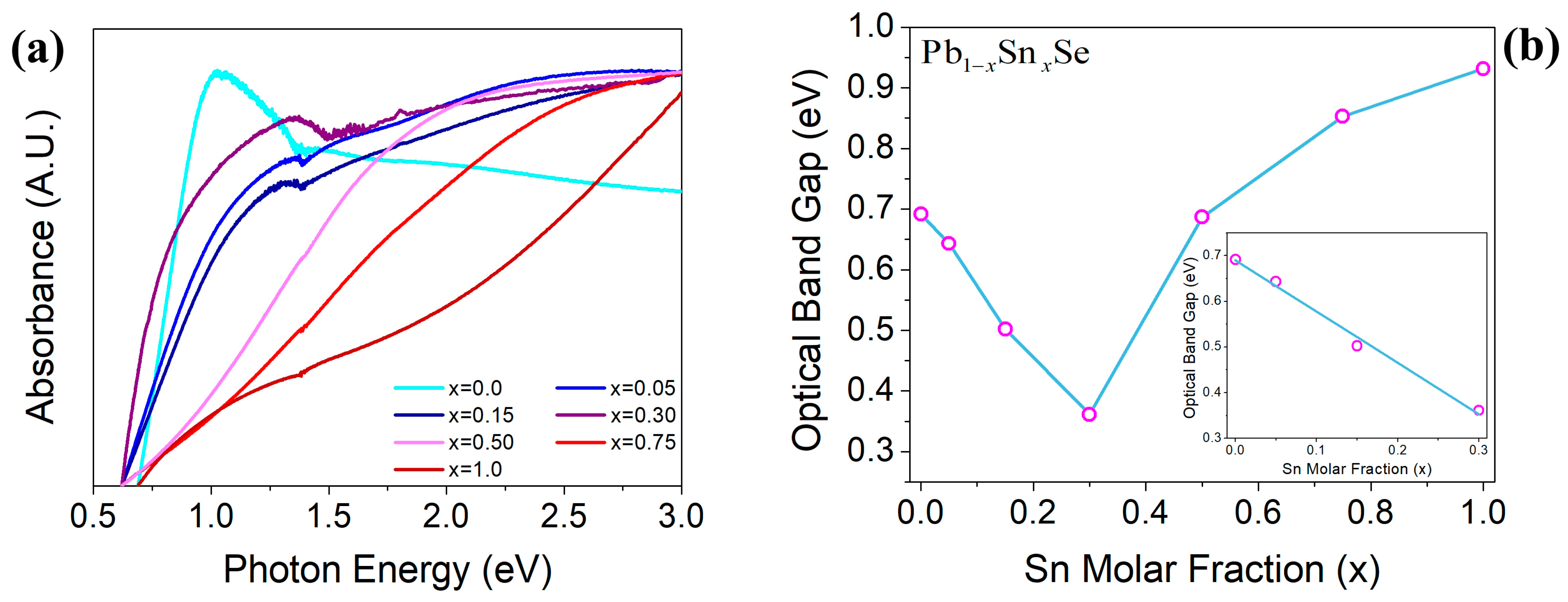
3.2. Optical Properties Results

Absorption spectra as a function of the photon energy for the alloy films and their extremes (Pb1−xSnxSe) are shown in Figure 2a. For x = 0.0 (PbSe), it can be seen that the absorption edge is located at a value less than 0.70 eV. As the Sn content increased, the absorption edge slope changed and was shifted towards lower energies than 0.70 eV up to x = 0.30. Starting from x = 0.50, the slope changed significantly and the absorption edge was shifted again, but towards higher energies. These spectra made it possible to estimate approximately the optical band gap energy (Eg) by the Tauc method, considering the exponent value for direct transitions as 1/2, applied to the alloys 0 ≤ x ≤ 0.30, and the value of 2 for indirect transitions to x ≥ 0.50.
Figure 2b displays the obtained optical band gap energy results as a function of the nominal composition (x). These results confirm what was observed qualitatively in the absorption spectra. From x = 0.0 to x = 0.30, the band gap decreased with increasing Sn content, contrary to what would be expected from Vegard law, where the band gap energy would be increased from 0.28 eV corresponding to PbSe (x = 0.0) to 0.90 eV for SnSe (x = 1.0). For x = 0.50–1.0, the band gap exhibits the opposite behavior, increasing with the Sn molar fraction. The decrease in the band gap energy is a behavior that has already been identified and is characteristic of a topological crystalline insulator [4]. The substitutional tin induces an evolution of the energy band structure, leading to the closure of the forbidden band gap at a certain specific composition and reopening above that composition, with reversed electronic states at the edges of conduction and valence bands. Likewise, Dirac cone-like metallic surface states are formed and cross the forbidden band gap, which are manifested when the inversion of energy bands occurs and are protected by crystalline symmetry.
It was possible to fit a straight line on the band gap energy data between x = 0.0 and x = 0.30, corresponding to the miscible range and where Eg decreased in regard to our PbSe (x = 0.0) sample, inset Figure 2b, resulting in Equation (2).
E g = 1.121 x + 0.690
The above result differs from that of Strauss [9], who proposed the following: E g = 0.890 x + 0.265 at 300 K. The main differences are that the samples analyzed by Strauss were epitaxially deposited bulk films, whereas our films correspond to nanostructured polycrystalline material. In fact, the nanostructuring likely caused the shifting of the optical Eg in PbSe (x = 0.0) towards energies higher than 0.28 eV and, as a consequence, that of the alloys as well. This shifted band gap could be produced by quantum confinement effects, as we previously reported [26,30] since PbSe (x = 0.0) is a material with a large Bohr exciton radius (46 nm), and according to XRD, the crystal size was 16.42 nm, almost three times less than the exciton radius. For SnSe (x = 1.0), no appreciable shifting of the band gap was observed due to nanostructuring (Eg = 0.93 eV) because this material displays confinement effects below 1 nm and our material exhibited an average crystal size similar to PbSe. Therefore, the behavior of decreasing and subsequent increasing of the band gap energy also confirms alloy formation, similarly to the phase composition results observed in XRD, as well as the Pb1−xSnxSe formation with topological crystalline insulator properties.

3.3. Morphology Results

Surface view SEM images for representative Pb1−xSnxSe alloys are displayed in Figure 3. For PbSe (x = 0.0) a morphology composed of semispherical- and faceted-like agglomerated granular crystals and porous formed among agglomerated structures is shown in Figure 3a, varying in size from the reported value from XRD (16.42 nm) to various hundreds of nanometers. Large crystals were formed during the colloidal dispersion deposition by self-assembly, from a nanocrystal distribution centered at 16.42 nm as primary building blocks [26]. Similar morphologies were also exhibited for the Pb0.95Sn0.05Se and Pb0.85Sn0.15Se alloys, not presented here. In Figure 3b, for the Pb0.70Sn0.30Se alloy, a combined morphology where two different crystalline shapes coexist can be seen. The first one consisted of tin alloyed to lead selenide nanocrystals (3D-PbSnSe), which formed polyhedral- and granular-shaped structures, and the second one resulted in semicircular thin platelet-shaped 2D-PbSnSe crystals of several hundreds of nanometers in diameter.
These latter particular structures could only be developed if orthorhombic SnSe was produced during the synthesis reaction. By adding first SnCl2 to the selenium dissolution in that nominal molar fraction (30%), SnSe is obtained, and its layered crystal structure (crystal habit) allows it to self-assemble, first into layered small nanocrystals (within 45 min of the reaction) and then into platelet-shaped crystals, as seen in the inset of the SEM image. When the Pb precursor was added to the solution, Pb ions were incorporated into both the already formed SnSe crystal lattice by deforming the orthorhombic cell and also by reacting with free Se ions, leaving a small number of segregated platelet-like 2D-PbSnSe crystals, whereas cubic phase 3D-PbSnSe was mostly formed (alloyed). The above-mentioned can be interpreted as a 2D to 3D displacive phase transformation [10]. During the deposition process, layered and alloyed nanocrystals can only grow by agglomeration and coalescence into 2D-platelet-like and 3D-granular-like structures, respectively.
The morphology of SnSe (x = 1.0), as shown Figure 3c, displayed semispherical agglomerated granular crystals ranging from 100 to 250 nm in size. Evidently, this morphology significantly differs from that observed in x = 0.30 (2D-PbSnSe platelets), making it possible that further self-assembly mechanisms dependent on time are involved. Over that long reaction time (3 h), subsequent morphological transformations from 2D to 3D SnSe structures occurred, producing in an early stage, primary layered small nanocrystals of 16.36 nm of average size (identified by XRD), as previously mentioned. These eventually self-assemble by staking to form granular crystals and only grow by agglomeration during the deposition stage, resulting in the 3D larger grains observed in the SEM image.

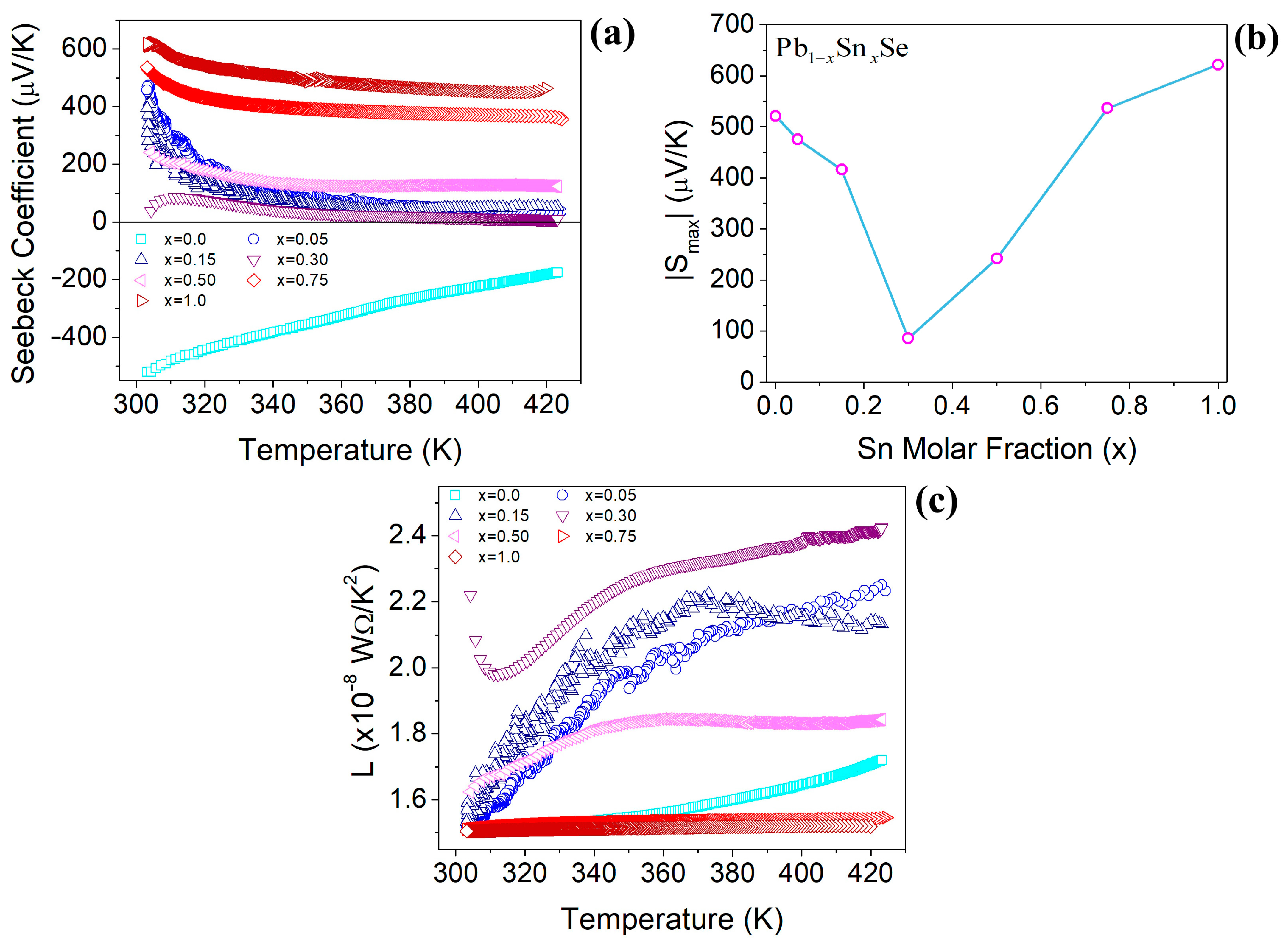
3.4. Seebeck Coefficient Results

Figure 4a shows the measurements of the Seebeck coefficient (S) as a function of the temperature, for the x = 0.0–1.0 alloys. PbSe (x = 0.0) exhibited a Seebeck coefficient that monotonically varied with the temperature, decreasing its magnitude. n-Type conductivity was identified by the negative sign on the S values over the entire temperature range and a maximal value in magnitude of ~520 µV/K. It is well known that native defects in PbSe such as selenium vacancies are responsible for its donor character [2,31], contributing with electrons as majority carriers. These vacancies could be non-intentionally generated by the evaporation of selenium, because of the deposition procedure performed at 300 °C, and x = 0.0 bring the only sample displaying this conductivity type. For the rest of the alloys and x = 1.0, the Seebeck coefficient always resulted in positive values, indicating p-type conductivity. This conductivity ruled by holes also originates from native defects like tin vacancies [32], which additionally compensate for the selenium vacancy concentration produced during the deposition and lead to a residual hole concentration identified by this characterization. As Sn content increased (x = 0.05 and 0.15), the Seebeck coefficient displayed a decrease in its magnitude with the temperature and maximal value (compared with that of x = 0.0), varying sharply over the first 40 K of the temperature range. For Pb0.70Sn0.30Se, the maximal Seebeck coefficient was as low as 87 µV/K, and a slightly different behavior as a function of the temperature was evidenced. Between 300 and 312 K the Seebeck coefficient increased, and above 315 K, it decreased in magnitude with the behavioral as far observed. The very low S value for this alloy is consistent with the shifting towards lower energies of the band gap, similar to what is expected from a conductive material, which exhibits a degenerate carrier concentration. For the same Pb and Sn molar factions, x = 0.50, the Seebeck coefficient magnitude and its maximal value increased relative to the x = 0.30 sample maximal value, and the curve behavior resulted in a soft variation with the temperature. The Seebeck coefficient for x = 0.75 showed similar behavior to the previous case, but large S values in magnitude were displayed; even a greater maximal value (538 µV/K) than that of PbSe or x = 0.05 resulted in this case. Finally, for SnSe (x = 1.0) the Seebeck coefficient varied with the temperature in a similar way to the last cases, where the magnitude and its maximal value resulted in the measured largest values, with a maximum value of ~627 µV/K.
In all cases, for Pb1−xSnxSe x = 0.0–1.0, the Seebeck coefficient behavior always followed a clear trend, which decreased with increasing temperature. This is a classical behavior attributed to a semiconducting material, where electron–hole pairs are thermally excited from the valence band to the conduction band (intrinsic transport regime). Thus, an effective Seebeck coefficient produced a reduction in magnitude due to the opposite sign of the electron and hole Seebeck coefficient contributions, which is in agreement with the following equation [33]:
S = S p σ p + S n σ n σ p + σ n ,
where, S, Sp, Sn, σp, and σn depict the overall, hole, electron Seebeck coefficients, and the hole and electron conductivities, respectively.
The measured Seebeck coefficient maximal magnitude as a function of the nominal composition (x) is displayed in Figure 4b. This behavior of the maximal S magnitude is similar to that observed for the optical band gap energy in Figure 2b. This is completely reasonable since the Seebeck coefficient depends on the energy band structure and therefore on Eg as follows: S ~ E g / 2 k T . Likewise, a similar behavior at room temperature was also observed by Nishimura et al. [21], but with different Seebeck coefficient magnitudes for bulk polycrystalline alloys.
The Seebeck coefficient maximal magnitude provides qualitative information about the majority carrier density since these parameters are inversely related. For x = 0.0 (PbSe), it is possible that a non-degenerate electron density resulted from selenium vacancies because of the obtained large S magnitude of 520 µV/K. As x increased (x = 0.05 and 0.15), tin vacancies were formed in the alloys, likely compensating for the selenium vacancies. Thus, the residual concentration contributed to a low hole density, which increased with the Sn content and displayed a decrease in the maximal S magnitude from 475 µV/K to 410 µV/K. For the x = 0.30 alloy, substitutional Sn heavily doped the PbSe lattice with a large number of vacancies, introducing a shallow acceptor level into the energy band structure and leading to a degenerated hole density (conductor-like) that could be identified by its low Seebeck coefficient magnitude ~87 µV/K and low band gap energy. Furthermore, this value is very close to k / e = 86.173   μ V / K , whose value corresponds to the Sebeck coefficient of a free electron gas. However, by increasing the Sn content again, x ≥ 0.5, the maximal S magnitude increased as well, suggesting a reduction in the hole concentration participating in the transport. Therefore, it is possible that the Sn vacancy concentration is also decreased as a result of the strong bonding of Sn atoms with Se [6], hence reducing the free hole density. For x = 1.0 (SnSe), a non-degenerate hole density is produced by a low tin vacancy concentration, even for stoichiometric conditions [34], giving rise to the largest maximal S magnitude in the order of 627 µV/K. For this case, if Sn-Se has a strong bonding, it is then believed that Se vacancies were not formed during the deposition process.
The influence of additional carriers excited from the gapless surface states (topological insulator behavior for x ≥ 0.30) was not manifested in the thermopower results because, as mentioned by Dziawa and Strauss [4,9], band-inversion depends not only on the composition but also on the temperature. In order to observe the topological insulator behavior, it is necessary to perform Seebeck coefficient measurements at low temperatures.
It is worth mentioning that oxidized species formed during the deposition stage did not affect the electrical transport, since these species promote either p-type conduction with a high charge carrier density or the inversion of the sign of carriers in n-type ultra-thin films at room temperature [35]. Furthermore, it is well known that the oxidation effects can be enhanced at high temperatures, such as the deposition temperature at 300 °C, by bulk oxidation, where both the optical and thermopower properties can be modified, but this did not occur. As our films are very thickly formed by agglomerated nanocrystals, only the exposed surface is oxidized, and this oxidized layer did not significantly impact the hole density nor change the conductivity type in the PbSe film.
On the other hand, the Lorenz number (L) was calculated from the Seebeck coefficient results by the Kim approximation (4) [36] and is shown in Figure 4c for each composition as a function of the temperature.
L = 1.5 + e S 116
where S is the experimental Seebeck coefficient, the above equation is given in 10−8 WΩ/K2 and µV/K units for L and S, respectively. Herein, the Lorenz number was estimated to support the elucidation mentioned above about the majority carrier density.
Around room temperature and for the x = 0.0, 0.05, 0.15, 0.75, and 1.0 alloys, the films have a low carrier density due to the values close to 1.51 × 10⁻⁸ WΩ/K2 corresponding to the non-degenerate limit. For the x = 0.50 alloy, the Lorenz number resulted in 1.63 × 10⁻⁸ WΩ/K2, a value slightly larger, indicating a higher charge carrier density than those of the above alloys, whereas for x = 0.30, it has a high carrier density because the L value resulting in around 2.23 × 10⁻⁸ WΩ/K2, close to the degenerate limit defined by the Wiedemann–Franz law (2.44 × 10⁻⁸ WΩ/K2) for conductive materials. As the temperature increases, the Lorenz number increases as well. This is a consequence of the thermally excited electron–hole pairs, which contribute to raising the overall carrier concentration, but also these charge carriers transport thermal energy, increasing their average energy. The parameters that determine both the charge and the thermal energy transported are the electrical and electronic thermal conductivities, where the Lorenz number depicts the ratio of the thermal to electrical conductivity.
A comparison of our results with non-intentionally doped analog thermoelectric materials, in the same temperature range and displaying similar topological behavior, is presented in Table 1. The 100% lead compounds exhibit high Seebeck coefficients with relatively low and different carrier concentrations, as well as opposite conductivity types. In contrast, the 100% tin compounds show significantly different Seebeck coefficient values and Lorenz numbers, indicating that SnTe is a heavily degenerate semiconductor compared to SnSe, both with p-type conductivities. As for the alloys with similar compositions, for x = 0.30, our sample turned out to be more degenerate, resembling a semimetal, and for x = 0.75, a similar trend is observed as seen between SnSe and SnTe, with p-type conductivity prevailing.

4. Conclusions

Nanostructured Pb1−xSnxSe alloy films, x = 0.0 to 1.0, were successfully synthesized and sprayed as films at 300 °C by using propylene glycol as a dispersant and a component of the deposition solution. For the nominal compositions 0.0 ≤ x ≤ 0.75 assessed in this study, a well-crystalized rock-salt cubic phase as the main phase was obtained related to the alloy formation. Oxidized Pb and Se phases produced during the deposition were identified and appeared mostly from x = 0.05 to x = 0.50. Layered SnSe with a deformed orthorhombic crystal structure that resembled a cubic one, consistent with a 2D to 3D displacive transformation was observed for the 0.30 ≤ x ≤ 0.75 alloys. The deformation of the layered SnSe lattice that occurred in the chemical synthesis allowed Sn incorporation even up to x = 0.75, according to our proposed Vegard law. Hence, this chemical pathway is an alternative to extend the solubility limit. As for x = 1.0, orthorhombic SnSe crystallized as the main phase, with orthorhombic Se and SnSe2 as the secondary phases. Nanostructured crystals for the extremes x = 0.0 and x = 1.0, PbSe and SnSe, respectively, resulted in 16–16.5 nm in size, where all the alloys with nanostructured morphology were formed as well. The Pb1−xSnxSe alloy films showed a shift in their optical structure and absorption edge, revealing a singular behavior of the band gap energy with the composition (x), decreasing for 0.0 ≤ x ≤ 0.30 and increasing for x > 0.30. Such a decrease in band gap energy was consistent with the transition from trivial insulators to topological insulator behavior.
The morphology of the alloyed films was developed by self-assembly processes involved during the synthesis and deposition. Large semispherical- and faceted-shaped crystal formation for x < 0.30, platelets-like 2D-PbSnSe structures mixed with 3D granular crystals of PbSe alloyed with Sn in x = 0.30 and for x = 1.0 were observed as 3D large granular crystals, a different morphology to that observed in x = 0.30 and produced by a long reaction time. Seebeck coefficient measurements assayed in the 300–420 K temperature range of each alloy displayed an intrinsic semiconductor behavior. For x = 0.0 (PbSe), n-type conductivity was exhibited, whereas for the rest of the alloys and x = 1.0 (SnSe) p-type conductivity was observed. In turn, for x ≤ 0.15 and x ≥ 0.50 low carrier concentrations with large Seebeck coefficients and a heavy hole concentration for x = 0.30 with the lowest Seebeck coefficient were obtained. The maximal Seebeck coefficient magnitude as a function of the nominal Sn content behaved similarly to that observed in the band gap energy, manifesting the influence of the carrier concentration, energy band structure, and therefore of Eg.

Supplementary Materials

The following supporting information can be downloaded at: https://www.mdpi.com/article/10.3390/micro5010013/s1, 1. The substrate effect on Seebeck coefficient measurements of the films. References [38,39] are cited in the supplementary materials.

Author Contributions

Conceptualization, E.D.-T. and M.O.-L.; methodology, E.D.-T.; validation, E.D.-T. and Á.G.-C.; formal analysis, E.D.-T.; investigation, E.D.-T.; resources, M.O.-L.; writing—original draft preparation, E.D.-T.; writing—review and editing, E.D.-T., Á.G.-C. and M.O.-L.; visualization, E.D.-T., Á.G.-C. and M.O.-L.; supervision, M.O.-L.; project administration, M.O.-L. All authors have read and agreed to the published version of the manuscript.

Funding

This work was supported by CONAHCYT-México (Grant No. 332038) by a postdoctoral fellowship to E.D.-T.

Institutional Review Board Statement

Not applicable.

Informed Consent Statement

Not applicable.

Data Availability Statement

Data are contained within the article.

Acknowledgments

The authors wish to acknowledge Álvaro Guzmán Campuzano for the valuable technical assistance in the synthesis and processing of the samples, Adolfo Tavira Fuentes for XRD measurements, and Jorge Roque de la Puente from LANE-CINVESTAV-IPN for the electron microscopy images.

Conflicts of Interest

The authors declare no conflicts of interest.

References

  1. Tan, G.; Zhao, L.-D.; Kanatzidis, M.G. Rationally designing high-performance bulk thermoelectric materials. Chem. Rev. 2016, 116, 12123–12149. [Google Scholar] [CrossRef]
  2. Dalven, R. A review of the semiconductor properties of PbTe, PbSe, PbS and PbO. Infrared Phys. 1969, 9, 141–184. [Google Scholar] [CrossRef]
  3. Sun, Y.; Zhong, Z.; Shirakawa, T.; Franchini, C.; Li, D.; Li, Y.; Yunoki, S.; Chen, X.-Q. Rocksalt SnS and SnSe: Native topological crystalline insulators. Phys. Rev. B 2013, 88, 235122. [Google Scholar] [CrossRef]
  4. Dziawa, P.; Kowalski, B.J.; Dybko, K.; Buczko, R.; Szczerbakow, A.; Szot, M.; Łtusakowska, E.; Balasubramanian, T.; Wojek, B.M.; Berntsen, M.H.; et al. Topological crystalline insulator states in Pb1-xSnxSe. Nat. Mater. 2012, 11, 1023–1027. [Google Scholar] [CrossRef]
  5. Guo, C.; Wang, D.; Zhang, X.; Zhao, L.-D. One-One Correspondence between n-Type SnTe Thermoelectric and Topological Phase Transition. Chem. Mater. 2022, 34, 3423–3429. [Google Scholar] [CrossRef]
  6. Wu, C.-F.; Wei, T.-R.; Li, J.-F. Electrical and thermal transport properties of Pb1-xSnxSe solid solution thermoelectric materials. Phys. Chem. Chem. Phys. 2015, 17, 13006–13012. [Google Scholar] [CrossRef]
  7. Woolley, J.C.; Berolo, O. Phase Studies of the Pb1-xSnxSe Alloys. Mater. Res. Bull. 1968, 3, 445–450. [Google Scholar] [CrossRef]
  8. Hoff, G.F.; Dixon, J.R. Electrical Properties of Pb1-xSnxSe Semiconductor Alloys. Solid State Commun. 1972, 10, 433–437. [Google Scholar] [CrossRef]
  9. Strauss, A.J. Inversion of Conduction and Valence Bands in Pb1-xSnxSe Alloys. Phys. Rev. 1967, 157, 608–611. [Google Scholar] [CrossRef]
  10. Reddy, P.D.; Nordin, L.J.; Hughes, L.B.; Preidl, A.-K.; Mukherjee, K. Expanded Stability of Layered SnSe-PbSe Alloys and Evidence of Displacive Phase Transformation from Rocksalt in Heteroepitaxial Thin Films. ACS Nano 2024, 18, 13437–13449. [Google Scholar] [CrossRef]
  11. Neupane, M.; Xu, S.-Y.; Sankar, R.; Gibson, Q.; Wang, Y.J.; Belopolski, I.; Alidoust, N.; Bian, G.; Shibayev, P.P.; Sanchez, D.S.; et al. Topological phase diagram and saddle point singularity in a tunable topological crystalline insulator. Phys. Rev. B 2015, 92, 075131. [Google Scholar] [CrossRef]
  12. Saghir, M.; Sanchez, A.M.; Hindmarsh, S.A.; York, S.J.; Balakrishnan, G. Nanomaterials of the Topological Crystalline Insulators, Pb1-xSnxTe and Pb1-xSnxSe. Cryst. Growth Des. 2015, 15, 5202–5206. [Google Scholar] [CrossRef]
  13. Markov, V.F.; Tretyakova, N.A.; Maskaeva, L.N.; Bakanov, V.M.; Mukhamedzyanov, H.N. Hydrochemical synthesis, structure, semiconductor properties of films of substitutional Pb1-xSnxSe solid solutions. Thin Solid Films 2012, 520, 5227–5231. [Google Scholar] [CrossRef]
  14. Liu, Y.; Lee, S.; Fiedler, C.; Spadaro, M.C.; Chang, C.; Li, M.; Hong, M.; Arbiol, J.; Ibáñez, M. Enhancing thermoelectric performance of solution-processed polycrystalline SnSe with PbSe nanocrystals. Chem. Eng. J. 2024, 490, 151405. [Google Scholar] [CrossRef]
  15. Pei, Y.; Shi, X.; LaLonde, A.; Wang, H.; Chen, L.; Snyder, G.J. Convergence of electronic bands for high performance bulk thermoelectrics. Nature 2011, 473, 66–69. [Google Scholar] [CrossRef] [PubMed]
  16. Wang, C.; Zhang, G.; Fan, S.; Li, Y. Hydrothermal synthesis of PbSe, PbTe semiconductor nanocrystals. J. Phys. Chem. Sol. 2001, 62, 1957–1960. [Google Scholar] [CrossRef]
  17. Tomm, J.W.; Sumpf, B.; Herrmann, K.; Szczerbakow, A. Some aspects of the technology of lead salt diode lasers used in gas monitoring systems. Cryst. Res. Technol. 1987, 22, 981. [Google Scholar] [CrossRef]
  18. Ravich, Y.I.; Efimova, B.A.; Smirnov, I.A. Semiconducting Lead Chalcogenides. In Monographs in Semiconductor Physics, 1st ed.; Stil’bans, L.S., Ed.; Springer: New York, NY, USA, 1970; Volume 5, pp. 15–377. [Google Scholar]
  19. Chen, P.; Wu, Z.; Shi, Y.; Li, C.; Wang, J.; Yang, J.; Dong, X.; Gou, J.; Wang, J.; Jiang, Y. High-performance silicon-based PbSe-CQDs infrared photodetector. J. Mater Sci. Mater. Electron. 2021, 32, 9452–9462. [Google Scholar] [CrossRef]
  20. Feng, W.; Li, Z.; Chen, Y.; Chen, J.; Lang, H.; Wan, J.; Gao, Y.; Dong, H. Enhanced photoelectric properties of PbSnSe thin films via quick oxygen ion-implantation sensitization. J. Mater Sci. 2022, 57, 1881–1889. [Google Scholar] [CrossRef]
  21. Nishimura, Y.; He, X.; Katase, T.; Tadano, T.; Ide, K.; Kitani, S.; Hanzawa, K.; Ueda, S.; Hiramatsu, H.; Kawaji, H.; et al. Electronic and Lattice Thermal Conductivity Switching by 3D-2D Crystal Structure Transition in Nonequilibrium (Pb1−xSnx)Se. Adv. Electron. Mater. 2022, 8, 2200024. [Google Scholar] [CrossRef]
  22. Huang, Z.; Wang, D.; Li, C.; Wang, J.; Wang, G.; Zhao, L.-D. Improving the thermoelectric performance of p-type PbSe. J. Mater. Chem. A 2020, 8, 4931–4937. [Google Scholar] [CrossRef]
  23. Qin, B.; He, W.; Zhao, L.-D. Estimation of the potential performance in p-type SnSe crystals through evaluating weighted mobility and effective mass. J. Materiomics 2020, 6, 671–676. [Google Scholar] [CrossRef]
  24. McCann, P.J. Thermoelectric Materials. US Patent 0055528 A1, 8 March 2012. [Google Scholar]
  25. Webber, D.H.; Buckley, J.J.; Antunez, P.D.; Brutchey, R.L. Facile dissolution of selenium and tellurium in a thiol-amine solvent mixture under ambient conditions. Chem. Sci. 2014, 5, 2498–2502. [Google Scholar] [CrossRef]
  26. Díaz-Torres, E.; Roque, J.; Arreola-Pina, A.S.; Pérez-Guzmán, M.A.; Ortega-Amaya, R.; Ortega-López, M. Nanostructured PbSe Films Deposited by Spray Pyrolysis Using PbSe Colloidal Solutions. Nanomaterials 2023, 13, 2595. [Google Scholar] [CrossRef]
  27. Burkov, A.T. Measurements of Resistivity and Thermopower. In Thermoelectrics Handbook: Micro to Nano, 1st ed.; Rowe, D.M., Ed.; CRC Press Taylor and Francis: Boca Raton, FL, USA, 2006; pp. 22-1–22-12. [Google Scholar]
  28. Patterson, A.L. The Scherrer formula for X-ray particle size determination. Phys. Rev. 1939, 56, 978–982. [Google Scholar] [CrossRef]
  29. Katase, T.; Takahashi, Y.; He, X.; Tadano, T.; Ide, K.; Yoshida, H.; Kawachi, S.; Yamaura, J.; Sasase, M.; Hiramatsu, H.; et al. Reversible 3D-2D structural phase transition and giant electronic modulation in nonequilibrium alloy semiconductor, lead-tin-selenide. Sci. Adv. 2021, 7, eabf2725. [Google Scholar] [CrossRef]
  30. Díaz-Torres, E.; Ortega-López, M.; Matsumoto, Y.; Santoyo-Salazar, J. Simple synthesis of PbSe nanocrystals and their self-assembly into 2D ‘flakes’ and 1D ‘ribbons’ structures. Mater. Res. Bull. 2016, 80, 96–101. [Google Scholar] [CrossRef]
  31. Liu, Y.; You, L.; Wang, C.; Zhang, J.; Yang, J.; Guo, K.; Luo, J.; Zhang, W. Enhancing Thermoelectric Performance of PbSe by Se Vacancies. J. Electron. Mater. 2018, 47, 2584–2590. [Google Scholar] [CrossRef]
  32. Huang, Y.; Wang, C.; Chen, X.; Zhuo, D.; Du, J.; Wang, S.; Ning, L. First-principles study on intrinsic defects of SnSe. RSC Adv. 2017, 7, 27612–27618. [Google Scholar] [CrossRef]
  33. Gibbs, Z.M.; Kim, H.-S.; Wang, H.; Snyder, G.J. Band gap estimation from temperature dependent Seebeck measurement–Deviations from the 2e|S|maxTmax relation. Appl. Phys. Lett. 2015, 106, 022112. [Google Scholar] [CrossRef]
  34. Chen, C.-L.; Wang, H.; Chen, Y.-Y.; Day, T.; Snyder, G.J. Thermoelectric properties of p-type polycrystalline SnSe doped with Ag. J. Mater. Chem. A 2014, 2, 11171–11176. [Google Scholar] [CrossRef]
  35. Rogacheva, E.I.; Tavrina, T.V.; Grigorov, S.N.; Nashchekina, O.N.; Volobuev, V.V.; Fedorov, A.G.; Nasedkin, K.A.; Dresselhaus, M.S. Effect of Oxidation on the Thermoelectric Properties of PbSe Thin Films. J. Electron. Mater. 2002, 31, 298–303. [Google Scholar] [CrossRef]
  36. Kim, H.-S.; Gibbs, Z.M.; Tang, Y.; Wang, H.; Snyder, G.J. Characterization of Lorenz number with Seebeck coefficient measurement. APL Mater. 2015, 3, 041506. [Google Scholar] [CrossRef]
  37. Chen, Y.-X.; Li, F.; Li, D.; Zheng, Z.; Luo, J.; Fan, P. Thermoelectric Properties of Tin Telluride Quasi Crystal Grown by Vertical Bridgman Method. Materials 2019, 12, 3001. [Google Scholar] [CrossRef] [PubMed]
  38. Díaz-Torres, E.; Flores-Conde, A.; García-Ávila, A.; Ortega-López, M. Electronic transport study of PbSe pellets prepared from self-assembled 2D-PbSe nanostructures. Curr. Appl. Phys. 2018, 18, 226–230. [Google Scholar] [CrossRef]
  39. Matsuura, H.; Riss, A.; Garmroudi, F.; Parzer, M.; Bauer, E. Cooperative Nernst effect of multilayer systems: Parallel circuit model study. Phys. Rev. Res. 2024, 6, 043071. [Google Scholar] [CrossRef]
Figure 1. XRD patterns of the sprayed films (a) PbSe (x = 0.0), the x = 0.05–0.75 alloys, and SnSe (x = 1.0). (b) Lattice constant as a function of the nominal Sn molar fraction (x) obtained by analyzing the (311) and (222) peaks of each alloy, the solid line is the fit curve corresponding to Equation (1). Cross, star, circle, and caret marks indicate oxidized phases in the films, whereas ampersand and number sign marks indicate secondary phases in x = 1.0. Vertical continuous lines are used to identify the PbSe reference, ICDD 00-006-0354, dashed lines correspond to the cubic SnSe pattern, ICDD 01-089-4781, and dotted lines were attributed to orthorhombic SnSe, according to ICDD 00-048-1224 pattern.
Micro 05 00013 g001
Figure 2. (a) Absorption spectra vs. the photon energy and (b) optical band gap energy vs. the nominal composition at room temperature for the sprayed Pb1−xSnxSe x = 0.0–1.0 alloy films. Inset, optical band gap energy vs. the Sn content for the x = 0.0–0.30 alloys and data linear fit.
Micro 05 00013 g002
Figure 3. Representative SEM images of (a) PbSe (x = 0.0), (b) x = 0.30 alloy, and (c) SnSe (x = 1.0). Inset in (b) shows the platelets of the segregated 2D-PbSnSe phase.
Micro 05 00013 g003
Figure 4. (a) Seebeck coefficient as a function of the temperature, (b) Seebeck coefficient maximal magnitude as a function of the nominal composition (x) between room temperature and 313 K, and (c) Lorenz number vs. the temperature for the sprayed Pb1−xSnxSe x = 0.0–1.0 alloy films. Positive Seebeck values indicate p-type conductivity and negative ones indicate n-type conductivity.
Micro 05 00013 g004
Table 1. Comparison of Seebeck coefficient and calculated Lorenz number values for analog materials (Te-based) to those of the alloys reported in this work (Se-based), in the 300–423 K temperature range.
MaterialS (µV/K)L (WΩ/K2)
PbTe310–360 [5]1.57–1.55 × 10⁻⁸ [5]
Pb0.70Sn0.30Te70–150 [5]2.05–1.77 × 10⁻⁸ [5]
Pb0.30Sn0.70Te50–80 [5]2.15–2.00 × 10⁻⁸ [5]
SnTe35–39 [37]2.29–2.22 × 10⁻⁸ [37]
PbSe−520–(−175)1.51–1.72 × 10⁻⁸
Pb0.70Sn0.30Se87–101.97–2.42 × 10⁻⁸
Pb0.25Sn0.75Te538–3571.51–1.55 × 10⁻⁸
SnSe627–449~1.51 × 10⁻⁸
Disclaimer/Publisher’s Note: The statements, opinions and data contained in all publications are solely those of the individual author(s) and contributor(s) and not of MDPI and/or the editor(s). MDPI and/or the editor(s) disclaim responsibility for any injury to people or property resulting from any ideas, methods, instructions or products referred to in the content.

