Article

Hybrid CuI@g-C3N4/MoS2 Thin Films for Energy Conversion Applications: A Photoelectrochemical Characterization

by
Daniel Arturo Acuña Leal
1,*,
Claudia Rosa Santiago Ramírez
1,
Norma A. Ramos Delgado
2,
Sadasivan Shaji
3,
Bindu Krishnan
3,
David Avellaneda Avellaneda
3,
Josue Amilcar Aguilar Martínez
4,
Shadai Lugo Loredo
5,
Arian Espinosa Roa
6 and
Miguel Ángel Gracia Pinilla
1,*
1
Facultad de Ciencias Físico Matemáticas, Universidad Autónoma de Nuevo León, Av. Pedro de Alba S/N, San Nicolás de los Garza 66455, Nuevo León, Mexico
2
Instituto Tecnológico de Nuevo León, Centro de Investigación e Innovación Tecnológica, Av. De la Alianza No. 507 Parque PIIT, Km. 10 Autopista al Aeropuerto Internacional Mariano Escobedo, Apodaca 66629, Nuevo León, Mexico
3
Facultad de Ingeniería Mecánica y Eléctrica, Universidad Autónoma de Nuevo León, Av. Pedro de Alba S/N, San Nicolás de los Garza 66455, Nuevo León, Mexico
4
Centro de Investigación en Innovación en Ingeniería Aeronáutica, Universidad Autónoma de Nuevo León, Carretera a Salinas Victoria Km. 24.5, Apodaca 66600, Nuevo León, Mexico
5
Facultad de Ciencias Químicas, Universidad Autónoma de Nuevo León, Av. Pedo de Alba S/N, San Nicolás de los Garza 66455, Nuevo León, Mexico
6
CONAHCyT-Centro de Investigación en Química Aplicada (CIQA), Unidad Monterrey, Alianza Sur no. 204, Parque de Investigación e Innovación Tecnológica (PIIT), km 10 Autopista Internacional Mariano Escobedo, Apodaca 66628, Nuevo León, Mexico
*
Authors to whom correspondence should be addressed.
Photochem 2025, 5(1), 9; https://doi.org/10.3390/photochem5010009
Submission received: 30 December 2024 / Revised: 27 February 2025 / Accepted: 7 March 2025 / Published: 18 March 2025

Abstract

:
In this work, we report the fabrication of CuI@g-C3N4/MoS2 thin films by the thermal evaporation of Cu films and their conversion into hybrid films by a simple wet chemical method. Compared to pure CuI, CuI@g-C3N4/MoS2 shows enhanced absorption near the UV region, which improves its DC photoconductivity. The conductivity of the films is enhanced by the addition of g-C3N4/MoS2, which is distributed on the surface of the CuI film. The band gap of the films red-shifts upon adding g-C3N4/MoS2. We evaluate this material’s potential application as a photodetector and in photocatalysis by evaluating its photoelectrochemical properties using impedance spectroscopy measurements, cyclic voltammetry, and DC photoresponse measurements. We find that upon the addition of g-C3N4/MoS2, the conductivity of the films is increased, as evidenced by the time-dependent photo amperometry measurements. Also, a higher DC photoresponse is observed upon increasing the concentration of MoS2. This work marks the first time a hybrid CuI@g-C3N4/MoS2 film and its photoelectrochemical characteristics have ever been reported.

Graphical Abstract

1. Introduction

Transparent semiconductor thin films are promising due to their applications in transparent electronics, such as OLED and AMOLED displays. Projections are such that this kind of technology is predicted to dominate an important portion of the near-future market [1]. Usually, semiconducting oxide thin films possess n-type conductivity, and their wide band gaps lead to efficient electron injectionn due to their bonding properties, so, from a technological point of view, it is important to produce p-type transparent semiconductors. The first instance of a p-type transparent semiconductor was proposed by Kawazoe et al., who reported a Delafossite CuAlO2 [2]. Since then, many researchers have explored different materials, such as NiO [3] and Cu-Cr-O Delafossites [4], perovskites such as SrCuO3, oxichalcogenides, and CuxO [5,6]. Among the available p-type transparent semiconductors, CuI is an important material with a direct band gap of 3.1 eV, relatively high hole mobility of 44 cm2/V-s, high p-type conductivity, and high carrier concentrations of up to 1020 cm−3 [7]. The conductivity of the films can be modified by tuning the charge carrier concentrations by doping [8]. The material can be easily synthesized by many methods, such as thermal evaporation [9] and sputtering. Many devices based on transparent p-type CuI have been reported in the literature. One example is a transparent self-powered photodiode based on γ-CuI/β-Ga2O3 deposited using the thermal evaporation of the starting salts. This work reported a high rectification ratio and UV photovoltaic action [10]. Kim and co-workers obtained an n-ZnO/p-CuI with a passivation film made of ZnS. In their work, the rectification ratio of the n-ZnO/p-CuI was improved to 107 by employing a ZnS film in between the ZnO and the CuI; this helped to passivate the oxygen vacancies, which improved the rectification ratio [11]. Some other materials employed for transparent diodes based on CuI are BaSnO3 [12], SiZnSnO [13], AgI [14], and NiI2 [15]. These materials provide a high rectification ratio and, thus, high-quality junction and electrical properties of the diode; however, their application is limited by the complicated nature and high cost of the experimental techniques used to obtain the materials and their desired properties. A way to tune and optimize material properties is by blending materials with other organic or inorganic materials to form hybrid films. Among the materials used to make hybrid films, the n-type material g-C3N4 is a relatively new and unexplored option for optoelectronic applications coupled with CuI. Usually, carbon nitride thin films find extensive applications in photocatalysis [16], anticorrosion coatings [17], perovskite solar cells [18], and solar fuel generation [19,20,21], among others. One example is carbon nitride thin films with a graphene-like structure in which an infinite extension of triazine rings or tri-s-triazine rings forms the basic structural unit. This kind of structure allows a unique electronic structure and crystal sites that allow the material to have a large surface area and, hence, more active sites for charge separations. The covalent bonding from the structural unit allows the material to have excellent chemical and thermal stability up to 600 °C. Its conduction and valence band positions and moderate bang gap of 2.7 eV make it an attractive material for photodiodes and solar cells [22]. The material has some drawbacks, such as its high recombination rate, low conductivity, and low specific surface area, which are easily improved by various methods, most of which are compatible with low-cost solution methods [23]. Depending on the application, the properties of carbon nitride can be tuned by controlling the defects on the material, or by passivation effects from the carbon nitride itself, acting as an additive [24]. For example, the band gap of g-C3N4 can be tuned with MoS2 to form a hybrid material with an extended absorption edge near the visible spectrum so the material can utilize more photons of the visible spectrum and tune the optoelectronic properties of the material [25]. MoS2 possesses an indirect band gap of 1.8 eV, which changes to a direct one when it is in the form of thin sheets. This material has a 2H hexagonal crystalline structure, which makes it compatible with carbon nitride. Its optical and electrical properties allow it to be used in different applications, such as sensors, photodetectors, photocatalysis, etc. [26]. Quantum dots of MoS2 were embedded in g-C3N4 by mixing both powders appropriately. The resulting hybrid materials modified the absorption edge of the carbon nitride from 2.62 eV to 2.52 eV [27]. The simple mechanical milling of the exfoliated powders of both MoS2 and C3N4 leads to a hybrid material with an absorption edge red-shifted to 500 nm, compared to the fundamental edge of carbon nitride near 400 nm [28]. Films of g-C3N4/GO/MoS2 were prepared using a simple hydrothermal method. Incorporating the hybrid nanocomposite improved the photocurrent of the material by four times compared to the pristine carbon nitride material [29]. A heterojunction thin film of MoS2/g-C3N4 was employed to increase the photocurrent of pristine carbon nitride. Aside from the shift to 1.69 eV, there was an improvement in the charge transfer due to the heterojunction [30]. Control of charge transfer is important for electronic applications, as it influences the rectification ratio and, thus, the quality of the diode. An appropriate band positioning of the respective n- and p-type semiconductor materials can modify charge transfer. The modification of band positioning can be achieved by the hybridization of the materials and doping. Carbon nitride offers a simple way of controlling band positions using chemical engineering and non-chemical methods [31]. Theoretical studies show that nanosheets of g-C3N4 can enhance the material’s conductivity [32]. So far, the only works reported on the heterojunction of CuI with g-C3N4 are for photocatalysis, supercapacitors, and hydrogen production [33,34,35]. Based on the lack of studies on CuI modified with MoS2/g-C3N4, we report for the first time a hybrid film based on CuI with a surface modification of particles of g-C3N4/MoS2. We establish this composite’s optical and electrical properties by employing DC photoresponse and impedance spectroscopy. We find an increase in conductivity and charge transfer upon adding g-C3N4/MoS2 into the CuI film.

2. Materials and Methods

2.1. Synthesis of CuI@g-C3N4/MoS2 Thin Films

2.1.1. Chemicals

This study used Cu beads (Cu, 99.99% purity), iodine powder (Fermont, 99.999% purity), melamine (Sigma, St. Louis, MO, USA, 99%), glycine (Sigma, purity > 98%), and 2-propanol. The reagents were used as received without further purification.

2.1.2. Synthesis of CuI Thin Films

FTO-coated glass (Qunguan 7–8 Ω/m2) and soda–lime glass (Corning) were cut to form a glass 25 × 25 × 1.2 mm in size in the case of FTO and 25 × 25 × 0.7 m in size in the case of soda–lime glass. Subsequently, these substrates were cleaned in an ultrasonic bath, employing a soap solution, water, and ethanol for 10 min each. Afterward, the substrates were cleaned with dry air. The cleaned substrates were placed in a thermal evaporation system (Torr International (Marlboro, NY, USA), Model No: THE2-2.5 kW-TP) at a constant rate of 2 Å/s under a high vacuum of 10-6 Torr. The thickness of the Cu layer was kept at 50 nm, as measured with a quartz detector and profilometry. The as-grown Cu layers were removed from the system and dipped in an I2 solution at a fixed concentration of 0.15 M for 1 min. The films were readily converted into CuI, as evidenced by the color change from metallic and shiny brown to transparent reflective film. Afterward, they were washed with pure 2-propanol and dried with a gentle airflow.

2.1.3. Synthesis of g-C3N4/MoS2 Composite

To synthesize the composite, we followed the subsequent methodology: First, we synthesized g-C3N4 via thermal decomposition of melamine on a conventional muffle furnace at 550 °C for 4 h, using a ramp of 2 °C/min. The as-prepared powder was pulverized to homogenize the particle size. Next, we prepared a colloidal suspension of the powders in 2-propanol at a concentration of 3 mg/mL and sonicated it for 24 h to obtain the graphitic form of the carbon nitride. To obtain the g-C3N4/MoS2 composite, we added 1%, 3%, and 5% powder of MoS2 to the previously mentioned colloidal suspension. The sonication process was repeated for these colloidal suspensions to obtain the composites.

2.1.4. Synthesis of CuI@g-C3N4/MoS2 Hybrid Thin Films

The composite CuI@g-C3N4/MoS2 was obtained using the previously prepared colloidal suspension to dissolve the iodine powder at a concentration of 0.15 M. The Cu films were dipped in these solutions (concentration of g-C3N4 3mg/mL; concentration of MoS2 varied based with respect to the concentration of g-C3N3 as, 1%, 3%, and 5% of weight) for 1 min, rinsed with 2-propanol, and dried with a gentle flow of warm air. These samples were labeled as CNM-1, 2, and 3, respectively.

2.2. Characterization

Structural characterization was conducted using a PANalytical (Malvern, UK) diffractometer in the 2θ range of 10–70° using a step size of 0.01° with a time per step of 10 s. Vibrational spectra were obtained with a DXR 2 Raman Microscope (Thermo, Waltham, MA, USA) with a 532 nm wavelength laser. The optical absorption, specular transmission, and reflection of the films were measured with a Uv-Vis-NIR Jasco V-770 Spectrophotometer (Thermo). The morphology of the films was studied with a Scanning Electron Microscope (SEM), Hitachi SU 8020 (Tokyo, Japan). A Transmission Electron Microscope JEOL 2010 (USA, MA)was employed to observe the interfacial characteristics of the composites. The chemical composition of the samples was determined by an X-ray photoelectron Spectrometer (XPS), Thermo K-Alpha, using monochromatized Al-Kα radiation (hv = 1486.68 eV). DC photocurrent measurements were performed with a pico ammeter/voltage source, Keithley 6487 (Cleveland, OH, USA). For this purpose, silver electrodes 5 × 5 mm in size were painted on the surface of the samples deposited in bare glass using Ag colloidal paste (SPI Supplies, Nieuw-Vennep, the Netherlands). The samples were illuminated with a blue LED with 30 W power (power density of 4.8 W/cm2) and a wavelength of 460–465 nm. Electrochemical studies were conducted using an electrochemical workstation (CS350 EIS potentiostat/galvanostat, Corrtest Instruments, Wuhan, China). Cyclic voltammetry (CV), impedance spectroscopy (EIS), and Chronoamperometry (CA) analyses were performed with the CNM-1, CNM-2, and CNM-3 electrodes as photoanodes. Six films were synthesized using the specific method described in Section 2.1, ‘Synthesis of CuI@g-C3N4/MoS2 Thin Films’. Each film was deposited onto an FTO substrate, ensuring an exposed material area of precisely 1 cm2. The synthesized films included CuI, CNM-1, CNM-2, CNM-3, and the reference films CuI@g-C3N4 and CuI@MoS2. Platinum foil was used as a counter electrode and Saturated Calomel Electrode (SCE) as a reference electrode. As the electrolyte, 0.5 M potassium chloride (KCl) solution was chosen. CV profiles were registered from −0.6 V to 0.6 V vs. SCE at scan rates of 100 mVs−1. EIS was performed in open circuit potential (OCP) conditions with a frequency range of 1–105 Hz and an amplitude of 10 mV. Before electrochemical studies were conducted, the solution was kept under an argon atmosphere for 30 min.

3. Results

3.1. Structural Characterization

Figure 1 shows the X-ray diffraction pattern of the CNM-1, CNM-2, and CNM-3 samples. A sample of a pure CuI film was also analyzed for comparison. It is observed that diffraction peaks occur at the 2θ angles of 25.57°, 29.51°, 42.306°, 49.89°, and 52.306°, which are due to the reflections of the (111), (200), (220), (311), and (222) planes of the zinc-blende structure of CuI (pdf number 060246) 29. From the diffraction pattern, the pure CuI film is observed to have a preferential orientation to the (111) family of planes. When the g-C3N4/MoS2 composite is added into the CuI thin films, additional diffraction peaks are observed at 2θ values of 14.53° and 27.48°, which are due to the reflections of the (002) plane of the 2H hexagonal crystal of MoS2 (pdf number 0771716) [36] and (002) plane of the tri-s-triazine building block of g-C3N4 [37]. These peaks are marked with a # and a *, respectively, in the diffractogram. They can be explained by the successful incorporation of the g-C3N4/MoS2 composite into the CuI thin films. The intensity of the MoS2 peak increases as the quantity of the powder increases from 1% wt to 5% wt, which is in agreement with the experiment. The concentration of g-C3N4 is kept constant in all experiments, so the peak intensity is always the same. Since the carbon nitride is in the monolayer form, the respective reflection is expected to have a low peak intensity due to the fewer planes contributing to this peak intensity. No other impurity phases, such as metallic Cu or CuO, are observed.
The average crystallite size of the samples was calculated using Scherrer’s equation [38]:
D = 0.9 λ β c o s θ
where D is the average crystallite size, λ is the diffractometer wavelength, β is the full-width at half maxima of the peak in radians, and θ is the Bragg’s angle in radians.
To conduct the analysis, we selected the (111) reflection of all the samples under consideration. The results showed that the as-prepared sample of CuI thin films shows an average crystallite size of 58 nm. The crystallite size increases slightly in the range from 60 to 65 nm for samples CNM-1, CNM-2, and CNM-3, respectively.
Figure 2 depicts the Raman spectra of all the samples. We observe Raman peaks for all the samples at 121.91 cm1 due to the transverse optical vibrational mode of the Cu-I bond. Peaks appear at 383 and 407 cm1 in sample CNM-3, which are due to the vibrational modes of MoS2, the E2g1 longitudinal in-plane vibration of the S atom plane with adjacent Mo atoms, and the optical mode A1g due to the out-of-plane S vibrations that occur because of optical excitation [39]. The bulk sample of MoS2 is shown in Figure 3. It can be observed that both Raman modes are also present at 378 and 404 cm1, respectively. We observe a red-shift in the A1g mode of the CNM-3 sample. The shift is 4 cm1, which could be due to decreased interlayer interaction [40]. A red-shift in E2g1 is also observed in this sample. This can be explained by the electrical interaction nature of the S-Mo-S layers, since exfoliation plays no significant role in the elastic constant of the S-S vibrational mode. Exfoliation usually tends to decrease the layers of bulk MoS2 to the order of a few layers or even monolayer thickness. Since we observe a red-shift in the mode, we can assume that ionic chalcogen–metal interaction results from this red-shift with decreased layers [41]. Peak intensity also increases when the sample is in the thin film rather than in the bulk phase. This effect is due to the optical interference of the laser radiation and the emitted Raman scattering radiation [41]. The higher background and noise present in this sample could be due to the inelastic scattering produced by the powder sample. All these results confirm that the phases present are crystalline and consist of CuI and the composite material.
The complete conversion of metallic Cu thin films into CuI follows the reaction
2Cu + I2 → 2CuI
in which the iodine from the solution readily reacts with the Cu atoms on the surface of thin films to form solid CuI. The electronegativity value of Cu is listed as 1.9 on the Pauling Scale, and the I electronegativity value is listed as 2.26 on the same scale; this difference explains why the reaction proceeds in 1 min [42]. Other sources of Cu have different reaction kinetics, such as Cu3N, in which the reaction rate is slower than the metallic Cu precursor, due to the differences in electronegativity values [43]. Oxides, such as CuO, can be found after the application of specific deposition methods. For example, Li and co-workers reported that the synthesis of CuI from metallic Cu using a hydrothermal method at 200 °C with a stainless steel autoclave produced CuO on the resulting films [38]. In our case, no oxides can be detected by XRD or Raman. Also, no metallic Cu can be observed from these measurements, so we can conclude that a complete conversion occurred. An increase in thickness from 50 nm to 150 nm is observed in the samples, independent of the concentration of MoS2 employed. This resulting increase in thickness is due to the volume expansion of the lattice upon the addition of iodine. The preferential orientation in the (111) direction is due to the lower surface energy of the respective plane [44].

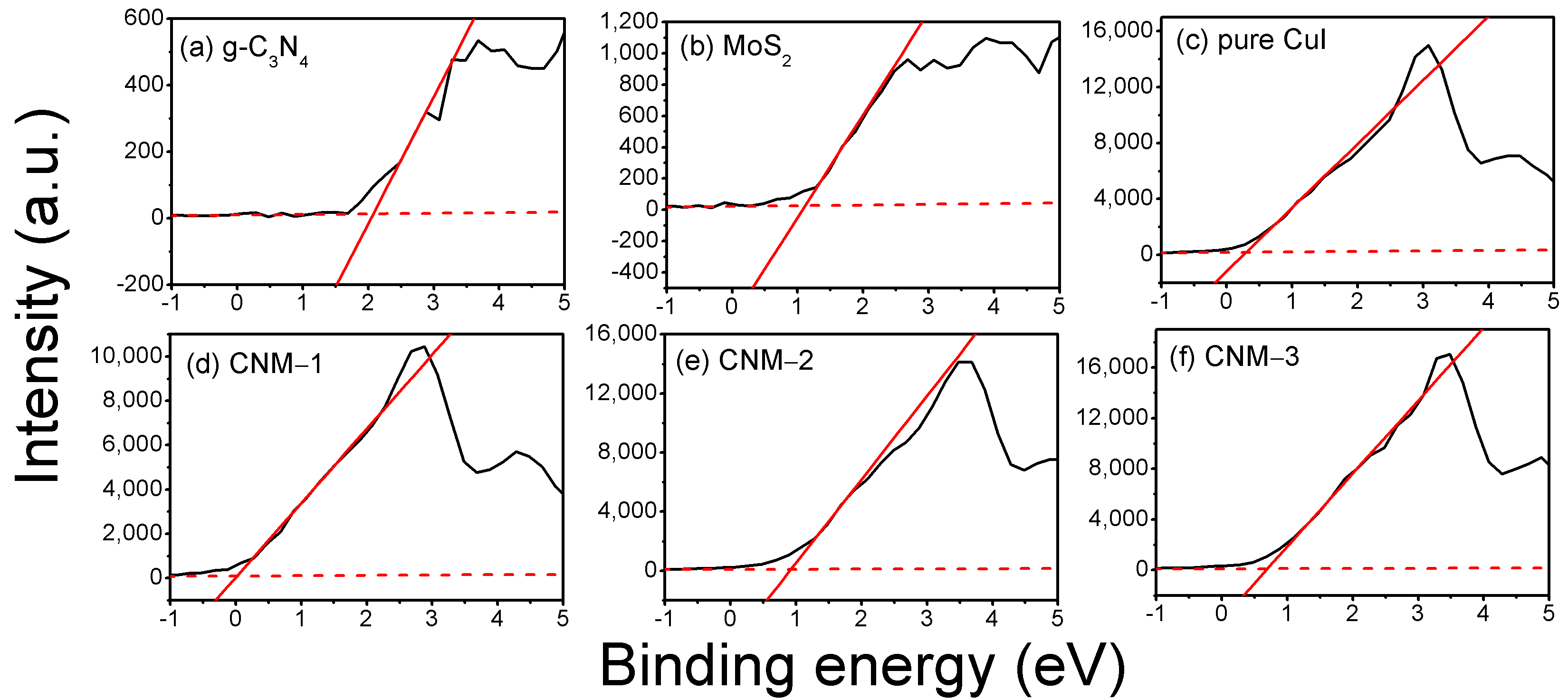
3.2. Chemical Composition
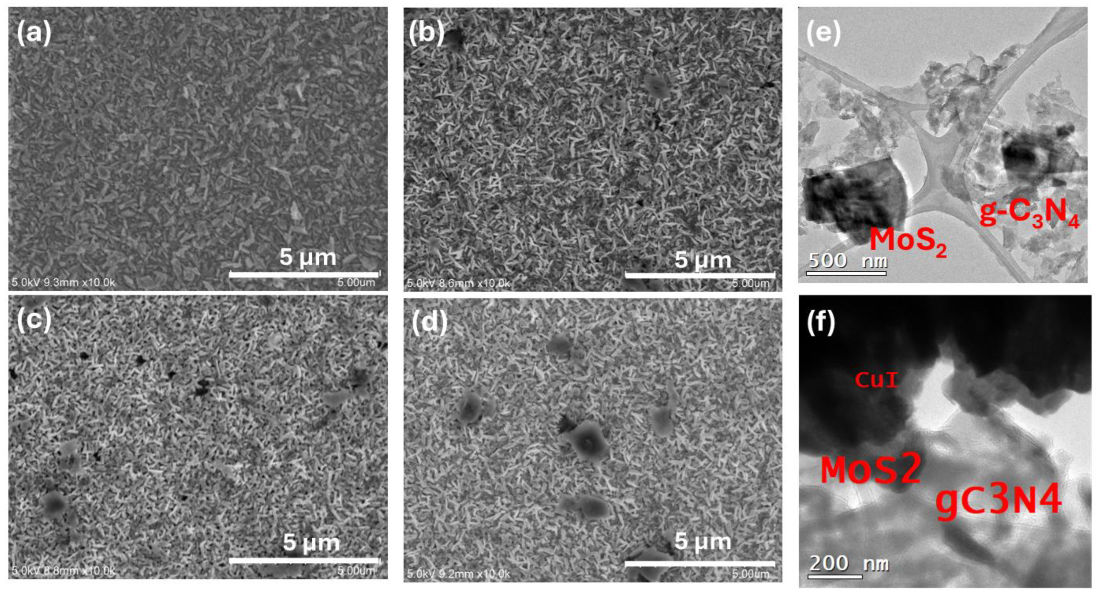
Figure 4 shows the survey spectra and high-resolution spectra of the MoS2 and g-C3N4 powders. Figure 4a shows that only elements corresponding to the starting materials are present in the samples. The small oxygen signals present in the samples might be due to adventitious carbon. No other impurities are observed. Figure 4b shows the high-resolution spectra of the C 1s and N 1s levels for carbon nitride and Mo 3d and S 2p for MoS2 powders. The carbon nitride sample from the melamine precursor shows two distinctive photoelectron peaks for the C 1s core level. The peak at 284.8 eV is due to C=C coordinated carbon, while the peak at 287.98 eV corresponds to the carbon bonded with sp3 hybridization in the C-N=C backbone. For the N 1s core level, the peak at 398.48 eV corresponds to the sp2-bond in N in the triazine rings, and the peak at 399.78 eV is due to three carbons coordinated with a N, labeled as N-(C)3 in the figure. The peak at 400.88 eV is due to the amino functional group present in the carbon nitride [45]. In the case of MoS2, the Mo 3d core level shows a doublet peak, which is centered at 229.68 and 232.78 eV, and these peaks are due to the Mo4+ 3d5/2 and Mo4+ 3d3/2 components present in the MoS2 with 2H symmetry. Also, a small peak is observed for this core level centered at 226.98 eV, which is due to the 2s component of the material. For the S 2p core level, a doublet photoelectron peak is centered at 162.48 eV and 163.68 eV due to the S 2p3/2 and S 2p1/2 components of MoS2. These values agree with the reported values for bulk MoS2 [46]. The Mo 3d level has a spin–orbit coupling component of 3.1 eV and an intensity ratio of 3:2 for Mo 3d5/2 and Mo 3d3/2, respectively. The S 2p level has a spin–orbit coupling component of 1.2 eV and an intensity ratio of 2:1 for the S 2p3/2 and S 2p1/2 components, respectively. These values agree with the reported values found in the literature [47]. The atomic percentage for g-C3N4 is 49.78% for C and 48.89% for N, an almost stoichiometric ratio. The atomic percentage for MoS2 is 13.59% for Mo and 29.12% for S. The atomic ratio for MoS2 is 2.1:1, which is in good agreement with the chemical formula of this compound.
Figure 5 shows the survey spectra for samples CNM-1, CNM-2, and CNM-3. The spectra indicate the presence of Cu, I, C, N, Mo, and S due to the CuI thin films and the composite g-C3N4/MoS2. All the samples present an O 1s signal, which could be due to contamination from adventitious carbon and oxygen.
To gain further insight into the chemical states and chemical interactions of CuI and the composite, we analyze the high-resolution spectra for the core levels C 1s, N 1s, Mo 3d, S 2p, Cu 2p, and I 3d for samples CNM-1, CNM-2, and CNM-3, respectively. The results are presented in Figure 6. It can be observed that for the C 1s core level, there are three different photoelectron peaks centered at 284.6 eV, 286.28 eV, and 288.28 eV, which are due to C-C from graphitic and adventitious carbon on the surface, C-O from adventitious carbon, and the C-N=C backbone, respectively. For the N 1s core level, photoelectron peaks centered at 399.2 eV, 400.6 eV, and 402.3 eV are due to sp2-bonded N in triazine rings, the N-(C)3 coordinated N and the amino functional groups, respectively [45]. An additional signal centered at 395.2 eV is present because of the Mo 3p component due to the Mo-S bond [46]. The Mo 3d core level shows a doublet peak, with the peaks centered at 229.4 eV and 232.5 eV, which are the Mo 3d5/2 and Mo 3d3/2 components of the Mo-S bond, having a spin–orbit component of 3.1 eV. Also, a small peak centered at 226.8 eV is present due to the S 2s photoelectron peak from the Mo-S bond [46]. The S 2p core level has a doublet photoelectron peak, with binding energies of 162.1 and 163.e eV due to the S 2p3/2 and 2p1/2 doublets for the Mo-S bond. They have a spin–orbit coupling component of 1.16 eV [46]. The Cu 2p core level has a doublet peak with binding energies of 932.4 eV and 952.2 eV due to the Cu 2p3/2 and Cu 2p1/2 components of the Cu-I bond. A minor feature at 931.1 eV is due to the iodine photoelectron peak. The I 3d core level has a doublet photoelectron peak with binding energies at 619.8 and 631.3 eV due to the I 3d5/2 and I 3d3/2 components of the Cu-I bond [48]. These results indicate that the Cu film is readily converted into CuI upon reacting with the composite solution of iodine, which confirms our XRD studies. Compared with Figure 4, the intensity of the C-C photoelectron peak greatly intensifies on the thin film. The N-C=N signal is shifted to higher binding energies than the bulk sample. Also, the peak intensity for the C=C peak is stronger than the bulk phase. This shows that adventitious carbon is highly present in thin films. Compared with the bulk phase, in which a higher number of s-triazine units are present, the exfoliated phase can contain fewer units in the bulk, which explains the lower intensity of the N-C=N signal. The signals of the N 1s components are all in the same ratios compared to the bulk sample, which is consistent with previous reports [49]. No changes in the binding energies for the C and N levels are expected upon exfoliation, as previously reported by Gowri and co-workers [50].
The valence band spectra of the samples were analyzed. Figure 7 presents the valence band spectra of the bulk samples and samples CNM-1, CNM-2, and CNM-3, respectively. The valence band edge was extracted from the XPS valence spectrum using a method similar to that in [51]; a straight line is extrapolated from the valence band edge to the onset of the band. The intersection of these two straight lines is the valence band edge. The calculated band edges for the pure samples are 2.06 eV, 1.07 eV, and 0.33 eV for carbon nitride, MoS2, and pure CuI, respectively. For the CuI@g-C3N4/MoS2 thin films, the extrapolated valence band edges are 0.02 eV, 0.97 eV, and 0.7 eV for samples CNM-1, CNM-2, and CNM-3. The valence band for the CNM-1 sample is lowered compared to pure CuI, while the samples CNM-2 and CNM-3 are moved to higher energy levels compared to CuI. This shift in energy comes from the interaction of the electron cloud with π bonding in carbon nitride and from the higher interaction of I species with MoS2 and carbon nitride.

3.3. Morphology

Figure 8 shows the sample’s SEM and high-angle annular dark-field TEM images. Figure 8a shows the SEM micrograph of a pure CuI thin film. The surface morphology of CuI consists of a rough surface with large crystals. Usually, the surface morphology of CuI consists of large and irregularly shaped crystals due to the fast kinetics of the reaction of Cu with the iodine solution. For example, different kinds of morphologies are obtained by the spin coating of CuI powders in acetonitrile solvent, in which conditions such as concentration and doping atoms alter the surface roughness of the film [52]. Figure 8b, Figure 8c, and Figure 8d are the SEM micrographs of samples CNM-1, CNM-2, and CNM-3, respectively. It can be observed that some islands are present on the surface of the film, which are the composite material g-C3N4/MoS2. The film morphology of CNM samples consists of smaller grains than the pure CuI thin film. This is because of a stabilization effect due to the solution of I2, which coordinates with the suspended g-C3N4 to generate a stable suspension [53]. This stable suspension yields higher surface energy to the Cu thin film, which, in return, leads to more uniform film morphology. Different methodologies produce different crystal orientations and morphologies [54]. As some theoretical research has proven, the observation of the agglomerates of g-C3N4/MoS2 leads to a more uneven film surface but can lead to more active sites for photocatalytic reactions [55]. TEM analysis is used to study the g-C3N4/MoS2 agglomerates. Figure 8e is the transmission image of the sample. It can be observed that the largest particle consists of the MoS2 nanoparticles supported on g-C3N4. The carbon nitride consists of only a few layers, as expected from the mechanical exfoliation process. To address the bulk CuI@g-C3N4/MoS2 heterojunction, we performed a dipping process on the Cu grid used to support the composite, resulting in the material being formed on the grid and, simultaneously, supported by it. The high-angle annular dark-field image in Figure 8f confirms this. The thickest material is the formed CuI, while the layered semiconductor is g-C3N4. The corresponding HRTEM micrograph of the interface of MoS2 and g-C3N4 and SAED analysis of the CuI@g-C3N4/MoS2 of sample CNM-3 are shown in Figure S1.

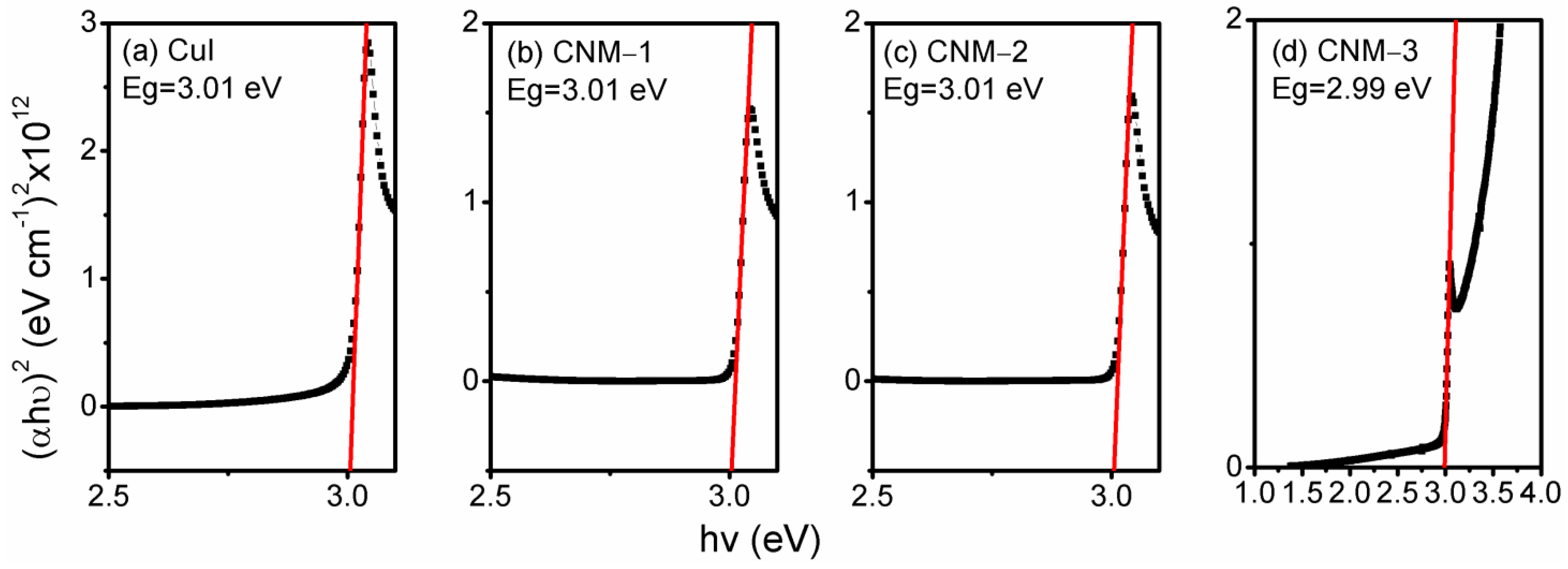
3.4. Optical Properties

Figure 9 shows the absorbance spectra of all the films. It can be observed that all the films possess a strong absorption onset at 400 nm, which corresponds to the fundamental absorption edge. Another strong absorption peak appears at 337 nm, which is due to the transition from the split-off band [56]. The fundamental edge of CuI is of a direct semiconductor, as already reported in the literature [36]. The absorption intensity increases with the increase in the concentration of MoS2, as can be seen in the figure. This increase is due to the absorption of the composite g-C3N4/MoS2 [57]. Absorption decreases upon increasing the concentration from 3% to 5%. This is explained by the SEM micrographs, in which larger particles are observed on the surface of the samples, and thus, this enhances the scattering of light. Absorption onsets from g-C3N4/MoS2 nanomaterials are difficult to observe in the figure. To confirm the presence of these absorption onsets, we calculate the first derivative of the absorption with respect to the wavelength to determine the transitions present in our samples. This method was reviewed by Ojeda and Rojas [58] and implemented by Trenczek-Zajac and co-workers [59]. The derivate equals zero at the wavelength at which the maximum absorption occurs. In the figure, three transitions appear with wavelengths of 450 nm, 510 nm, and 620 nm, corresponding to the direct transition from the band gap of g-C3N4 and transitions from MoS2, respectively. The same plot for pure CuI is also presented for comparison. No transitions appear for the same wavelength, thus confirming the composite’s presence on the matrix films’ surface. The plots are given as a Supplementary File (Figure S2).
Figure 10 shows the Tauc Plots of the samples. The plots are obtained with the following equation [36]:
α h ν n = A ( h ν E g )
where α is the absorption coefficient of the thin film, is the photon energy, Eg is the optical band gap of the thin film, A is a constant, and the value of n is equal to 2 for a direct allowed transition [60]. To obtain the Tauc Plots, the plot of (αhv)n vs. photon energy is obtained. We extrapolate a tangent from the linear part of this plot into the photon energy axis. The calculated band gap for the pure CuI sample is 3.01 eV. The same value is obtained for samples CNM-1 and CNM-2. A slightly lower value of 2.99 eV is obtained for sample CNM-3, possibly due to a higher concentration of MoS2 in the g-C3N4/MoS2 composite. There is evidence that the addition of MoS2 into carbon nitride allows the absorption range of the base material to be extended [61]; however, in our case, such band gap modification is negligible. The addition of the composite into the CuI film does not change the shape of the CuI film or its crystal size, so it is expected that the band gap of the film does not change.

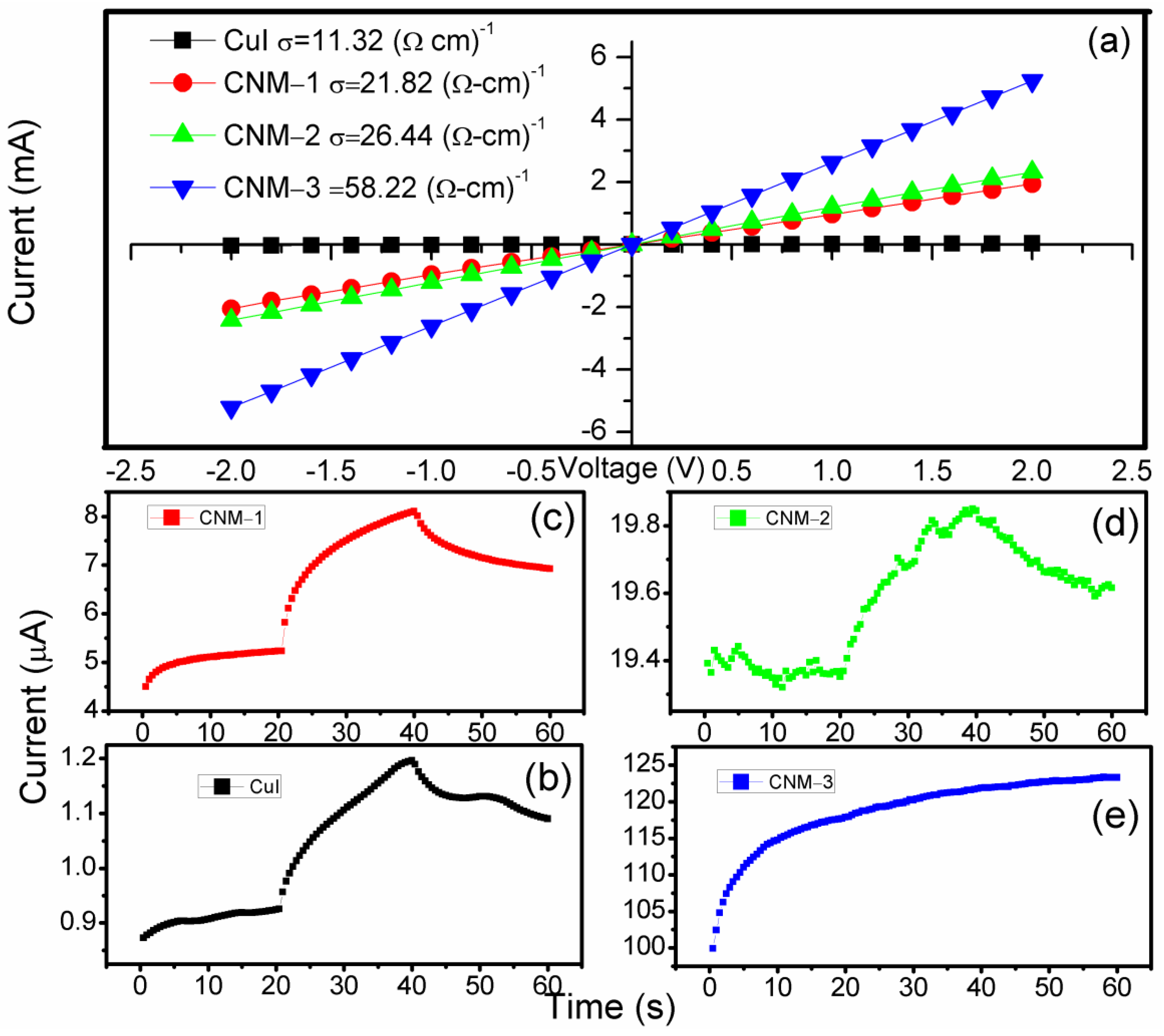
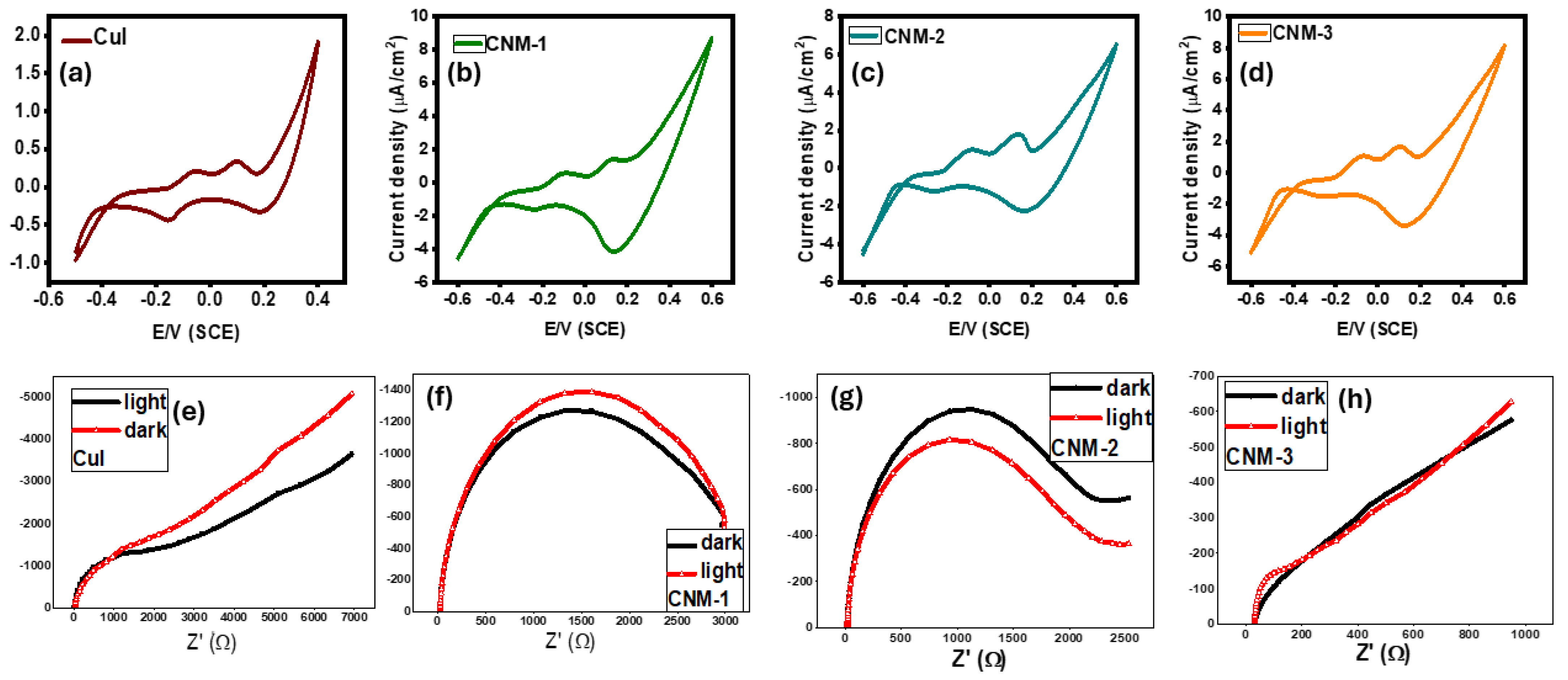
3.5. Photoelectrochemical Characterization

Figure 11 shows the DC photoresponse and the DC I-V curves of samples CNM-1, CNM-2, and CNM-3 and pure CuI. The photoresponse was obtained using a 30 W blue LED with an applied bias of 1 V. In the I-V curves, the conductivity of the samples is increased from 21 (Ω·cm)−1 to 58 (Ω·cm)−1. The value of the conductivity of base CuI is in the range of a few tens to hundreds of (Ω·cm)−1 [62]. This value can be increased to 200 by doping with Se [63]. Our method allows for an increase in conductivity without doping, which can lead to a detrimental effect when doping with high concentrations of atoms. The photoresponse of the films is evaluated at a 1 V bias voltage. It can be observed that upon illumination with the blue LED, the current increases from 0.9 μA to 1.2 μA. There is an evident increase in photocurrent when adding the composite material to CuI, to a highest value of 19.8 μA. Wang and co-workers demonstrated a p-CuI/n-Si heterojunction photodetector doped with Zn. Their results show that upon illumination with a UV light source of 325 nm, there is was increase in photocurrent due to the built-in heterojunction and rectifying behavior. However, some pin-holes were still present on the surface of the samples. Also, the single-step deposition of their CuI thin films allowed for faster crystallization, which led to inhomogeneities and hindered electrical performance [52]. Our work allows for a UV photodetector without the need for a Si substrate, which offers an evident advantage over what is normally reported in the literature, for example, a heterojunction based on TiO2 and Si [54,64]. There is a considerable increase in current for sample CNM-3 due to the increase in the conductivity value, which saturates the photogenerated charge carriers. During our experiments, the conductivity of CuI was enhanced due to the presence of MoS2 in the film. The composite allows for a heterojunction between g-C3N4 and MoS2. When more MoS2 is added to the thin film, charge extraction is enhanced due to the contact between CuI and MoS2 [65]. Increasing the concentration of MoS2 yields bigger crystals on top of the surface of CuI, which can contribute more charge carriers that can be extracted upon applying the bias. For comparison, samples were prepared with g-C3N4 and MoS2. It is observed that adding the materials separately does not enhance the photoconductivity of the base CuI film, which demonstrates that the composite enhances electrical behavior. These results can be found in the Supplementary File (Figure S3).
Figure 12 shows the photoelectrochemical characterization of all the samples. Figure 12a presents the cyclic voltammogram of the CuI film in a 0.5 M KCl electrolyte, revealing four characteristic electrochemical features. Upon immersion in the aqueous electrolyte, the surface oxidation of the CuI film may occur, potentially leading to the formation of Cu(II) species. In the cathodic scan, two peaks are observed at approximately +0.2 V and −0.2 V vs. SCE. The peak at +0.2 V could correspond to the reduction of Cu(II) to Cu(I), suggesting a residual oxygen reduction or adsorption process [66]. The peak at −0.2 V is consistent with the reduction of Cu(I) to Cu(0). In the subsequent anodic scan, oxidation processes occur, including the oxidation of Cu(0) to Cu(I) and the oxidation of I to I2 [67,68]. These processes result in quasi-reversible electrochemical behavior. The oxidation states observed in the CV are consistent with the results obtained from XPS analysis. Figure 12b, Figure 12c and Figure 12d correspond to the cyclic voltammogram of the CNM-1, CNM-2, and CNM-3 films, respectively. A higher current was obtained in CNM-1, CNM2, and CNM-3 than in CuI, suggesting an improved charge transfer process. In the anodic direction, peaks corresponding to Cu(0)/Cu(I) and I/I2 were observed, consistent with the cyclic voltammogram of pure CuI. Notably, a broad peak was observed at approximately −0.2 V/SCE in the CNM samples. To elucidate the involved process, cyclic voltammetry was carried out on CuI@g-C3N4 and CuI@MoS reference films (Figure S4a,b), revealing that the CuI profile is more pronounced in CuI@g-C3N4 than CuI@MoS2. This possibly suggests a stronger interaction between CuI and g-C3N4 owing to the presence of triazine rings and π-π interactions from g-C3N4, which contribute to a redistribution of charge density at the Cu sites, requiring higher potentials for oxidation. Conversely, the Mo-S bond in CuI@MoS₂, as revealed by Mo 3d and S 2p spectra in XPS analysis, may facilitate charge transfer and lower oxidation potentials in CuI@MoS2. Electrochemical impedance spectroscopy (EIS) was performed under dark and light conditions to investigate charge transfer resistance and separation. Nyquist plots, depicting the real impedance (Z′) on the x-axis and the imaginary impedance (Z″) on the y-axis, are presented in Figure 12e–h, as well as Figure S4c,d. The reference films, CuI@g-C3N4 and CuI@MoS2 (Figure S4c,d), displayed resistive behavior. Notably, CuI@g-C3N4 exhibited an increased impedance at low frequencies under illumination compared to dark conditions. This suggests a reduced charge transfer rate, potentially due to enhanced electron–hole recombination before charge transport. In contrast, CuI@MoS2, with its ~1.8 eV band gap and semi-metallic character, showed minimal changes between dark and light conditions, likely due to its high charge carrier density. The CuI and CNM-1 films (Figure 12e) displayed a Nyquist profile similar to g-C3N4, indicating rapid charge recombination. However, CNM-1 exhibited a lower intrinsic resistance, suggesting that the composite enhanced charge transport. Interestingly, CNM-2 films, composed of CuI@g-C3N4/MoS2 with 3% MoS2, demonstrated improved charge separation, as evidenced by a reduced arc under illumination, indicating less charge recombination. Conversely, CNM-3, with 5% MoS2, showed no significant change in its Nyquist profile, potentially due to the increased MoS2 content imparting more prominent semi-metallic characteristics.

4. Discussion

As already mentioned, adding g-C3N4/MoS2 composites enhances the conductivity of CuI. Similar results can be obtained by doping the thin films with elements like Se, in which case only DC conductivity is increased to almost 200 (Ω·cm)−1. In terms of the application of these films, they can be used as counter electrodes or transparent p-type semiconductors. In our case, the moderate conductivity values permit us to apply this material as a hole transport material in perovskite solar cells and as an efficient photocatalyst since the optical absorption is increased. Compared to the pure CuI thin films, which rely only on Cu vacancies for this purpose, the composite provides active sites for the photocatalytic process. Also, as the impedance spectroscopy measurements revealed, the heterojunction between g-C3N4/MoS2 and CuI enhances electron transfer upon illumination. Photoconductivity can be modulated by varying the concentration of MoS2.

5. Conclusions

In conclusion, CuI@g-C3N4/MoS2 hybrid thin films have been synthesized for the first time. A combination of thermal evaporation and a simple chemical method was used for synthesis. The crystalline structure of the CuI thin film is not changed upon the addition of the composite. g-C3N4/MoS2 is distributed on the surface of the films in the form of agglomerated particles, which allows for enhanced optical absorption. The material’s band gap is extended into the visible region when the concentration of MoS2 in the composite colloidal suspension is modulated. Therefore, the electrical and electrochemical properties of the films can be easily modulated by varying the concentration of this material. The addition of the composite enhances electron transport and injection from CuI, which allows it to be applied as a photocatalyst and as a hole transport material in perovskite solar cells.

Supplementary Materials

The following supporting information can be downloaded at https://www.mdpi.com/article/10.3390/photochem5010009/s1, Figure S1: HRTEM micrograph of g-C3N4/MoS2 composite of sample CNM-3, (b) SAED pattern of micrograph of CuI@ g-C3N4/MoS2 of sample CNM-3.; Figure S2: derivative of the absorbance with respect to wavelength vs wavelength for all the samples; Figure S3: DC photocurrent response for samples CuI@g-C3N4 and CuI@MoS2; Figure S4: Cyclic voltammogram and Nyquist graph for (a) and (c) g-C3N4@CuI and (b) and (d) MoS2@CuI, respectively

Author Contributions

Conceptualization: D.A.A.L. and M.Á.G.P. Data curation: D.A.A.L., C.R.S.R., and M.Á.G.P. Writing original draft: D.A.A.L. Supervision: M.Á.G.P. and S.S. Project administration and funding acquisition: M.Á.G.P. Resources: B.K., D.A.A., J.A.A.M., S.L.L., and A.E.R. Writing—reviewing and editing: D.A.A.L., C.R.S.R., N.A.R.D., S.S., B.K., D.A.A., J.A.A.M., S.L.L., A.E.R., and M.Á.G.P. All authors have read and agreed to the published version of the manuscript. All authors have read and approved the final version.

Funding

This research was funded by Autonomous University of Nuevo Leon, Mexico, under the PROACTII-UANL project PROACTI 128-FMYCT-2024.

Data Availability Statement

Dataset available on request from the authors

Acknowledgments

The authors acknowledge Facultad de Ciencias Físico Matemáticas, Facultad de Ingeniería Mecánica y Eléctrica, Centro de Investigación en Química Aplicada, and Centro de Investigación en Ingeniería Aeronáutica for providing the physical space and resources for this research. Two authors, Daniel A. Acuña Leal and Claudia R. Santiago Ramirez, acknowledge CONAHCYT for providing post-doctoral fellowship. The authors acknowledge the illustrator Ashley Yetzebel Caro Nava for providing the graphical abstract of this work.

Conflicts of Interest

The authors declare no conflicts of interest.

References

  1. Zhu, H.; Shin, E.-S.; Liu, A.; Ji, D.; Xu, Y.; Noh, Y.-Y. Printable Semiconductors for Backplane TFTs of Flexible OLED Displays. Adv. Funct. Mater. 2020, 30, 1904588. [Google Scholar] [CrossRef]
  2. Kawazoe, H.; Yasukawa, M.; Hyodo, H.; Kurita, M.; Yanagi, H.; Hosono, H. P-type electrical conduction in transparent thin films of CuAlO2. Nature 1997, 389, 939–942. [Google Scholar] [CrossRef]
  3. Sato, H.; Minami, T.; Takata, S.; Yamada, T. Transparent conducting p-type NiO thin films prepared by magnetron sputtering. Thin Solid Film 1993, 236, 27–31. [Google Scholar] [CrossRef]
  4. Moreira, M.; Afonso, J.; Crepelliere, J.; Lenoble, D.; Lunca-Popa, P. A review on the p-type transparent Cu–Cr–O delafossite materials. J. Mater. Sci. 2022, 57, 3114–3142. [Google Scholar] [CrossRef]
  5. Zhang, N.; Sun, J.; Gong, H. Transparent p-Type Semiconductors: Copper-Based Oxides and Oxychalcogenides. Coatings 2019, 9, 137. [Google Scholar] [CrossRef]
  6. Liu, A.; Zhu, H.; Noh, Y.-Y. Molecule Charge Transfer Doping for p-Channel Solution-Processed Copper Oxide Transistors. Adv. Funct. Mater. 2020, 30, 2002625. [Google Scholar] [CrossRef]
  7. Liu, A.; Zhu, H.; Kim, M.-G.; Kim, J.; Noh, Y.-Y. Engineering Copper Iodide (CuI) for Multifunctional p-Type Transparent Semiconductors and Conductors. Adv. Sci. 2021, 8, 2100546. [Google Scholar] [CrossRef]
  8. Storm, P.; Bar, M.S.; Selle, S.; von Wenckstern, H.; Grundmann, M.; Lorenz, M. p-Type Doping and Alloying of CuI Thin Films with Selenium. Phys. Status Solidi (RRL) Rapid Res. Lett. 2021, 15, 2100214. [Google Scholar] [CrossRef]
  9. Kaushik, D.K.; Selvaraj, M.; Ramu, S.; Subrahmanyam, A. Thermal evaporated Copper Iodide (CuI) thin films: A note on the disorder evaluated through the temperature dependent electrical properties. Sol. Energy Mater. Sol. Cells 2017, 165, 52–58. [Google Scholar] [CrossRef]
  10. Ayhan, M.E.; Shinde, M.; Todankar, B.; Desai, P.; Ranade, A.K.; Tanemura, M.; Kalita, G. Ultraviolet radiation-induced photovoltaic action in γ-CuI/β-Ga2O3 heterojunction. Mater. Lett. 2020, 262, 127074. [Google Scholar] [CrossRef]
  11. Kim, T.; Son, C.; Lee, J.; Oh, E.; Li, S.; Chang, C.-H.; Lim, S. Interfacial ZnS passivation for improvement of transparent ZnO/CuI diode characteristics. Appl. Surf. Sci. 2021, 536, 147645. [Google Scholar] [CrossRef]
  12. Lee, J.H.; Lee, W.-J.; Kim, T.H.; Lee, T.; Hong, S.; Kim, K.H. Transparent p-CuI/n-BaSnO3−δ heterojunctions with a high rectification ratio. J. Phys. Condens. Matter 2017, 29, 384004. [Google Scholar] [CrossRef]
  13. Lee, J.H.; Lee, B.H.; Kang, J.; Diware, M.; Jeon, K.; Jeong, C.; Lee, S.Y.; Kim, K.H. Characteristics and Electronic Band Alignment of a Transparent p-CuI/n-SiZnSnO Heterojunction Diode with a High Rectification Ratio. Nanomaterials 2021, 11, 1237. [Google Scholar] [CrossRef] [PubMed]
  14. Cha, J.-H.; Jung, D.-Y. Air-Stable Transparent Silver Iodide–Copper Iodide Heterojunction Diode. ACS Appl. Mater. Interfaces 2017, 9, 43807–43813. [Google Scholar] [CrossRef]
  15. Annadi, A.; Zhang, N.; Boon Kiang Lim, D.; Gong, H. New Transparent Magnetic Semiconductor NixCu1–xI which Can Perform as Either P-type or N-type and Success in the P–N Homojunction Diode. ACS Appl. Mater. Interfaces 2020, 12, 6048–6055. [Google Scholar] [CrossRef]
  16. Antoniadou, M.; Arfanis, M.K.; Ibrahim, I.; Falaras, P. Bifunctional g-C3N4/WO3 Thin Films for Photocatalytic Water Purification. Water 2019, 11, 2439. [Google Scholar] [CrossRef]
  17. Bu, Y.; Chen, Z.; Yu, J.; Li, W. A novel application of g-C3N4 thin film in photoelectrochemical anticorrosion. Electrochim. Acta 2013, 88, 294–300. [Google Scholar] [CrossRef]
  18. Nagal, V.; Kumar, V.; Ahmad, R.; Khan, M.; Khan, Z.H.; Singh, K.; Furukawa, H.; Khosla, A.; Hahn, Y.B.; Hafiz, A.K. Review—Emerging Applications of g-C3N4 Films in Perovskite-Based Solar Cells. ECS J. Solid State Sci. Technol. 2021, 10, 065001. [Google Scholar] [CrossRef]
  19. Sangiorgi, N.; Tuci, G.; Sanson, A.; Peruzzini, M.; Giambastiani, G. Metal-free carbon-based materials for electrocatalytic and photo-electrocatalytic CO2 reduction. Rend. Lincei. Sci. Fis. E Nat. 2019, 30, 497–513. [Google Scholar] [CrossRef]
  20. Chen, F.; Wu, C.; Zheng, G.; Qu, L.; Han, Q. Few-layer carbon nitride photocatalysts for solar fuels and chemicals: Current status and prospects. Chin. J. Catal. 2022, 43, 1216–1229. [Google Scholar] [CrossRef]
  21. Chen, L.; Yan, G.; Liu, X.; Ying, S.; Xia, Y.; Ning, S.; Wang, X. Phosphorus doped and defect modified graphitic carbon nitride for boosting photocatalytic hydrogen production. Phys. Chem. Chem. Phys. 2023, 25, 117–123. [Google Scholar] [CrossRef] [PubMed]
  22. Dong, J.; Zhang, Y.; Hussain, M.I.; Zhou, W.; Chen, Y.; Wang, L.-N. g-C3N4: Properties, Pore Modifications, and Photocatalytic Applications. Nanomaterials 2022, 12, 121. [Google Scholar] [CrossRef] [PubMed]
  23. Muchuweni, E.; Mombeshora, E.T.; Martincigh, B.S.; Nyamori, V.O. Graphitic carbon nitride-based new-generation solar cells: Critical challenges, recent breakthroughs and future prospects. Sol. Energy 2022, 239, 74–87. [Google Scholar] [CrossRef]
  24. Acuña Leal, D.A.; Santiago Ramírez, C.R.; Ramos Delgado, N.A.; Shaji, S.; Gracia Pinilla, M.A. Graphitic carbon nitride hybrid thin films for energy conversion: A mini-review on defect activation with different materials. Nanotechnol. Rev. 2024, 13, 20240127. [Google Scholar] [CrossRef]
  25. Mamba, G.; Mishra, A.K. Graphitic carbon nitride (g-C3N4) nanocomposites: A new and exciting generation of visible light driven photocatalysts for environmental pollution remediation. Appl. Catal. B Environ. 2016, 198, 347–377. [Google Scholar] [CrossRef]
  26. Samy, O.; Zeng, S.; Birowosuto, M.D.; El Moutaouakil, A. A Review on MoS2 Properties, Synthesis, Sensing Applications and Challenges. Crystals 2021, 11, 355. [Google Scholar] [CrossRef]
  27. Shi, L.; He, Z.; Liu, S. MoS2 quantum dots embedded in g-C3N4 frameworks: A hybrid 0D-2D heterojunction as an efficient visible-light driven photocatalyst. Appl. Surf. Sci. 2018, 457, 30–40. [Google Scholar] [CrossRef]
  28. Ansari, S.A.; Cho, M.H. Simple and Large Scale Construction of MoS2-g-C3N4 Heterostructures Using Mechanochemistry for High Performance Electrochemical Supercapacitor and Visible Light Photocatalytic Applications. Sci. Rep. 2017, 7, 43055. [Google Scholar] [CrossRef]
  29. Zheng, H.; Sun, X.; Liu, Y.; Jiang, S.; Wang, D.; Fan, Y.; Hu, L.; Zhang, D.; Yao, W.; Zhang, L. New g-C3N4/GO/MoS2 composites as efficient photocatalyst for photocathodic protection of 304 stainless steel. Water Sci. Technol. 2021, 84, 499–511. [Google Scholar] [CrossRef]
  30. Ye, L.; Wang, D.; Chen, S. Fabrication and Enhanced Photoelectrochemical Performance of MoS2/S-Doped g-C3N4 Heterojunction Film. ACS Appl. Mater. Interfaces 2016, 8, 5280–5289. [Google Scholar] [CrossRef]
  31. Liu, Y.; Chen, L.; Liu, X.; Qian, T.; Yao, M.; Liu, W.; Ji, H. Tuning band structure of graphitic carbon nitride for efficient degradation of sulfamethazine: Atmospheric condition and theoretical calculation. Chin. Chem. Lett. 2022, 33, 1385–1389. [Google Scholar] [CrossRef]
  32. Tan, X.; Kou, L.; Tahini, H.A.; Smith, S.C. Conductive Graphitic Carbon Nitride as an Ideal Material for Electrocatalytically Switchable CO2 Capture. Sci. Rep. 2015, 5, 17636. [Google Scholar] [CrossRef] [PubMed]
  33. Sun, M.; He, Z.-L.; Yuan, C.; Wang, X.; Zhai, C.; Zhu, M. Heterostructures Based on g-C3N4/CuI as a Photoactivated Support for Pt Nanoparticles toward Efficient Photoelectrocatalytic Methanol Oxidation. Ind. Eng. Chem. Res. 2021, 60, 762–770. [Google Scholar] [CrossRef]
  34. Meftahi, A.; Reisi-Vanani, A.; Shabani-Nooshabadi, M. Comparison of performance of CuI/g-C3N4 nanocomposites synthesized on Ni-foam and graphitic substrates as suitable electrode materials for supercapacitors. Fuel 2023, 331, 125683. [Google Scholar] [CrossRef]
  35. Rugma, T.P.; Lakhera, S.K.; Sahoo, T.; Neppolian, B. Phosphorus modified and CuI incorporated polymeric g-C3N4 photocatalyst for efficient photocatalytic hydrogen production under direct solar light irradiation. Mater. Sci. Eng. B 2022, 284, 115873. [Google Scholar] [CrossRef]
  36. Peng, W.; Li, L.; Yu, S.; Zheng, H.; Yang, P. Structure, binding energy and optoelectrical properties of p-type CuI thin films: The effects of thickness. Appl. Surf. Sci. 2020, 502, 144424. [Google Scholar] [CrossRef]
  37. Fina, F.; Callear, S.K.; Carins, G.M.; Irvine, J.T.S. Structural Investigation of Graphitic Carbon Nitride via XRD and Neutron Diffraction. Chem. Mater. 2015, 27, 2612–2618. [Google Scholar] [CrossRef]
  38. Li, Z.; Zhang, L.; Wang, J.; Yang, L.; Xin, L.; Li, G.; Lin, G.; Niu, S.; Yan, J.; Zhao, F. Hydrothermal growth and their optoelectronic device application of CuI nanostructure. Mater. Res. Express 2019, 6, 045048. [Google Scholar] [CrossRef]
  39. Kim, H.-J.; Kim, D.; Jung, S.; Bae, M.-H.; Yun, Y.J.; Yi, S.N.; Yu, J.-S.; Kim, J.-H.; Ha, D.H. Changes in the Raman spectra of monolayer MoS2 upon thermal annealing. J. Raman Spectrosc. 2018, 49, 1938–1944. [Google Scholar] [CrossRef]
  40. Bagnall, A.G.; Liang, W.Y.; Marseglia, E.A.; Welber, B. Raman studies of MoS2 at high pressure. Phys. B+C 1980, 99, 343–346. [Google Scholar] [CrossRef]
  41. Lee, C.; Yan, H.; Brus, L.E.; Heinz, T.F.; Hone, J.; Ryu, S. Anomalous Lattice Vibrations of Single- and Few-Layer MoS2. ACS Nano 2010, 4, 2695–2700. [Google Scholar] [CrossRef]
  42. Allred, A.L. Electronegativity values from thermochemical data. J. Inorg. Nucl. Chem. 1961, 17, 215–221. [Google Scholar] [CrossRef]
  43. Posopa, N.; Sakulkalavek, A.; Chanlek, N.; Kaewkhao, J.; Sakdanuphab, R. Room-temperature rapid synthesis of CuI thin films via liquid iodination method. Superlattices Microstruct. 2020, 141, 106501. [Google Scholar] [CrossRef]
  44. Chinnakutti, K.K.; Panneerselvam, V.; Govindarajan, D.; Soman, A.K.; Parasuraman, K.; Thankaraj Salammal, S. Optoelectronic and electrochemical behaviour of γ-CuI thin films prepared by solid iodination process. Prog. Nat. Sci. Mater. Int. 2019, 29, 533–540. [Google Scholar] [CrossRef]
  45. Sharma, P.; Sarngan, P.P.; Lakshmanan, A.; Sarkar, D. One-step synthesis of highly reactive g-C3N4. J. Mater. Sci. Mater. Electron. 2022, 33, 9116–9125. [Google Scholar] [CrossRef]
  46. Li, B.; Jiang, L.; Li, X.; Ran, P.; Zuo, P.; Wang, A.; Qu, L.; Zhao, Y.; Cheng, Z.; Lu, Y. Preparation of Monolayer MoS2 Quantum Dots using Temporally Shaped Femtosecond Laser Ablation of Bulk MoS2 Targets in Water. Sci. Rep. 2017, 7, 11182. [Google Scholar] [CrossRef] [PubMed]
  47. Moulder, J.F.; Chastain, J. Handbook of X-ray Photoelectron Spectroscopy: A Reference Book of Standard Spectra for Identification and Interpretation of XPS Data; Physical Electronics Division, Perkin-Elmer Corporation: Waltham, MA, USA, 1992. [Google Scholar]
  48. Ahn, K.; Kim, G.H.; Kim, S.-J.; Kim, J.; Ryu, G.-S.; Lee, P.; Ryu, B.; Cho, J.Y.; Kim, Y.-H.; Kang, J.; et al. Highly Conductive p-Type Transparent Conducting Electrode with Sulfur-Doped Copper Iodide. Chem. Mater. 2022, 34, 10517–10527. [Google Scholar] [CrossRef]
  49. Zheng, Y.; Zhang, Z.; Li, C. A comparison of graphitic carbon nitrides synthesized from different precursors through pyrolysis. J. Photochem. Photobiol. A Chem. 2017, 332, 32–44. [Google Scholar] [CrossRef]
  50. Gowri, V.M.; Ajith, A.; John, S.A. Systematic Study on Morphological, Electrochemical Impedance, and Electrocatalytic Activity of Graphitic Carbon Nitride Modified on a Glassy Carbon Substrate from Sequential Exfoliation in Water. Langmuir 2021, 37, 10538–10546. [Google Scholar] [CrossRef]
  51. Nasir, S.N.S.; Mohamed, N.A.; Tukimon, M.A.; Noh, M.F.M.; Arzaee, N.A.; Teridi, M.A.M. Direct extrapolation techniques on the energy band diagram of BiVO4 thin films. Phys. B Condens. Matter 2021, 604, 412719. [Google Scholar] [CrossRef]
  52. Wang, M.; Zhuang, M.; Ge, L.; Yuan, Y.; Wang, Z.; Liu, W.; Li, H.; Song, A. Tunable photoresponse properties of CuI/Si self-powered photodetectors through Zn doping engineering. Appl. Surf. Sci. 2024, 654, 159400. [Google Scholar] [CrossRef]
  53. Geng, F.; Yang, L.; Dai, B.; Guo, S.; Gao, G.; Xu, L.; Han, J.; Bolshakov, A.; Zhu, J. Enhanced transmittance and mobility of p-type copper iodide thin films prepared at room temperature via a layer-by-layer approach. Surf. Coat. Technol. 2019, 361, 396–402. [Google Scholar] [CrossRef]
  54. Huang, Y.; Tan, J.; Gao, G.; Xu, J.; Zhao, L.; Zhou, W.; Wang, Q.; Yuan, S.; Sun, J. Transparent p-type CuI film based self-powered ultraviolet photodetectors with ultrahigh speed, responsivity and detectivity. J. Mater. Chem. C 2022, 10, 13040–13046. [Google Scholar] [CrossRef]
  55. Xue, Z.; Zhang, X.; Qin, J.; Liu, R. Constructing MoS2/g-C3N4 heterojunction with enhanced oxygen evolution reaction activity: A theoretical insight. Appl. Surf. Sci. 2020, 510, 145489. [Google Scholar] [CrossRef]
  56. Li, Z.H.; He, J.X.; Lv, X.H.; Chi, L.F.; Egbo, K.O.; Li, M.-D.; Tanaka, T.; Guo, Q.X.; Yu, K.M.; Liu, C.P. Optoelectronic properties and ultrafast carrier dynamics of copper iodide thin films. Nat. Commun. 2022, 13, 6346. [Google Scholar] [CrossRef]
  57. Senthilnathan, S.; Kumar, K.G.; Sugunraj, S.; Dhanalakshmi, M.A.; Rajendraprasad, M.; Suganthi, M.; Kesavan, K.S.; Sasikumar, P.; Abbas, M.; Dator, W.L.T. MoS2 modified g-C3N4 composite: A potential candidate for photocatalytic applications. J. Saudi Chem. Soc. 2023, 27, 101717. [Google Scholar] [CrossRef]
  58. Bosch Ojeda, C.; Sanchez Rojas, F. Recent developments in derivative ultraviolet/visible absorption spectrophotometry. Anal. Chim. Acta 2004, 518, 1–24. [Google Scholar] [CrossRef]
  59. Trenczek-Zajac, A.; Synowiec, M.; Zakrzewska, K.; Zazakowny, K.; Kowalski, K.; Dziedzic, A.; Radecka, M. Scavenger-Supported Photocatalytic Evidence of an Extended Type I Electronic Structure of the TiO2@Fe2O3 Interface. ACS Appl. Mater. Interfaces 2022, 14, 38255–38269. [Google Scholar] [CrossRef]
  60. Moditswe, C.; Muiva, C.M.; Luhanga, P.; Juma, A. Effect of annealing temperature on structural and optoelectronic properties of γ-CuI thin films prepared by the thermal evaporation method. Ceram. Int. 2017, 43, 5121–5126. [Google Scholar] [CrossRef]
  61. Wang, R.; Wang, Y.; Mao, S.; Hao, X.; Duan, X.; Wen, Y. Different Morphology MoS2 Over the g-C3N4 as a Boosted Photo-Catalyst for Pollutant Removal Under Visible-Light. J. Inorg. Organomet. Polym. Mater. 2021, 31, 32–42. [Google Scholar] [CrossRef]
  62. Rahman, M.; Newaz, M.A.; Mondal, B.K.; Kuddus, A.; Karim, M.A.; Rashid, M.M.; Rubel, M.H.K.; Hossain, J. Unraveling the electrical properties of solution-processed copper iodide thin films for CuI/n-Si solar cells. Mater. Res. Bull. 2019, 118, 110518. [Google Scholar] [CrossRef]
  63. Zhou, Z.; Liu, R.; Yang, Y.; Zheng, Y.; Wei, B.; Zhang, W.; Zou, M.; Han, J.; Liu, Y.; Lan, J.; et al. Synergistic effects of CuI doping on enhancing thermoelectric performance for n-type Bi2O2Se fabricated by mechanical alloying. Scr. Mater. 2023, 225, 115163. [Google Scholar] [CrossRef]
  64. Zuo, C.; Cai, S.; Li, Z.; Fang, X. A transparent, self-powered photodetector based on p-CuI/n-TiO2 heterojunction film with high on–off ratio. Nanotechnology 2022, 33, 105202. [Google Scholar] [CrossRef]
  65. Mahyavanshi, R.D.; Desai, P.; Ranade, A.; Tanemura, M.; Kalita, G. Observing Charge Transfer Interaction in CuI and MoS2 Heterojunction for Photoresponsive Device Application. ACS Appl. Electron. Mater. 2019, 1, 302–310. [Google Scholar] [CrossRef]
  66. Konakov, A.O.; Dremova, N.N.; Khodos, I.I.; Koch, M.; Zolotukhina, E.V.; Silina, Y.E. One-Pot Synthesis of Copper Iodide-Polypyrrole Nanocomposites. Chemosensors 2021, 9, 56. [Google Scholar] [CrossRef]
  67. Kosta, I.; Azaceta, E.; Yate, L.; Cabañero, G.; Grande, H.; Tena-Zaera, R. Cathodic electrochemical deposition of CuI from room temperature ionic liquid-based electrolytes. Electrochem. Commun. 2015, 59, 20–23. [Google Scholar] [CrossRef]
  68. Ghazal, N.; Madkour, M.; Abdel Nazeer, A.; Obayya, S.S.A.; Mohamed, S.A. Electrochemical capacitive performance of thermally evaporated Al-doped CuI thin films. RSC Adv. 2021, 11, 39262–39269. [Google Scholar] [CrossRef]
Figure 1. X-ray diffraction pattern of CNM-1, CNM-2, and CNM-3 samples. A sample of pure CuI is also shown in the figure for comparison.
Photochem 05 00009 g001
Figure 2. Raman spectra of samples CNM-1, CNM-2, and CNM-3. For comparison, a pure CuI sample is also presented.
Photochem 05 00009 g002
Figure 3. Raman spectra of the bulk MoS2 sample.
Photochem 05 00009 g003
Figure 4. (a) XPS survey spectra of the powders of g-C3N4 and MoS2; (b) high-resolution spectra for the C 1s and N 1s core levels for carbon nitride, and Mo 3d and S 2p for MoS2. The experimental data is marked with black open circles, the Shirley background is marked with a green line, the photoelectron fitted peaks are marked in red and the total fitted curve is marked in blue.
Photochem 05 00009 g004
Figure 5. Survey spectra of all the CuI@MoS2/g-C3N4 thin films.
Photochem 05 00009 g005
Figure 6. XPS high-resolution spectra of the core levels of: (a) C 1s, (b) N 1s, (c) Mo 3d, (d) S 2p, (e) Cu 2p, and (f) I 3d for samples CNM-1, CNM-2, and CNM-3, respectively. The experimental data is marked with black open circles, the Shirley background is marked with a green line, the photoelectron fitted peaks are marked in red and the total fitted curve is marked in blue.
Photochem 05 00009 g006
Figure 7. Valence band XPS spectra for pure g-C3N4, MoS2, CuI, and samples CNM-1, CNM-2, and CNM-3, respectively. The solid line is the extrapolation from the valence band edge. The dashed line is the extrapolation from the baseline. The black solid line is the experimental data.
Photochem 05 00009 g007
Figure 8. (a) SEM micrograph of pure CuI thin film, (b) SEM micrograph of sample CNM-1, (c) SEM micrograph of sample CNM-2, (d) SEM micrograph of sample CNM−3, (e) TEM micrograph of g-C3N4/MoS2 composite of sample CNM-3, and (f) TEM micrograph of CuI@g-C3N4/MoS2 of sample CNM−3.
Photochem 05 00009 g008
Figure 9. Absorption spectra of samples CNM-1, CNM-2, and CNM-3. For comparison, the absorption spectra of a pure CuI thin film is also presented.
Photochem 05 00009 g009
Figure 10. Tauc Plots of samples CNM-1, CNM-2, and CNM-3. For comparison, the Tauc Plot of a pure CuI sample is also presented. The red line is the extrapolation from the linear part of the Tauc Plot. The black dotted curve is the calculated Tauc plot.
Photochem 05 00009 g010
Figure 11. (a) IV curves and DC photoresponse curves of samples (b) CuI, (c) CNM-1, (d) CNM-2 and (e) CNM-3.
Photochem 05 00009 g011
Figure 12. Cyclic voltammograms and Nyquist graphs for (a,e) CuI, (b,f) CNM-1, (c,g) CNM-2, and (d,h) CNM-3 used for the photoelectrochemical characterization of the samples.
Photochem 05 00009 g012
Disclaimer/Publisher’s Note: The statements, opinions and data contained in all publications are solely those of the individual author(s) and contributor(s) and not of MDPI and/or the editor(s). MDPI and/or the editor(s) disclaim responsibility for any injury to people or property resulting from any ideas, methods, instructions or products referred to in the content.

