1. Introduction
Selenium (Se) has emerged as a promising photovoltaic material due to its unique combination of a wide bandgap (~1.7–1.95 eV) [
1,
2,
3,
4], high absorption coefficient (>10
5 cm
−1 in the visible spectrum), non-toxicity, and low melting point. In outdoor scenarios, it can function as an optimal top cell in tandem configuration [
5,
6,
7,
8], enabling broader utilization of the solar spectrum and surpassing the Shockley–Queisser efficiency limit for single-junction devices. Within indoor environments, where light intensity ranges from 100 to 1000 lux and is dominated by blue-rich wavelengths (400–700 nm), Se’s bandgap aligns with the optimal absorption range of LED and fluorescent light sources [
9,
10]. This makes Se a vital material for powering indoor Internet of Things (IoT) applications [
11,
12], including wireless sensors and electronic shelf labels, without relying on external energy sources. Additionally, Todorov et al. [
2] reported a Se solar cell efficiency of 2.7% using a 20 nm thick Se absorption layer, a feat that renders Se solar cells particularly appealing for applications such as power supplies in wearable devices and flexible electronics.
The properties of the Se absorption layer are pivotal for the performance of Se solar cells. Amorphous selenium (a-Se) exhibits extremely high electrical resistivity and short minority carrier lifetimes [
4], making it unsuitable for use as an absorption layer in solar cells. Thermal processing-induced crystallization triggers a structural transformation, with the trigonal phase emerging as the most thermodynamically stable crystalline form of selenium. In 1985, Nakada et al. [
13] deposited a 1.5 nm Te interfacial adhesion layer, followed by thermal evaporation of a-Se films. Subsequent annealing at 180–220 °C produced high-crystallinity selenium thin films. Using this methodology, they achieved a record-breaking power conversion efficiency of 5.01% in Se cells, establishing a foundational technical framework that continues to guide modern selenium-based solar cell fabrication [
1,
14,
15,
16,
17,
18]. Hadar et al. [
3] systematically investigated the influence of preparation conditions such as heating rate, Te layer thickness, and illumination effects during the crystallization process on device performance. Additionally, they explored the bandgap tunability of Se [
19], which promoted a broader application of Se-based solar cells. More recently, Xue et al. [
10] developed a critical melting–annealing (CMA) strategy to integrate disordered one-dimensional Se chains into the trigonal lattice, enabling Se solar cells to achieve certified efficiencies of 7.2% under AM1.5G illumination and 18.0% under 1000-lux indoor light. By optimizing a substrate-heating strategy to grow Se films perpendicular to the substrate, the device efficiency was further enhanced to 8.1% under AM1.5G illumination [
20]. Particularly, Xue’s group introduced a glue-bonding strategy using molten Se to fabricate bifacial Se solar cells, achieving a bifaciality factor of 90.1% and efficiencies of 8.61% under 1-sun illumination [
21]. Notably, all these studies relied on thermal evaporation for Se thin-film fabrication—which requires high-vacuum conditions and exhibits low throughput, thus rendering it unsuitable for the industrial-scale production of Se solar cells. Further exploration of low-cost, high-throughput fabrication techniques for Se thin films is therefore essential to facilitate their industrial implementation.
In this study, we present an innovative vapor transport deposition (VTD) technique for the fabrication of Se thin films. The VTD approach exploits a temperature gradient within a tubular furnace to induce the evaporation of selenium powder, which is then transported by a controlled nitrogen gas flow and condensed onto a cooler substrate. By modulating the carrier gas flow, VTD allows for precise control of the deposition rate, thereby enabling large-scale thin-film production under relatively lower vacuum conditions, which aligns well with the requirements for low-cost, high-efficiency manufacturing. This approach has already been extensively used in the fabrication of thin-film photovoltaics such as CdTe solar cells [
6,
22,
23,
24]. Through a systematic investigation of how substrate temperature influences Se film morphology, crystallinity, and optical properties, alongside an analysis of light/dark current density–voltage (J-V) characteristics and quantum efficiency (QE), this study demonstrates that VTD represents a promising strategy for scalable, cost-effective production of high-performance Se solar cells.
2. Materials and Methods
The preparation process flowchart of vapor transport-deposited Se thin-film solar cells is presented in
Figure 1a. Fluorine-doped tin oxide (FTO)-coated glass substrates (Tec15 from Pilkington) were ultrasonically cleaned prior to deposition. A TiO
2 electron transport layer was deposited on the FTO substrate via magnetron sputtering using a high-purity TiO
2 ceramic target (99.999%, Zhongnuo Advanced Materials Technology Co., Ltd., Beijing, China). The deposition process was conducted at 100 W power for 20 min, yielding a uniform film with a thickness of approximately 70 nm. Subsequently, the as-deposited TiO
2 film was annealed in a tubular furnace under ambient air conditions. The temperature was ramped up from room temperature to 550 °C at a rate of 4 °C/min and held at the peak temperature for 30 min. Following Nakada’s methodology [
13], an ultrathin Te adhesion layer (approximately 1.5 nm) was deposited by thermal evaporation using high-purity Te powder (99.999%, InnoChem Technology Co., Ltd., Beijing, China). For the preparation of the Se absorber layer, a novel homemade vapor transport deposition technique was employed. High-purity Se powder (99.999%, InnoChem Technology Co., Ltd.) was placed at the central zone of a quartz tube within a tubular annealing furnace. The quartz tube was evacuated to a base pressure of approximately 10
−1 Pa using a mechanical pump. Then, nitrogen gas (99.999%, Chongqing Zhongrong Gas Co., Ltd., Chongqing, China) was introduced as the carrier gas. A precisely controlled heating program was implemented; the furnace temperature was increased from room temperature to 300 °C at a ramp rate of 20 °C/min. During the heating process, the Se powder evaporated and was carried by the nitrogen flow to a cooler region of the tube. The condensed selenium formed thin films exhibiting thicknesses of approximately 660 nm at the hot-side central region and 350 nm at the cold-side central region. To investigate the impact of substrate temperature on the thin-film properties and device performance, substrates were placed at positions closer to and farther from the heat source, corresponding to substrate temperatures of ~165 and 95 °C, respectively. The Au back electrode was deposited using an ion-sputtering system under a working current of 1 mA for 400 s (~40 nm). Finally, the device underwent brief thermal annealing on a hotplate at 180 °C for 3 min to complete device fabrication. The device area was defined as 0.36 cm
2 using a stainless-steel mask.
The film thickness was determined by a profilometer (KLA Tencor D-600, KLA Inc., Milpitas, CA, USA). The structural properties of the films were analyzed via X-ray diffraction (TD-3500, Dandong Tongda Science and Technology Co., Ltd., Dandong, China) with Cu Ka radiation (λ = 1.54056 Å). Diffraction measurements were conducted over a 2θ range of 10°–80°. Optical transmission spectra were recorded employing a UV-Vis-NIR grating spectrophotometer (Shimadzu UV-3600i Plus, Shimadzu Inc., Kyoto, Japan) across a wavelength range of 300–1000 nm. Surface morphologies of the films were examined using a scanning electron microscope (Hitachi Regulus 8230, Hitachi High-Tech Inc., Kyoto, Japan). The current–voltage (I-V) characteristics of the solar cells were measured by using a cell tester (XJCM-9, Shaanxi Zhongshen Power Energy Technology Co., Ltd., Xi’an, China) under simulated AM1.5 sunlight at 100 mW/cm2 irradiation. QE measurement was performed by QEX10 (PV Measurements, Inc., Boulder, CO, USA) in the wavelength range of 300–1000 nm. The Keithley 2400 digital source meter was used in dark I-V measurement.
3. Results and Discussions
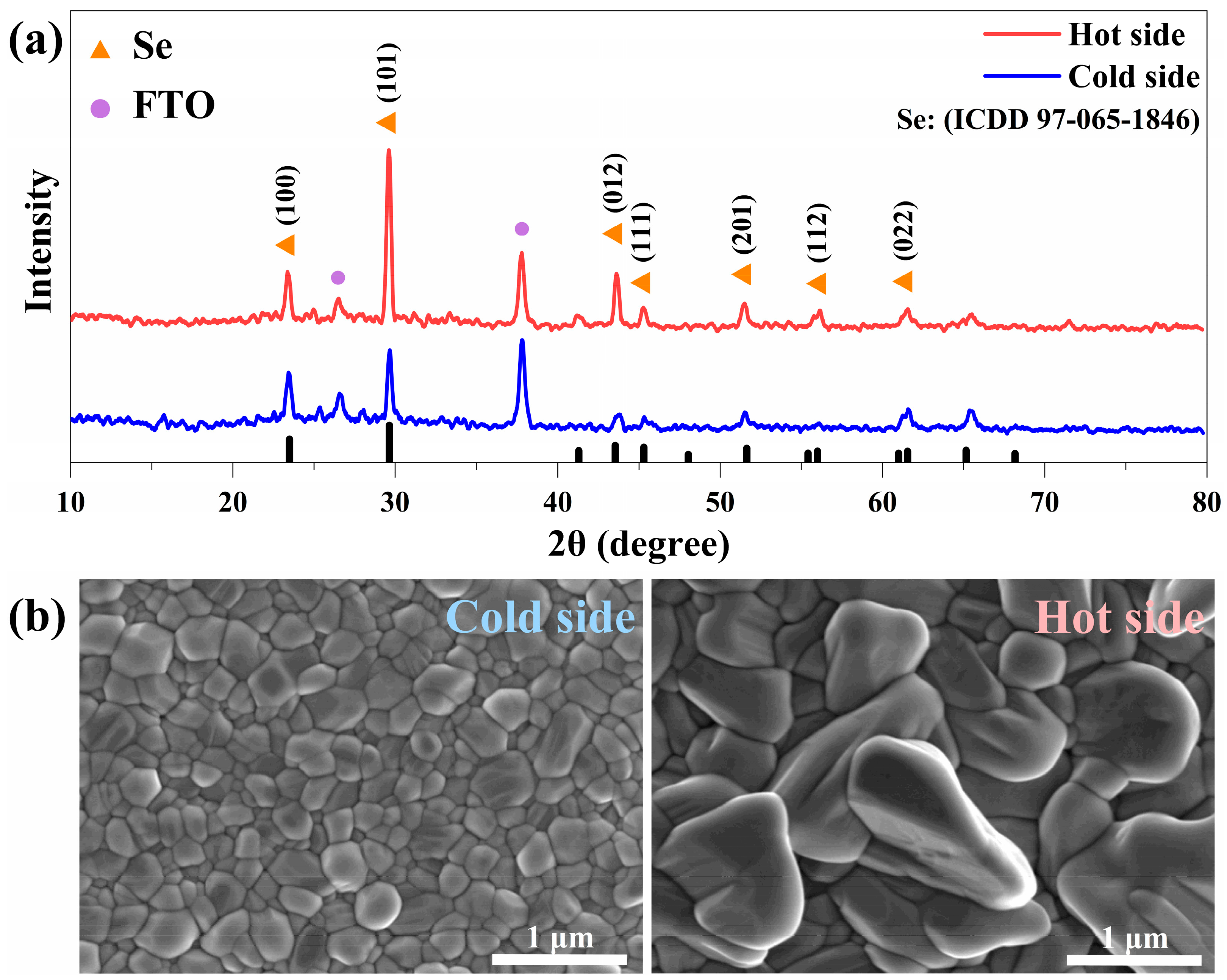
The structural properties of Se thin films deposited in hot-side and cold-side regions were systematically characterized using XRD. The as-deposited film obtained at the cold side showed no detectable diffraction peaks, while the hot-side counterpart exhibited distinct peaks at 23.4° (100), 29.6° (101), and 43.5° (012), as illustrated in
Figure S1 (Supporting Information), which is consistent with the hexagonal phase of selenium (ICDD 97-065-1846). Following 180 °C thermal annealing for 3 min, the cold-side film developed comparable diffraction patterns (see
Figure 2a), though with substantially lower peak intensities than the hot-side film. This thermal gradient-induced crystallinity difference originates from in situ annealing effects during deposition. The hot-side region’s proximity to the heating zone generated localized in situ annealing effects, promoting atomic rearrangement and the formation of larger, well-ordered crystalline domains.
SEM analysis further confirmed this structural evolution. The as-deposited Se film obtained at the cold side exhibits nanocrystalline particles, while the grains at the hot side are significantly larger, as illustrated in
Figure S2 (Supporting Information). Notably, the as-deposited Se film has sharp-edged grains, and after annealing at 180 °C, the surface consisted of rounded grains with penetrating boundaries and grain size reaching the micrometer scale, as illustrated in
Figure S3 (Supporting Information), indicative of thermally activated grain coalescence. Notably, we found that the Se films deposited at the hot side exhibited higher surface roughness than those at the cold side, as shown in
Figure 2b. This phenomenon may arise from the relatively shorter distance between the hot side and the Se source during deposition, which could lead to non-uniform particle distribution in the vapor transport process. The cross-sectional SEM image of the completed device with the hot-side Se absorber is also presented in
Figure 1b. It can be observed that the interfaces between layers are well-defined, and the annealed Se films exhibit a homogeneous and dense structure without cracks or voids. These studies demonstrated that the vapor transport deposition method can be utilized to fabricate dense and intact Se thin films.
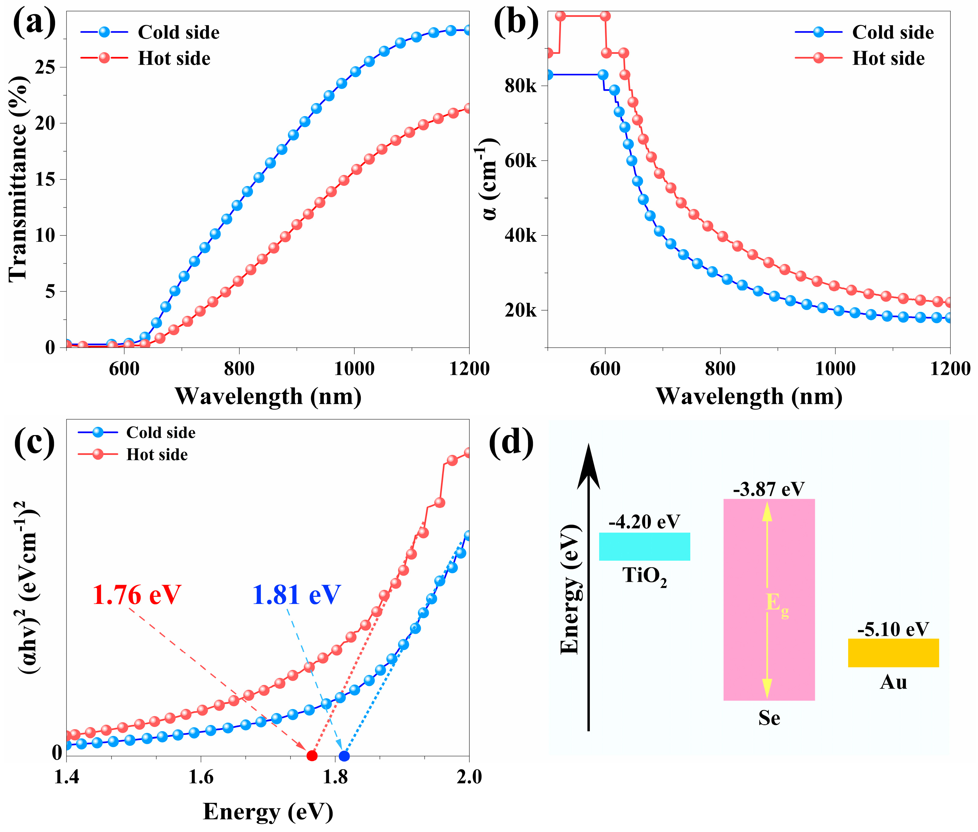
The optical properties of the vapor transport-deposited Se films annealed at 180 °C for 3 min were investigated through transmittance measurements. As depicted in
Figure 3a, the hot-side film exhibited lower transmittance in the 600–1200 nm wavelength range compared to the cold-side film, indicating enhanced light absorption. The absorption coefficient (
α) was calculated using Lambert–Beer’s Law.
where
d is the film thickness and
T is the transmittance. The absorption coefficients of the vapor transport-deposited Se films are showed in
Figure 3b.
The optical bandgap (
Eg) was determined using the Tauc plot method, expressed as
where
n = 2 for direct bandgap semiconductors. As shown in
Figure 3c, by plotting (
αhν)
2 against photon energy (
hν) and extrapolating the linear region to its intercept with the horizontal axis, the bandgap values were calculated to be 1.76 eV for the hot-side film and 1.81 eV for the cold-side film. The narrower bandgap of the hot-side film likely stems from its improved crystallinity and reduced structural disorder, which diminish mid-gap states.
Figure 3d shows the schematic energy diagram based on the band positions of selenium [
1], TiO
2, and Au, illustrating the mechanism of photogeneration of carriers and their separation.
The photovoltaic parameters of vapor transport-deposited Se solar cells, extracted from ten samples per batch, are systematically summarized in
Figure 4.
Figure 5a presents the current density–voltage characteristics of champion devices from each processing batch. An analysis of devices fabricated through the VTD method reveals that elevated substrate temperatures are essential for achieving efficient Se-based photovoltaic devices. The optimal performance was attained in the vapor transport-deposited cell at the hot side, demonstrating a power conversion efficiency (PCE) of 2.56% with corresponding parameters, with open-circuit voltage (
Voc) = 0.659 V, short-circuit current density (
Jsc) = 10.53 mA/cm
2, and fill factor (
FF) = 36.9%.
Recent studies have well-established the critical role of film quality optimization in enhancing Se solar cell efficiency. In this study, we found that devices with as-deposited Se films (on both hot and cold sides) exhibited extremely high series resistance, leading to drastically limited current output and undetectable efficiency. Post-annealing at 180 °C for 3 min significantly improved the performance of hot-side fabricated devices. While cold-side devices provided measurable performance metrics, their efficiency remained significantly below expectations. Thus, we primarily attribute the poor performance of cold-side devices to suboptimal post-annealing conditions. Through approaches such as the systematic tuning of annealing temperature profiles and the integration of light-assisted annealing to accurately control crystallization and defect passivation, the performances of both hot-side and cold-side devices are anticipated to improve significantly. Additionally, the inherent low electron affinity of Se (~3.87 eV) creates a pronounced conduction band offset (CBO) with the TiO
2 electron transport layer employed in this study, as illustrated in
Figure 3d. While this substantial cliff-like CBO facilitates electron extraction, it simultaneously promotes interfacial recombination, ultimately degrading the
Voc [
25,
26]. Furthermore, the simplified device architecture implemented here employs Au as a back contact without a hole transport layer, resulting in an elevated back contact energy barrier that further compromises
Voc. Therefore, further fabrication optimization and architectural refinements focusing on absorber quality and interface engineering is needed, and enabling substantial performance enhancements in subsequent device optimization is crucial.
The carrier collection of these vapor transport-deposited Se solar cells was analyzed from the QE data plotted in
Figure 5b. Consistent with the
J-V characteristics, Se solar cells fabricated at the hot side demonstrated superior quantum efficiency performance compared to their cold-side counterparts, achieving a peak QE exceeding 80% without implementing surface anti-reflection coatings. Predictably, through a systematic optimization of interfacial band alignment and mitigation of recombination losses, the QE of these devices could be further enhanced. It is worth noting that although all studies on Se solar cells emphasize their excellent absorption coefficient, different studies have adopted varying Se absorber layer thicknesses during device fabrication [
2,
3]. Under the premise of ensuring device output performance, minimizing the absorber layer thickness as much as possible is of significant importance for reducing material consumption and exploring flexible applications. In subsequent research, we will implement thickness-controlled experiments to systematically evaluate performance characteristics in ultrathin absorber configurations. Further insights into the effects of substrate temperature on device performance can be obtained from the dark
J-V characteristics. We assume that these solar cells could be described by a general single exponential diode equation.
Figure 5c shows the dark
J-V curves of typical Se solar cells fabricated at the hot and cold side. As we see, those fabricated at the hot side showed smaller
J0, which could be ascribed to the recombination caused by smaller crystals. To summarize, the Se thin films prepared at the hot side have better crystallinity and better electrical properties, which help to reduce recombination in the device, thereby achieving better device performance.
4. Conclusions
In this study, an innovative vapor transport deposition technique was successfully employed to fabricate dense, uniform, and well-crystallized Se thin films for solar cell applications. By leveraging a temperature gradient and nitrogen carrier gas flow, the VTD method demonstrated its potential for the scalable and cost-effective production of Se absorbers under relatively low vacuum conditions. Systematic investigations revealed that substrate temperature critically influenced film morphology and crystallinity, with the hot-side deposition yielding superior results. The optimized device, fabricated at the hot side, achieved a power conversion efficiency of 2.56% with an open-circuit voltage of 0.659 V, short-circuit current density of 10.53 mA/cm2, and fill factor of 36.9%. However, challenges remain in enhancing device performance. Cold-side devices exhibited subpar efficiency due to insufficient post-annealing conditions, while interfacial recombination caused by the significant CBO cliff between Se and TiO2, coupled with the absence of a hole transport layer, limited performance. Future work should focus on refining deposition parameters, such as substrate-to-source distance and annealing scheme, to improve film uniformity and crystallinity. Additionally, optimizing interfacial band alignment and incorporating advanced charge transport layers are essential strategies to mitigate recombination losses and boost efficiency. To summarize, this study underscores the viability of VTD as a promising pathway for the industrial-scale fabrication of Se solar cells. By addressing current limitations through structural and process optimizations, the VTD method could play a pivotal role in Se-based photovoltaics.


