
Development of SnO2 Composites as Electron Transport Layer in Unencapsulated CH3NH3PbI3 Solar Cells

 ,
, 

 ,
,  ,
,  and
and
Abstract
:1. Introduction
2. Experimental Section
2.1. Materials
2.2. Device Fabrication and Characterization
2.3. First-Principle Calculations
3. Results and Discussion
4. Conclusions
Supplementary Materials
Author Contributions
Funding
Institutional Review Board Statement
Informed Consent Statement
Data Availability Statement
Acknowledgments
Conflicts of Interest
References
- NREL Best Research-Cell Efficiencies. Available online: https://www.nrel.gov/pv/assets/pdfs/best-research-cell-efficiencies.20200104.pdf (accessed on 13 February 2021).
- Jiang, Q.; Zhang, L.; Wang, H.; Yang, X.; Meng, J.; Liu, H.; Yin, Z.; Wu, J.; Zhang, X.; You, J. Enhanced electron extraction using SnO2 for high-efficiency planar-structure HC(NH2)2PbI3-based perovskite solar cells. Nat. Energy 2016, 2, 16177. [Google Scholar] [CrossRef]
- Green, M.A.; Ho-Baillie, A.; Snaith, H.J. The emergence of perovskite solar cells. Nat. Photonics 2014, 8, 506–514. [Google Scholar] [CrossRef]
- Leijtens, T.; Eperon, G.E.; Pathak, S.; Abate, A.; Lee, M.M.; Snaith, H.J. Overcoming ultraviolet light instability of sensitized TiO2 with meso-superstructured organometal tri-halide perovskite solar cells. Nat. Commun. 2013, 4, 2885. [Google Scholar] [CrossRef]
- Noh, M.F.M.; Soh, M.F.; Teh, C.H.; Lim, E.L.; Yap, C.C.; Ibrahim, M.A.; Ludin, N.A.; Teridi, M.A.M. Effect of temperature on the properties of SnO2 layer fabricated via AACVD and its application in photoelectrochemical cells and organic photovoltaic devices. Sol. Energy 2017, 158, 474–482. [Google Scholar] [CrossRef]
- Song, J.; Zheng, E.; Bian, J.; Wang, X.F.; Tian, W.; Sanehira, Y.; Miyasaka, T. Low-temperature SnO2-based electron selective contact for efficient and stable perovskite solar cells. J. Mater. Chem. A 2015, 3, 10837–10844. [Google Scholar] [CrossRef]
- Tiwana, P.; Docampo, P.; Johnston, M.B.; Snaith, H.J.; Herz, L.M. Electron Mobility and Injection Dynamics in Mesoporous ZnO, SnO2, and TiO2 Films Used in Dye-Sensitized Solar Cells. ACS Nano 2011, 5, 5158–5166. [Google Scholar] [CrossRef]
- Wang, C.; Zhao, D.; Grice, C.R.; Liao, W.; Yu, Y.; Cimaroli, A.; Shrestha, N.; Roland, P.J.; Chen, J.; Yu, Z.; et al. Low-temperature plasma-enhanced atomic layer deposition of tin oxide electron selective layers for highly efficient planar perovskite solar cells. J. Mater. Chem. A 2016, 4, 12080–12087. [Google Scholar] [CrossRef]
- Xiong, L.; Guo, Y.; Wen, J.; Liu, H.; Yang, G.; Qin, P.; Fang, G. Review on the Application of SnO2 in Perovskite Solar Cells. Adv. Funct. Mater. 2018, 28, 1802757. [Google Scholar] [CrossRef]
- Xu, Z.; Teo, S.H.; Gao, L.; Guo, Z.; Kamata, Y.; Hayase, S.; Ma, T. La-doped SnO2 as ETL for efficient planar-structure hybrid perovskite solar cells. Org. Electron. 2019, 73, 62–68. [Google Scholar] [CrossRef]
- Fakharuddin, A.; Schmidt-Mende, L.; Garcia-Belmonte, G.; Jose, R.; Mora-Sero, I. Interfaces in Perovskite Solar Cells. Adv. Energy Mater. 2017, 7, 1700623. [Google Scholar] [CrossRef]
- Li, Y.; Zhu, J.; Huang, Y.; Liu, F.; Lv, M.; Chen, S.; Hu, L.; Tang, J.; Yao, J.; Dai, S. Mesoporous SnO2 nanoparticle films as electron-transporting material in perovskite solar cells. RSC Adv. 2015, 5, 28424–28429. [Google Scholar] [CrossRef]
- Dong, Q.; Shi, Y.; Wang, K.; Li, Y.; Wang, S.; Zhang, H.; Xing, Y.; Du, Y.; Bai, X.; Ma, T. Insight into Perovskite Solar Cells Based on SnO2 Compact Electron-Selective Layer. J. Phys. Chem. C 2015, 119, 10212–10217. [Google Scholar] [CrossRef]
- Rao, H.S.; Chen, B.X.; Li, W.G.; Xu, Y.F.; Chen, H.Y.; Kuang, D.B.; Su, C.Y. Improving the Extraction of Photogenerated Electrons with SnO2 Nanocolloids for Efficient Planar Perovskite Solar Cells. Adv. Funct. Mater. 2015, 25, 7200–7207. [Google Scholar] [CrossRef]
- Jiang, Q.; Zhang, X.; You, J. SnO2: A Wonderful Electron Transport Layer for Perovskite Solar Cells. Small 2018, 14, 1801154. [Google Scholar] [CrossRef]
- Spalla, M.; Planes, E.; Perrin, L.; Matheron, M.; Berson, S.; Flandin, L. Alternative Electron Transport Layer Based on Al-Doped ZnO and SnO2 for Perovskite Solar Cells: Impact on Microstructure and Stability. ACS Appl. Energy Mater. 2019, 2, 7183–7195. [Google Scholar] [CrossRef]
- Yoo, J.J.; Seo, G.; Chua, M.R.; Park, T.G.; Lu, Y.; Rotermund, F.; Kim, Y.K.; Moon, C.S.; Jeon, N.J.; Correa-Baena, J.-P.; et al. Efficient perovskite solar cells via improved carrier management. Nature 2021, 590, 587–593. [Google Scholar] [CrossRef]
- Zhu, P.; Gu, S.; Luo, X.; Gao, Y.; Li, S.; Zhu, J.; Tan, H. Simultaneous Contact and Grain-Boundary Passivation in Planar Perovskite Solar Cells Using SnO2-KCl Composite Electron Transport Layer. Adv. Energy Mater. 2020, 10, 1903083. [Google Scholar] [CrossRef]
- You, S.; Zeng, H.; Ku, Z.; Wang, X.; Wang, Z.; Rong, Y.; Zhao, Y.; Zheng, X.; Luo, L.; Li, L.; et al. Multifunctional Polymer-Regulated SnO2 Nanocrystals Enhance Interface Contact for Efficient and Stable Planar Perovskite Solar Cells. Adv. Mater. 2020, 32, 2003990. [Google Scholar] [CrossRef]
- Albrecht, S.; Saliba, M.; Baena, J.P.C.; Lang, F.; Kegelmann, L.; Mews, M.; Steier, L.; Abate, A.; Rappich, J.; Korte, L.; et al. Monolithic perovskite/silicon-heterojunction tandem solar cells processed at low temperature. Energy Environ. Sci. 2016, 9, 81–88. [Google Scholar] [CrossRef]
- Al-Ashouri, A.; Köhnen, E.; Li, B.; Magomedov, A.; Hempel, H.; Caprioglio, P.; Márquez, J.A.; Vilches, A.B.M.; Kasparavicius, E.; Smith, J.A.; et al. Monolithic perovskite/silicon tandem solar cell with >29% efficiency by enhanced hole extraction. Science 2020, 370, 1300–1309. [Google Scholar] [CrossRef] [PubMed]
- Park, M.; Kim, J.Y.; Son, H.J.; Lee, C.H.; Jang, S.S.; Ko, M.J. Low-temperature solution-processed Li-doped SnO2 as an effective electron transporting layer for high-performance flexible and wearable perovskite solar cells. Nano Energy 2016, 26, 208–215. [Google Scholar] [CrossRef]
- Halvani Anaraki, E.; Kermanpur, A.; Mayer, M.T.; Steier, L.; Ahmed, T.; Turren-Cruz, S.-H.; Seo, J.; Luo, J.; Zakeeruddin, S.M.; Tress, W.R.; et al. Low-Temperature Nb-Doped SnO2 Electron-Selective Contact Yields over 20% Efficiency in Planar Perovskite Solar Cells. ACS Energy Lett. 2018, 3, 773–778. [Google Scholar] [CrossRef]
- Akin, S. Hysteresis-Free Planar Perovskite Solar Cells with a Breakthrough Efficiency of 22% and Superior Operational Stability over 2000 h. ACS Appl. Mater. Interfaces 2019, 11, 39998–40005. [Google Scholar] [CrossRef]
- Wang, J.; Datta, K.; Weijtens, C.H.; Wienk, M.M.; Janssen, R.A. Insights into Fullerene Passivation of SnO2 Electron Transport Layers in Perovskite Solar Cells. Adv. Funct. Mater. 2019, 29, 1905883. [Google Scholar] [CrossRef] [Green Version]
- Tsarev, S.; Dubinina, T.S.; Luchkin, S.Y.; Zhidkov, I.S.; Kurmaev, E.Z.; Stevenson, K.J.; Troshin, P.A. Phenyl-C61-butyric Acid as an Interface Passivation Layer for Highly Efficient and Stable Perovskite Solar Cells. J. Phys. Chem. C 2020, 124, 1872–1877. [Google Scholar] [CrossRef]
- Lin, L.; Jones, T.W.; Wang, J.T.W.; Cook, A.; Pham, N.D.; Duffy, N.W.; Mihaylov, B.; Grigore, M.; Anderson, K.F.; Duck, B.C.; et al. Strategically Constructed Bilayer Tin (IV) Oxide as Electron Transport Layer Boosts Performance and Reduces Hysteresis in Perovskite Solar Cells. Small 2020, 16, 1901466. [Google Scholar] [CrossRef]
- Yi, H.; Wang, D.; Mahmud, M.A.; Haque, F.; Upama, M.B.; Xu, C.; Duan, L.; Uddin, A. Bilayer SnO2 as Electron Transport Layer for Highly Efficient Perovskite Solar Cells. ACS Appl. Energy Mater. 2018, 1, 6027–6039. [Google Scholar] [CrossRef]
- Wang, P.; Li, R.; Chen, B.; Hou, F.; Zhang, J.; Zhao, Y.; Zhang, X. Gradient Energy Alignment Engineering for Planar Perovskite Solar Cells with Efficiency Over 23%. Adv. Mater. 2020, 32, 1905766. [Google Scholar] [CrossRef]
- Noh, Y.W.; Jin, I.S.; Kim, K.S.; Park, S.H.; Jung, J.W. Reduced energy loss in SnO2/ZnO bilayer electron transport layer-based perovskite solar cells for achieving high efficiencies in outdoor/indoor environments. J. Mater. Chem. A 2020, 8, 17163–17173. [Google Scholar] [CrossRef]
- Song, J.; Zheng, E.; Wang, X.F.; Tian, W.; Miyasaka, T. Low-temperature-processed ZnO–SnO2 nanocomposite for efficient planar perovskite solar cells. Sol. Energy Mater. Sol. Cells 2016, 144, 623–630. [Google Scholar] [CrossRef] [Green Version]
- Wang, F.; Ye, Z.; Sarvari, H.; Park, S.M.; Abtahi, A.; Graham, K.; Zhao, Y.; Wang, Y.; Chen, Z.D.; Li, S. Humidity-insensitive fabrication of efficient perovskite solar cells in ambient air. J. Power Sources 2019, 412, 359–365. [Google Scholar] [CrossRef]
- Mesquita, I.; Andrade, L.; Mendes, A. Effect of relative humidity during the preparation of perovskite solar cells: Performance and stability. Sol. Energy 2020, 199, 474–483. [Google Scholar] [CrossRef]
- Contreras-Bernal, L.; Aranda, C.; Valles-Pelarda, M.; Ngo, T.T.; Ramos-Terrón, S.; Gallardo, J.J.; Navas, J.; Guerrero, A.; Mora-Seró, I.; Idígoras, J.; et al. Homeopathic Perovskite Solar Cells: Effect of Humidity during Fabrication on the Performance and Stability of the Device. J. Phys. Chem. C 2018, 122, 5341–5348. [Google Scholar] [CrossRef]
- Huang, L.; Cui, X.; Liu, C.; Yang, W.; Shi, W.; Lai, J.; Wang, L. Improvement on performance of hybrid CH3NH3PbI3−xClx perovskite solar cells induced sequential deposition by low pressure assisted solution processing. Sol. Energy 2020, 199, 826–831. [Google Scholar] [CrossRef]
- La Ferrara, V.; De Maria, A.; Rametta, G.; Della Noce, M.; Mercaldo, L.V.; Borriello, C.; Bruno, A.; Veneri, P.D. ZnO nanorods/AZO photoanode for perovskite solar cells fabricated in ambient air. Mater. Res. Express 2017, 4, 085025. [Google Scholar] [CrossRef]
- Rajamanickam, N.; Kumari, S.; Vendra, V.K.; Lavery, B.W.; Spurgeon, J.; Druffel, T.; Sunkara, M.K. Stable and durable CH3NH3PbI3perovskite solar cells at ambient conditions. Nanotechnology 2016, 27, 235404. [Google Scholar] [CrossRef]
- Zhou, Q.; Jin, Z.; Li, H.; Wang, J. Enhancing performance and uniformity of CH3NH3PbI(3−x)Cl(x) perovskite solar cells by air-heated-oven assisted annealing under various humidities. Sci. Rep. 2016, 6, 21257. [Google Scholar] [CrossRef] [Green Version]
- Nia, N.Y.; Zendehdel, M.; Cinà, L.; Matteocci, F.; Di Carlo, A. A crystal engineering approach for scalable perovskite solar cells and module fabrication: A full out of glove box procedure. J. Mater. Chem. A 2018, 6, 659–671. [Google Scholar] [CrossRef]
- Hohenberg, P.; Kohn, W. Inhomogeneous Electron Gas. Phys. Rev. 1964, 136, B864–B871. [Google Scholar] [CrossRef] [Green Version]
- Kohn, W.; Sham, L.J. Self-Consistent Equations Including Exchange and Correlation Effects. Phys. Rev. 1965, 140, A1133–A1138. [Google Scholar] [CrossRef] [Green Version]
- Carnie, M.J.; Charbonneau, C.; Davies, M.L.; Troughton, J.; Watson, T.M.; Wojciechowski, K.; Snaith, H.; Worsley, D.A. A one-step low temperature processing route for organolead halide perovskite solar cells. Chem. Commun. 2013, 49, 7893–7895. [Google Scholar] [CrossRef] [PubMed]
- Ahn, N.; Son, D.Y.; Jang, I.H.; Kang, S.M.; Choi, M.; Park, N.G. Highly Reproducible Perovskite Solar Cells with Average Efficiency of 18.3% and Best Efficiency of 19.7% Fabricated via Lewis Base Adduct of Lead(II) Iodide. J. Am. Chem. Soc. 2015, 137, 8696–8699. [Google Scholar] [CrossRef]
- Jeon, N.J.; Noh, J.H.; Kim, Y.C.; Yang, W.S.; Ryu, S.; Seok, S.I. Solvent engineering for high-performance inorganic–organic hybrid perovskite solar cells. Nat. Mater. 2014, 13, 897–903. [Google Scholar] [CrossRef]
- Perdew, J.P.; Burke, K.; Ernzerhof, M. Generalized Gradient Approximation Made Simple. Phys. Rev. Lett. 1996, 77, 3865–3868. [Google Scholar] [CrossRef] [Green Version]
- Perdew, J.P.; Burke, K.; Ernzerhof, M. Generalized Gradient Approximation Made Simple. Phys. Rev. Lett. 1997, 78, 1396. [Google Scholar] [CrossRef] [Green Version]
- Kresse, G.; Furthmüller, J. Efficient iterative schemes for ab initio total-energy calculations using a plane-wave basis set. Phys. Rev. B 1996, 54, 11169–11186. [Google Scholar] [CrossRef]
- Kresse, G.; Furthmüller, J. Efficiency of ab-initio total energy calculations for metals and semiconductors using a plane-wave basis set. Comput. Mater. Sci. 1996, 6, 15–50. [Google Scholar] [CrossRef]
- Kresse, G.; Hafner, J. Ab initio molecular dynamics for liquid metals. Phys. Rev. B 1993, 47, 558–561. [Google Scholar] [CrossRef] [PubMed]
- Kresse, G.; Hafner, J. Ab initio molecular-dynamics simulation of the liquid-metal--amorphous-semiconductor transition in germanium. Phys. Rev. B 1994, 49, 14251–14269. [Google Scholar] [CrossRef] [PubMed]
- Toroker, M.C.; Kanan, D.K.; Alidoust, N.; Isseroff, L.Y.; Liao, P.; Carter, E.A. First principles scheme to evaluate band edge positions in potential transition metal oxide photocatalysts and photoelectrodes. Phys. Chem. Chem. Phys. 2011, 13, 16644–16654. [Google Scholar] [CrossRef]
- Pecoraro, A.; De Maria, A.; Veneri, P.D.; Pavone, M.; Muñoz-García, A.B. Interfacial electronic features in methyl-ammonium lead iodide and p-type oxide heterostructures: New insights for inverted perovskite solar cells. Phys. Chem. Chem. Phys. 2020, 22, 28401–28413. [Google Scholar] [CrossRef]
- Blöchl, P.E. Projector augmented-wave method. Phys. Rev. B 1994, 50, 17953–17979. [Google Scholar] [CrossRef] [Green Version]
- Kresse, G.; Joubert, D. From ultrasoft pseudopotentials to the projector augmented-wave method. Phys. Rev. B 1999, 59, 1758–1775. [Google Scholar] [CrossRef]
- Grimme, S.; Antony, J.; Ehrlich, S.; Krieg, H. A consistent and accurate ab initio parametrization of density functional dispersion correction (DFT-D) for the 94 elements H-Pu. J. Chem. Phys. 2010, 132, 154104. [Google Scholar] [CrossRef] [Green Version]
- Becke, A.D.; Johnson, E.R. A density-functional model of the dispersion interaction. J. Chem. Phys. 2005, 123, 154101. [Google Scholar] [CrossRef] [PubMed]
- Grimme, S.; Ehrlich, S.; Goerigk, L. Effect of the damping function in dispersion corrected density functional theory. J. Comput. Chem. 2011, 32, 1456–1465. [Google Scholar] [CrossRef]
- Oviedo, J.; Gillan, M.J. Energetics and structure of stoichiometric SnO2 surfaces studied by first-principles calculations. Surf. Sci. 2000, 463, 93–101. [Google Scholar] [CrossRef]
- Walsh, A.; Catlow, C.R.A. Structure, stability and work functions of the low index surfaces of pure indium oxide and Sn-doped indium oxide (ITO) from density functional theory. J. Mater. Chem. 2010, 20, 10438–10444. [Google Scholar] [CrossRef]
- Dulub, O.; Boatner, L.A.; Diebold, U. STM study of the geometric and electronic structure of ZnO(0001)-Zn, (0001−)-O, (101−0), and (112−0) surfaces. Surf. Sci. 2002, 519, 201–217. [Google Scholar] [CrossRef]
- Fröhlich, D.; Kenklies, R.; Helbig, R. Band-Gap Assignment in SnO2 by Two-Photon Spectroscopy. Phys. Rev. Lett. 1978, 41, 1750–1751. [Google Scholar] [CrossRef]
- Walsh, A.; Da Silva, J.L.; Wei, S.H.; Körber, C.; Klein, A.; Piper, L.F.J.; DeMasi, A.; Smith, K.E.; Panaccione, G.; Torelli, P.; et al. Nature of the Band Gap of In2O3 Revealed by First-Principles Calculations and X-Ray Spectroscopy. Phys. Rev. Lett. 2008, 100, 167402. [Google Scholar] [CrossRef] [Green Version]
- Srikant, V.; Clarke, D.R. On the optical band gap of zinc oxide. J. Appl. Phys. 1998, 83, 5447–5451. [Google Scholar] [CrossRef]
- Li, Y.; Ding, B.; Chu, Q.Q.; Yang, G.J.; Wang, M.; Li, C.X.; Li, C.J. Ultra-high open-circuit voltage of perovskite solar cells induced by nucleation thermodynamics on rough substrates. Sci. Rep. 2017, 7, 46141. [Google Scholar] [CrossRef] [PubMed] [Green Version]
- Kam, M.; Zhang, Q.; Zhang, D.; Fan, Z. Room-Temperature Sputtered SnO2 as Robust Electron Transport Layer for Air-Stable and Efficient Perovskite Solar Cells on Rigid and Flexible Substrates. Sci. Rep. 2019, 9, 6963. [Google Scholar] [CrossRef]
- Liang, Y.-C.; Chao, Y. Crystal phase content-dependent functionality of dual phase SnO2–WO3 nanocomposite films via cosputtering crystal growth. RSC Adv. 2019, 9, 6482–6493. [Google Scholar] [CrossRef] [Green Version]
- Ozel, K.; Atilgan, A.; Koksal, N.E.; Yildiz, A. A route towards enhanced UV photo-response characteristics of SnO2/p-Si based heterostructures by hydrothermally grown nanorods. J. Alloy. Compd. 2020, 849, 156628. [Google Scholar] [CrossRef]
- Kirchartz, T.; Márquez, J.A.; Stolterfoht, M.; Unold, T. Photoluminescence-Based Characterization of Halide Perovskites for Photovoltaics. Adv. Energy Mater. 2020, 10, 1904134. [Google Scholar] [CrossRef]
- Green, M.A. Accuracy of analytical expressions for solar cell fill factors. Sol. Cells 1982, 7, 337–340. [Google Scholar] [CrossRef]
- Lou, Q.; Han, Y.; Liu, C.; Zheng, K.; Zhang, J.; Chen, X.; Du, Q.; Chen, C.; Ge, Z. π-Conjugated Small Molecules Modified SnO2 Layer for Perovskite Solar Cells with over 23% Efficiency. Adv. Energy Mater. 2021, 11, 2101416. [Google Scholar] [CrossRef]
- Hui, W.; Yang, Y.; Xu, Q.; Gu, H.; Feng, S.; Su, Z.; Zhang, M.; Wang, J.; Li, X.; Fang, J.; et al. Red-Carbon-Quantum-Dot-Doped SnO2 Composite with Enhanced Electron Mobility for Efficient and Stable Perovskite Solar Cells. Adv. Mater. 2020, 32, 1906374. [Google Scholar] [CrossRef]
- Cho, Y.; Kim, H.D.; Zheng, J.; Bing, J.; Li, Y.; Zhang, M.; Green, M.A.; Wakamiya, A.; Huang, S.; Ohkita, H.; et al. Elucidating Mechanisms behind Ambient Storage-Induced Efficiency Improvements in Perovskite Solar Cells. ACS Energy Lett. 2021, 6, 925–933. [Google Scholar] [CrossRef]
- Moghadamzadeh, S.; Hossain, I.M.; Jakoby, M.; Nejand, B.A.; Rueda-Delgado, D.; Schwenzer, J.A.; Gharibzadeh, S.; Abzieher, T.; Khan, M.R.; Haghighirad, A.A.; et al. Spontaneous enhancement of the stable power conversion efficiency in perovskite solar cells. J. Mater. Chem. A 2020, 8, 670–682. [Google Scholar] [CrossRef] [Green Version]


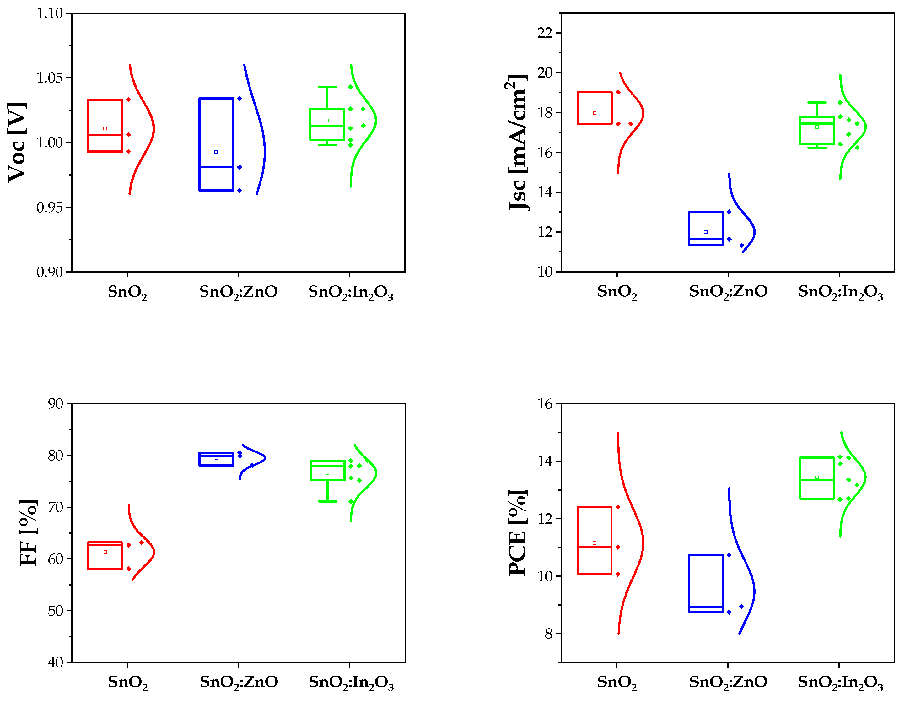
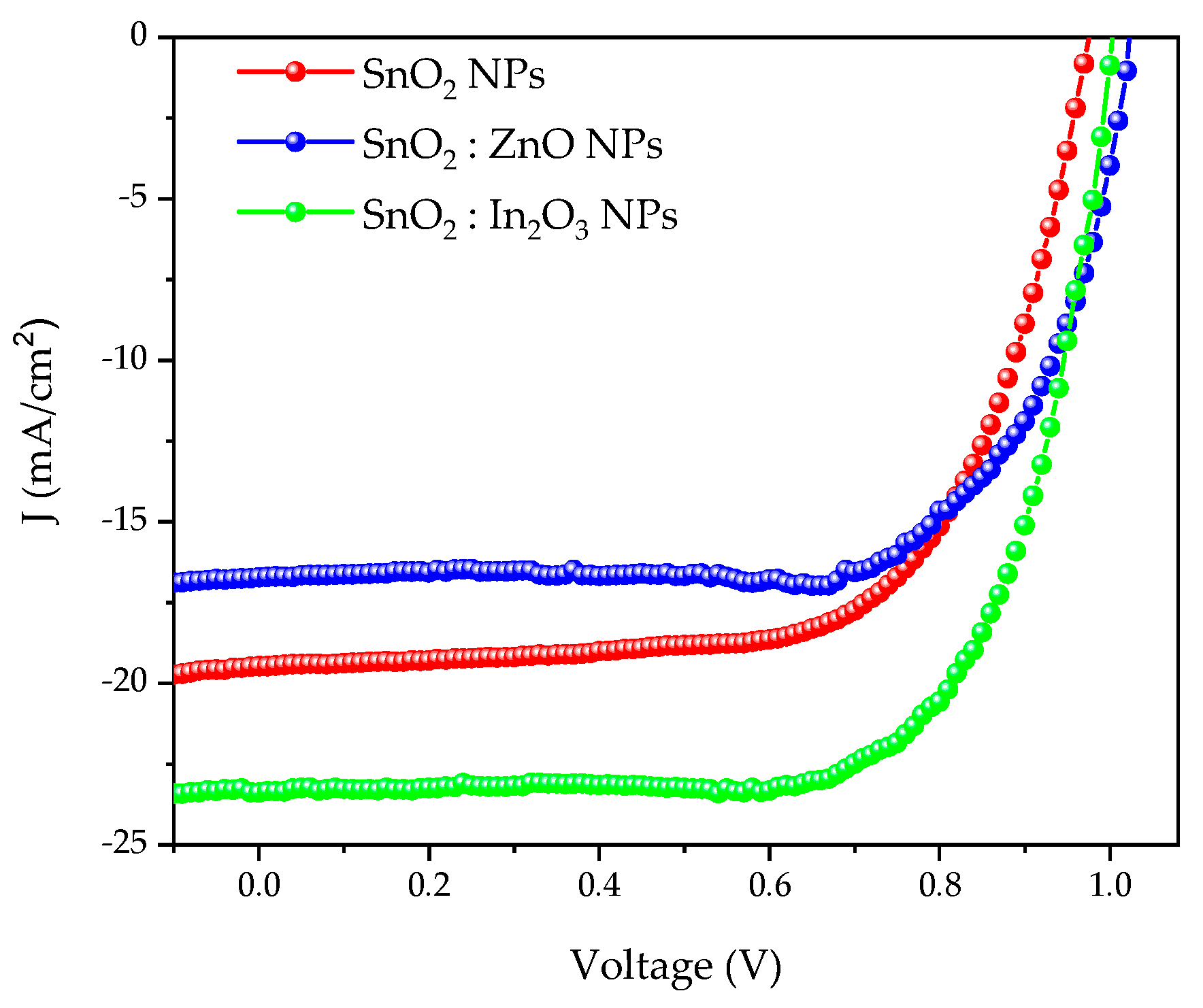
| ETL | Jsc [mA/cm2] | VOC [V] | FF [%] | PCE [%] |
|---|---|---|---|---|
| SnO2 | 18 1 | 1.01 0.02 | 61 3 | 11.2 1.2 |
| SnO2:ZnO SnO2:In2O3 | 12 1 17 1 | 0.99 0.04 1.02 0.02 | 79 1 73 3 | 9.5 1.1 13.4 0.6 |
| ETL | Jsc [mA/cm2] | VOC [V] | FF [%] | PCE [%] |
|---|---|---|---|---|
| SnO2 | 19.5 | 0.98 | 65.8 | 12.5 |
| SnO2:ZnO | 16.7 | 1.02 | 70.2 | 12.0 |
| SnO2:In2O3 | 23.3 | 1.00 | 70.3 | 16.4 |
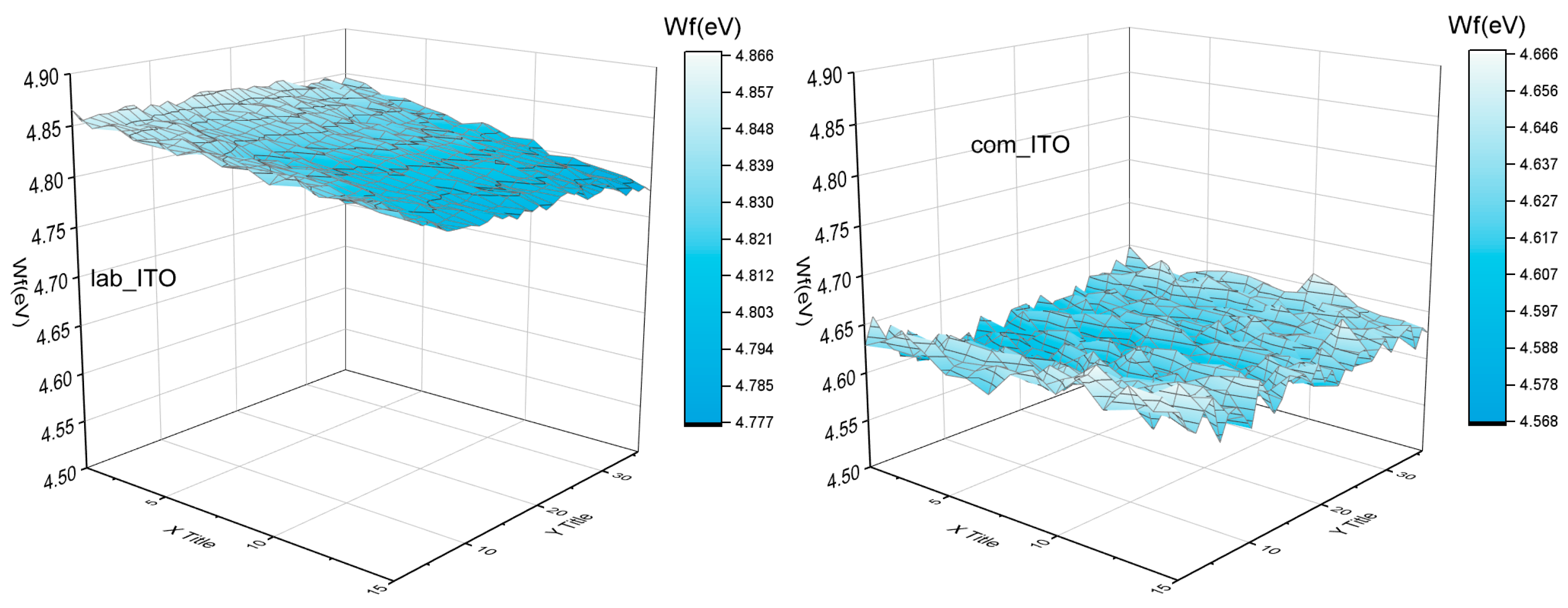
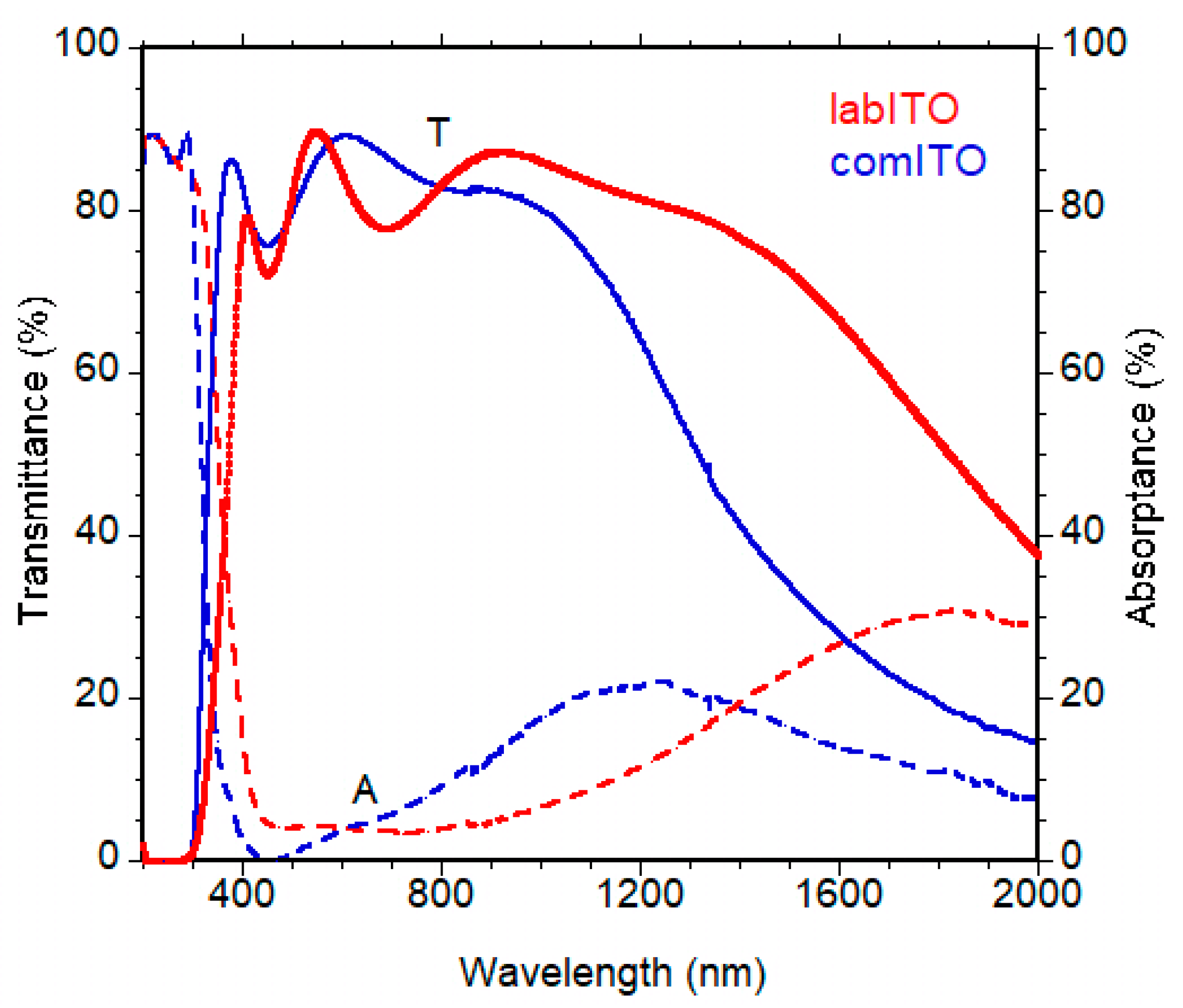
| TCO | Thickness [nm] | Rsh [ohm/sq] | ρ [Ω∗cm] × 10−4 | Ne [cm−3] × 1021 | Aav [%] | Eg [eV] |
|---|---|---|---|---|---|---|
| comITO | 180 | 10 | 1.8 | 1.2 | 8 | 3.83 |
| labITO | 285 | 11 | 3.2 | 0.55 | 9 | 3.65 |
Publisher’s Note: MDPI stays neutral with regard to jurisdictional claims in published maps and institutional affiliations. |
© 2021 by the authors. Licensee MDPI, Basel, Switzerland. This article is an open access article distributed under the terms and conditions of the Creative Commons Attribution (CC BY) license (https://creativecommons.org/licenses/by/4.0/).
Share and Cite
Sannino, G.V.; De Maria, A.; La Ferrara, V.; Rametta, G.; Mercaldo, L.V.; Addonizio, M.L.; Lancellotti, L.; Pecoraro, A.; Muñoz-García, A.B.; Pavone, M.; et al. Development of SnO2 Composites as Electron Transport Layer in Unencapsulated CH3NH3PbI3 Solar Cells. Solids 2021, 2, 407-419. https://doi.org/10.3390/solids2040026
Sannino GV, De Maria A, La Ferrara V, Rametta G, Mercaldo LV, Addonizio ML, Lancellotti L, Pecoraro A, Muñoz-García AB, Pavone M, et al. Development of SnO2 Composites as Electron Transport Layer in Unencapsulated CH3NH3PbI3 Solar Cells. Solids. 2021; 2(4):407-419. https://doi.org/10.3390/solids2040026
Chicago/Turabian StyleSannino, Gennaro V., Antonella De Maria, Vera La Ferrara, Gabriella Rametta, Lucia V. Mercaldo, Maria Luisa Addonizio, Laura Lancellotti, Adriana Pecoraro, Ana B. Muñoz-García, Michele Pavone, and et al. 2021. "Development of SnO2 Composites as Electron Transport Layer in Unencapsulated CH3NH3PbI3 Solar Cells" Solids 2, no. 4: 407-419. https://doi.org/10.3390/solids2040026
APA StyleSannino, G. V., De Maria, A., La Ferrara, V., Rametta, G., Mercaldo, L. V., Addonizio, M. L., Lancellotti, L., Pecoraro, A., Muñoz-García, A. B., Pavone, M., & Delli Veneri, P. (2021). Development of SnO2 Composites as Electron Transport Layer in Unencapsulated CH3NH3PbI3 Solar Cells. Solids, 2(4), 407-419. https://doi.org/10.3390/solids2040026