2.1. PV Modules and Arrays
Typically, PV panels comprise numerous interconnected PV cells, which are mechanically protected and suitable for sites with high solar radiation. Their principle of operation is based on the photoelectric effect, which explains that electrons are released when photons hit the PV panel.
Installing a single PV panel, such as for swimming pool heating, is sufficient in applications requiring only small amounts of energy. However, implementing PV arrays is necessary for more significant PV generation scenarios. In this case, PV panels are connected in series to achieve a greater voltage, in parallel to achieve a higher current, and in a mixed configuration to achieve higher power.
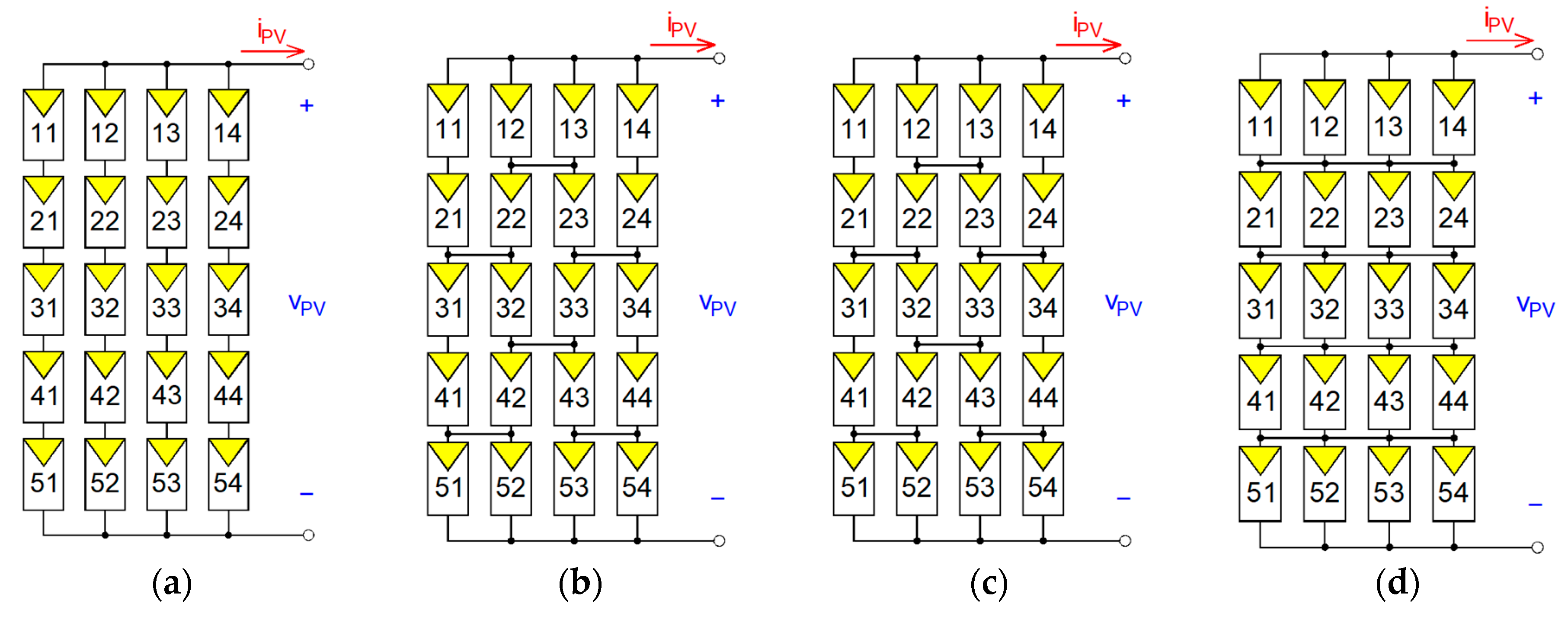
Figure 1 presents some connection topologies for a PV array, these being the Series–Parallel (SP), Bridge-linked (BL), Honeycomb (HC), and Total-Cross-Tied (TCT) [
15]. This paper considers the SP array. Its size depends on the maximum operating conditions of each connected PV panel and the manufacturer’s data.
Conventionally, these are operated at the maximum power point (MPP) to extract the maximum available PV power. The MPP depends on several conditions, such as the PV panels’ properties, climatic changes like light intensity decreasing due to the appearance of clouds, or unforeseen weather changes [
16]. MPP tracking can be implemented in the control circuit of the DC-DC converter to match the impedance of the PV array. This way, its operation can be stabilized at the maximum power point (MPP) or as close as possible to it. This power peak can be seen in
Figure 2 in the current/power characteristic curves of PV panels as a function of the voltage at their terminals. These characteristic curves indicate the MPP values for the PV arrays’ sizing. Their parameters are the
IMPP current and
PMPP power at a
VMPP voltage or remarkably close values [
17]. Additionally, the ranges of these curves are limited by the short-circuit current
ISC and the open-circuit voltage
VOC.
2.2. Boost Converter Design and Modeling
Power electronics-based energy conversion systems are used to optimize and efficiently use energy from PV systems. Since their output voltage is DC, a DC-DC converter such as the boost converter can be employed. When larger DC voltages are needed with lower input voltages and high efficiency, these converters are used in battery power applications, automotive applications, industrial drives, and adaptive control applications [
18].
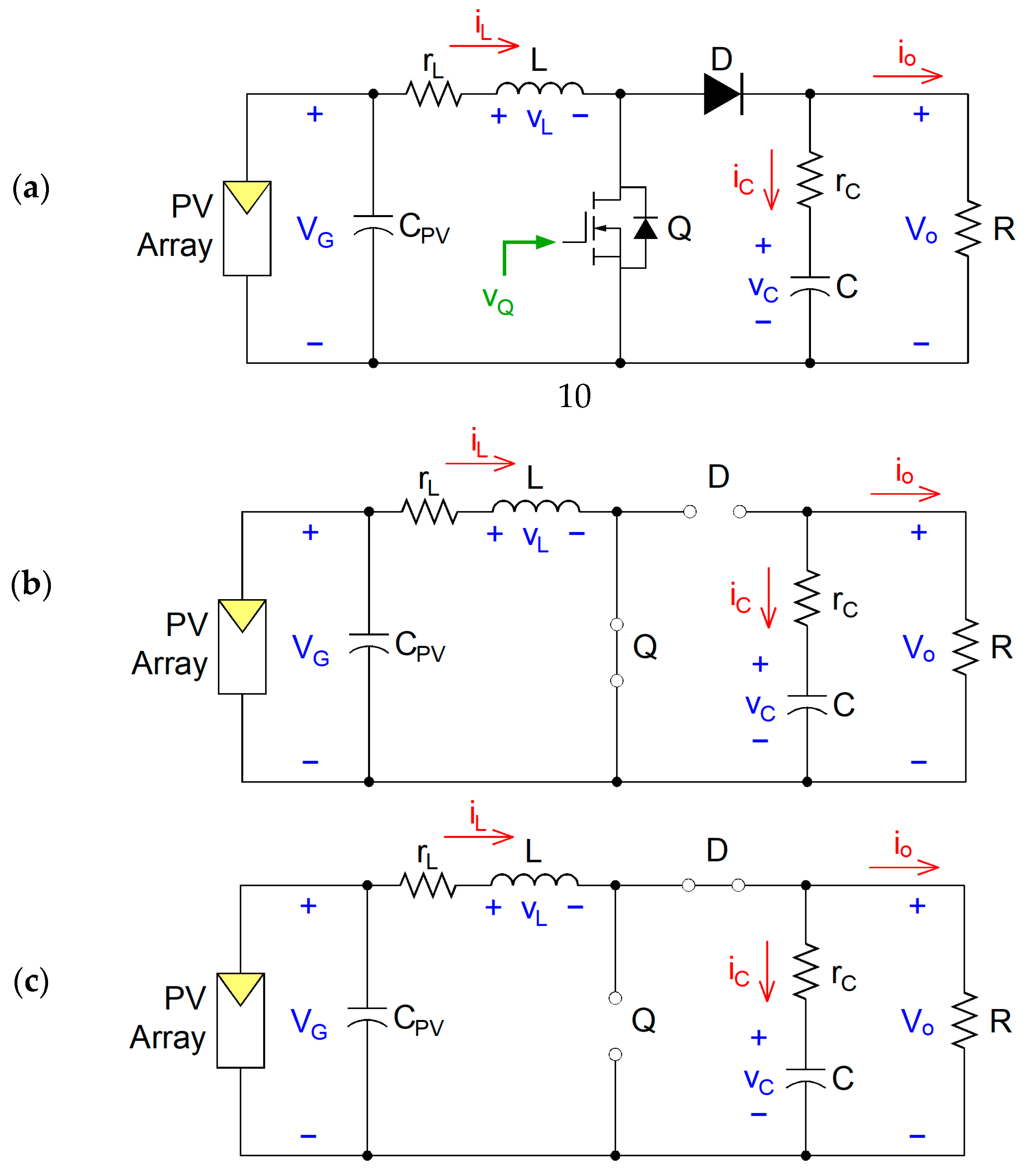
Figure 3a shows the power circuit of a boost converter, which is characterized by two operating states: In the “On-state”, shown in
Figure 3b, the
Q semiconductor acts as a switch, and when it is closed, an increase in the level of the inductor current
L is experienced. In contrast, the switch opens during the “Off-state” shown in
Figure 3c. The only possibility for inductor current to flow is through diode
D and the parallel configuration of output capacitor
C and load resistor
R. This leads to the capacitor transferring energy, which is acquired by it during the “On-state”. Additionally, the PV-generated power will oscillate due to a PV voltage ripple, resulting in a reduced average power output, and this is because of the installation of a
CPV capacitor for smoothing voltage ripples [
19].
Due to the operation of the semiconductor
Q, the output load voltage is chopped according to an operating duty cycle
D0 at a high switching frequency
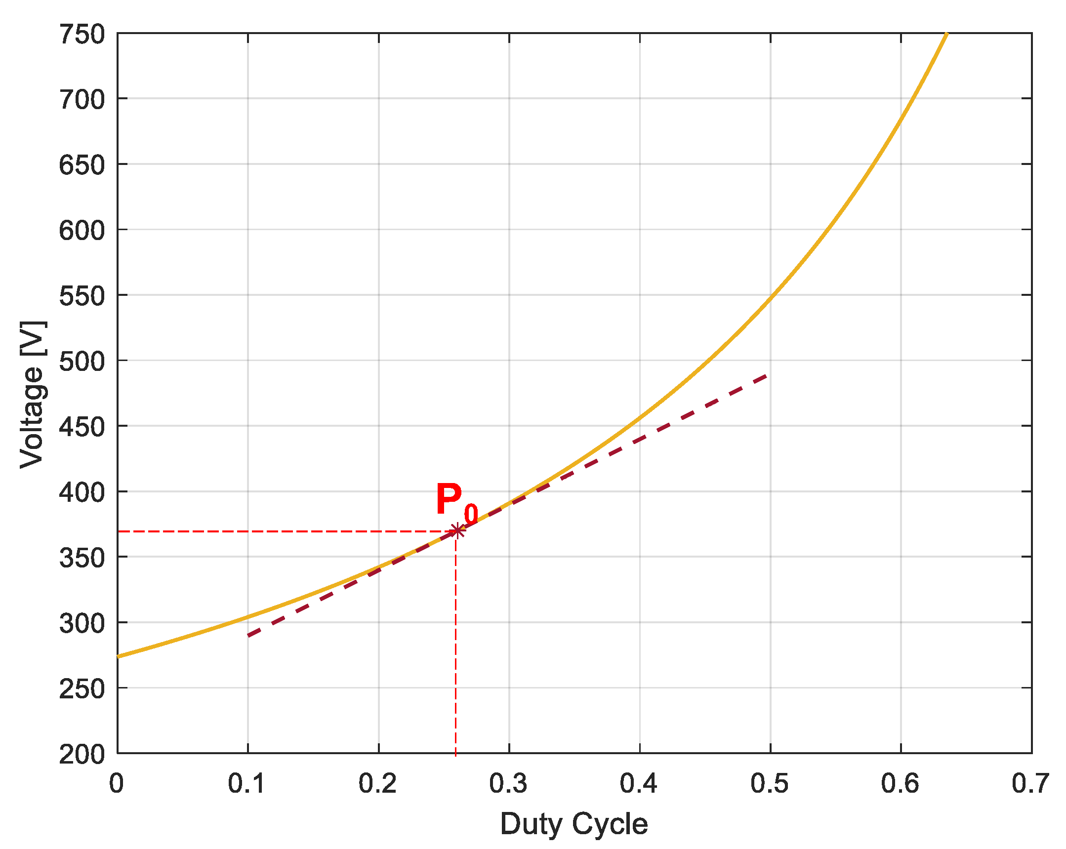
fSW and is calculated according to (1), where
VG is the PV voltage, and
V0 is the output voltage.
Continuous conduction mode (CCM) operation is desired in DC-DC switching converters. This means that the primary current, which is the inductor current in the converter, is not canceled out. The minimum values of its passive components R, L, and C together must be determined, along with its associated series resistances, considering primarily the power
Pn of the converter. In (2), the minimum inductance for the CCM current is determined according to [
20]. On the other hand, the minimum output capacitance can be determined by (3), according to [
20], where the output voltage ripple specification is usually between 1% and 5%.
Using a Schottky diode as a natural switching device and an IGBT as a forced switching device was considered to reduce power losses due to its higher current rating compared to a MOSFET.
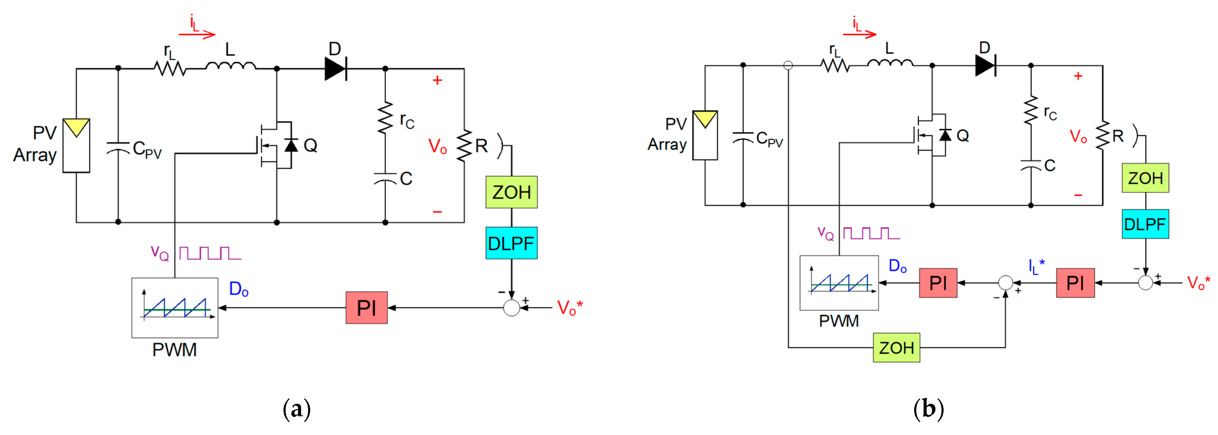
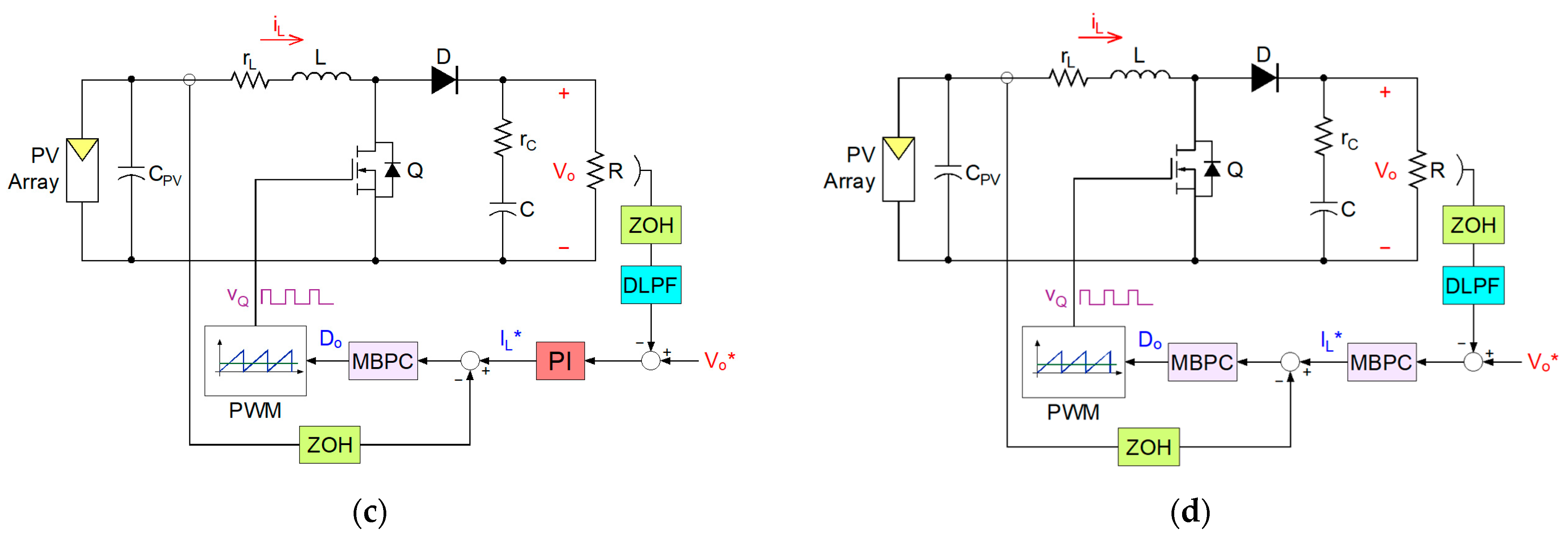
The principle of DC-DC converter control is PWM (Pulse Width Modulation), which is generated through the comparison of a constant modulating signal and a sawtooth carrier signal
vst at a switching frequency of
fSW [
21], or at a switching period of
TSW.
Figure 4 shows these waveforms together with their comparative results. Depending on whether the nominal duty cycle
D0 is increased or decreased, the resulting square signal pulse
vQ will either be broader or narrower at a constant frequency comparable to
fSW. It is important to note that the control signal
D0 will come from the implemented digital or predictive controller, and in some cases, it may come directly from an MPPT controller.
This technique has variations, such as the control signal being compared against an unbiased triangle wave instead of a sawtooth wave. Another novel method is establishing boundary voltages for the control signal, thus achieving an improved dynamic response [
22].
Once the parameters of the boost converter have been determined, the mathematical model of the system may be derived, with the averaged model state space matrixes Ap, Bp, Cp, and Dp, the state vector x = [iL vC]T, VG as an input, and V0 as an output. VG is considered only as an input because we aim to find the system dynamics only in the power stage. In this type of system, the input does not have a direct influence on the outputs, and for this reason, the Dp matrix is considered null.
Figure 3b shows the power circuit in the On-state [
13], where Kirchhoff’s current/voltage laws are applied in the first instance together with the laws of each energy storage component, thus obtaining (4) and (5):
Considering the output mesh:
With these expressions, the system behavior is obtained:
By applying a voltage divider on the output mesh, the output voltage in the On-state will be:
Similarly, the following expression in the first mesh for the boost converter in the Off-state [
13] will be:
The second mesh is analyzed as follows:
In this case, first, the output expression will be determined by replacing (11) in (10):
Considering (12) in the previous expressions, the following system behavior in a steady state is obtained:
Representation of the average model in steady space is performed for both switching periods. For
tON during a duty cycle
d and
tOFF during a complementary duty cycle 1
− d, the following average
Ap,
Bp, and
Cp matrixes are obtained:
With these matrixes, a system with two inputs,
u = [
d VG]
T, two states,
x = [
iL vC]
T, and one output,
V0, for the voltage regulation of the converter, as a function of slight duty cycle changes, is obtained.
