
Simple Chargers for a Small DC Micro-Grid for a Home Emergency Power System

Abstract
1. Introduction
2. Buck Battery Charger
2.1. Dimensioning
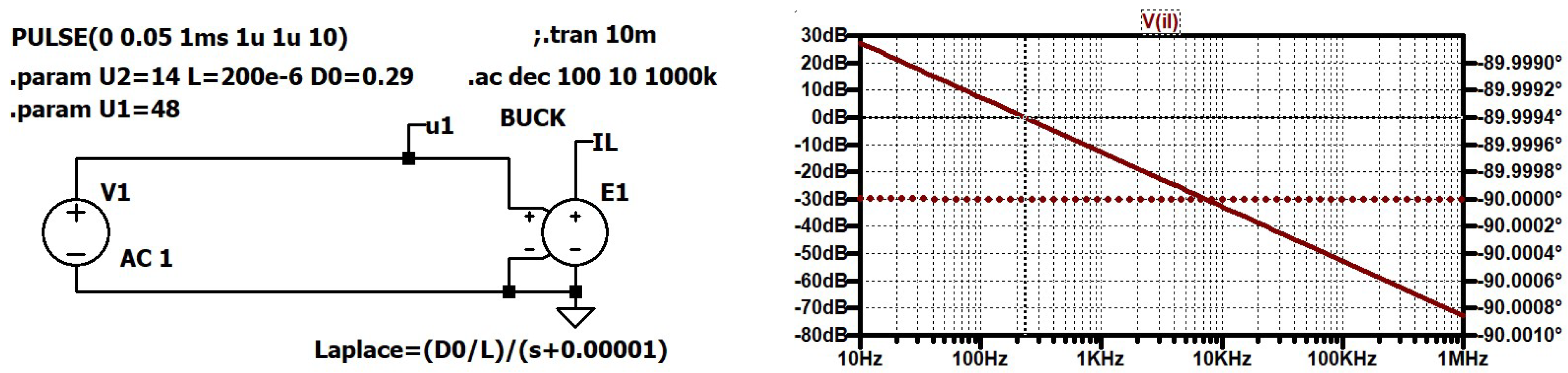
2.2. Model of the Buck Battery Charger
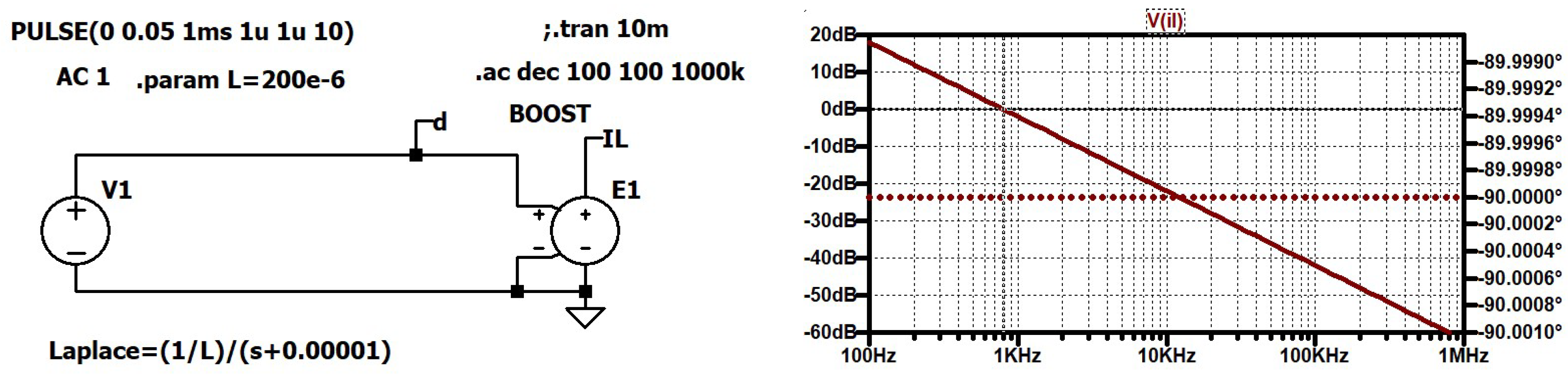
3. Simple Boost Battery Charger
3.1. Determination of the Desired Current Value
3.2. Design of the Inductor
3.3. Dynamics
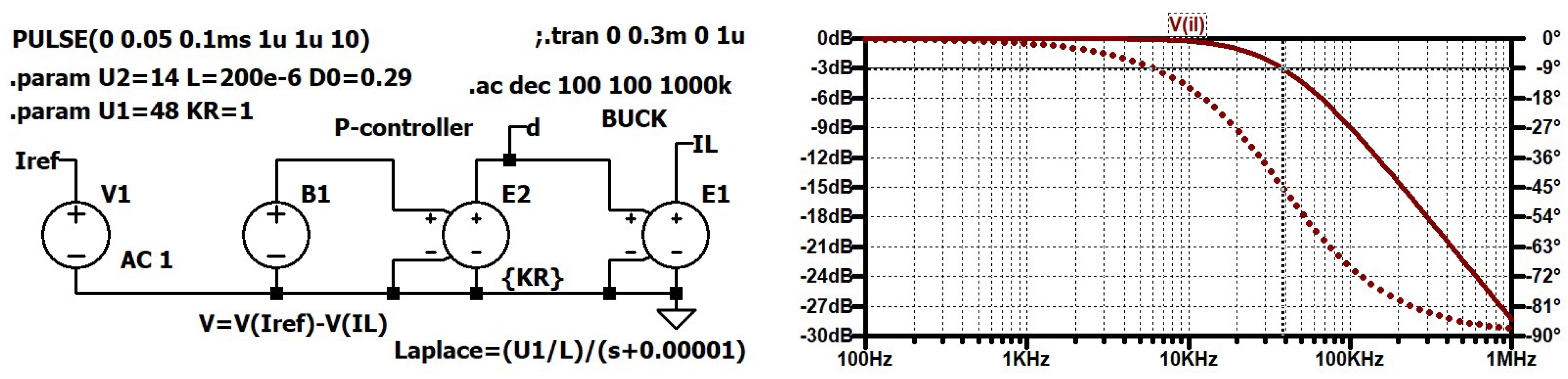
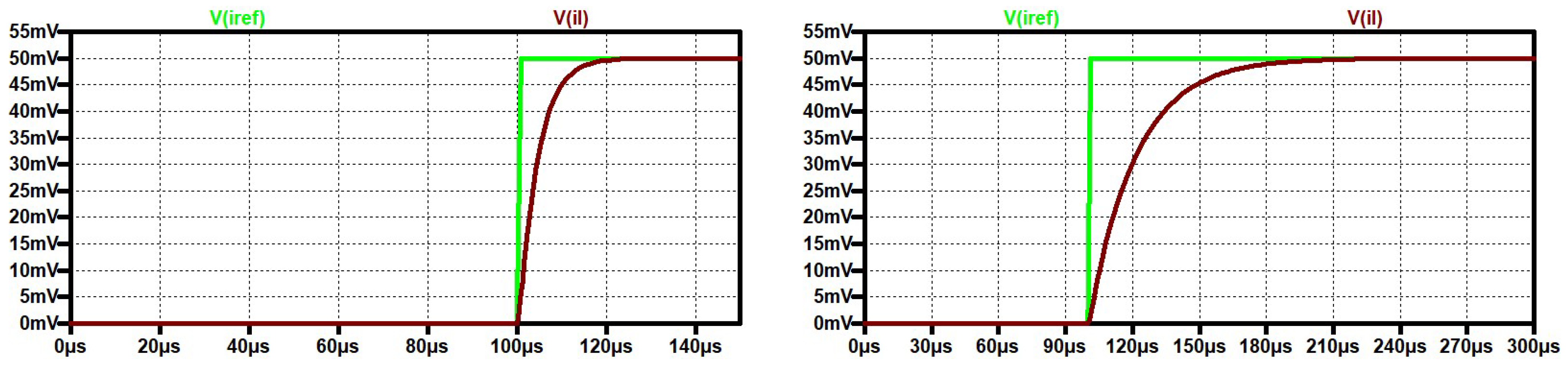
3.4. P-Controller
3.5. Hysteresis Controller
4. Conclusions
Author Contributions
Funding
Data Availability Statement
Acknowledgments
Conflicts of Interest
References
- Cecilia, A.; Sahoo, S.; Dragicevic, T.; Costa-Castello, R.; Blaabjerg, F. On Addressing the Security and Stability Issues Due to False Data Injection Attacks in DC Microgrids—An Adaptive Observer Approach. IEEE Trans. Power Electron. 2021, 37, 2801–2814. [Google Scholar] [CrossRef]
- Burgos-Mellado, C.; Donoso, F.; Dragicevic, T.; Cardenas-Dobson, R.; Wheeler, P.; Clare, J.C.; Watson, A.J. Cyber-Attacks in Modular Multilevel Converters. IEEE Trans. Power Electron. 2022, 37, 8488–8501. [Google Scholar] [CrossRef]
- Zhang, J.; Guo, L.; Ye, J. Cyber-attack Detection for Photovoltaic Farms based on Power-Electronics-Enabled Harmonic State Space Modeling. IEEE Trans. Smart Grid 2022, 13, 3929–3942. [Google Scholar] [CrossRef]
- Qiu, W.; Sun, K.; Li, K.-J.; Li, Y.; Duan, J.; Zhu, K. Cyber-Attack Detection: Modeling and Roof-PV Generation System Defending. IEEE Trans. Ind. Appl. 2023, 59, 160–168. [Google Scholar] [CrossRef]
- Chatterjee, A.; Paul, S.; Ganguly, B. Multi-Objective Energy Management of a Smart Home in Real Time Environment. IEEE Trans. Ind. Appl. 2023, 59, 138–147. [Google Scholar] [CrossRef]
- Anees, M.; Moaz, T.; Hussain, S.; Khan, H.A.; Nasir, M. Evaluation of System Losses for 48V and 380V Solar Powered LVDC Microgrids. In Proceedings of the 2020 IEEE Power & Energy Society General Meeting (PESGM), Montreal, QC, Canada, 2–6 August 2020; pp. 1–5. [Google Scholar] [CrossRef]
- Ambriz, O.; Onofre, L.; Hamlin, J.; Taufik, T.; Hasanah, R.N. Bi-Directional DC-DC Converter for the DC House Project. In Proceedings of the 2020 FORTEI-International Conference on Electrical Engineering (FORTEI-ICEE), Bandung, Indonesia, 23–24 September 2020; pp. 80–85. [Google Scholar] [CrossRef]
- Odo, P. Islanded dc Microgrid Design Using Non-Isolated Bidirectional Interleaved Half Bridge Converter for Energy Storage Application in a dc Microgrid. In Proceedings of the 2020 6th IEEE International Energy Conference (ENERGYCon), Gammarth, Tunisia, 28 September–1 October 2020; pp. 773–781. [Google Scholar] [CrossRef]
- Gospodinova, D.; Milanov, K.; Georgiev, M.; Dineff, P. Battery Choice According to Weather Conditions of a Hybrid System Designed for a Single-Family House in Bulgaria. In Proceedings of the 2021 13th Electrical Engineering Faculty Conference (BulEF), Varna, Bulgaria, 8–11 September 2021; pp. 1–5. [Google Scholar] [CrossRef]
- Moller, M.; Krauter, S. Model of an Automous PV Home using a Hybrid Storage System based on Li-ion batteries and Hydrogen Storage with Waste Heat Utilization. In Proceedings of the 2022 IEEE 49th Photovoltaics Specialists Conference (PVSC), Philadelphia, PA, USA, 5–10 June 2022; pp. 650–652. [Google Scholar] [CrossRef]
- Datasheet: AccuForce 12V-100Ah Lead Acid Battery (VRLA). Available online: https://energypower.gr/wp-content/uploads/2017/04/accuforce-12v-100ah.pdf (accessed on 25 March 2023).
- Alavi, S.M.M.; Mahdi, A.; Payne, S.J.; Howey, D.A. Identifiability of Generalized Randles Circuit Models. IEEE Trans. Control Syst. Technol. 2017, 25, 2112–2120. [Google Scholar] [CrossRef]
- Sihvo, J.; Stroe, D.-I.; Messo, T.; Roinila, T. Fast Approach for Battery Impedance Identification Using Pseudo-Random Sequence Signals. IEEE Trans. Power Electron. 2019, 35, 2548–2557. [Google Scholar] [CrossRef]
- Zhu, J.; Sun, Z.; Wei, X.; Dai, H. Studies on the medium-frequency impedance arc for Lithium-ion batteries considering various alternating current amplitudes. J. Appl. Electrochem. 2015, 46, 157–167. [Google Scholar] [CrossRef]
- Wu, S.-L.; Chen, H.-C.; Chou, S.-R. Fast Estimation of State of Charge for Lithium-Ion Batteries. Energies 2014, 7, 3438–3452. [Google Scholar] [CrossRef]
- Mohan, N.; Undeland, T.; Robbins, W. Power Electronics, Converters, Applications and Design, 3rd ed.; John Wiley & Sons: New York, NY, USA, 2003. [Google Scholar]
- Zach, F. Power Electronics, in German: Leistungselektronik, 6th ed.; Springer: Frankfurt, Germany, 2022. [Google Scholar]
- Rozanov, Y.; Ryvkin, S.; Chaplygin, E.; Voronin, P. Power Electronics Basics; CRC Press: Boca Raton, FL, USA, 2016. [Google Scholar]
- Bosnjic, Z.; Krischan, K. Single-phase grid interface for home energy storage. Elektrotech. Inftech. 2023, 140, 103–109. [Google Scholar] [CrossRef]
- Heydari-Doostabad, H.; Hosseini, S.H.; Ghazi, R.; O’Donnell, T. Pseudo DC-Link EV Home Charger With a High Semiconductor Device Utilization Factor. IEEE Trans. Ind. Electron. 2021, 69, 2459–2469. [Google Scholar] [CrossRef]
- Kudryavtsev, A.; Zatsepina, V. Laboratory Installation to Demonstrate the Advantages of a DC Network in a Smart Home. In Proceedings of the 2022 2nd International Conference on Technology Enhanced Learning in Higher Education (TELE), Lipetsk, Russia, 26–27 May 2022; pp. 105–108. [Google Scholar] [CrossRef]
- Carvalho, E.L.; Blinov, A.; Chub, A.; Vinnikov, D. Overview of Single-Stage Isolated AC-DC Topologies for Interfacing DC and AC Grids. In Proceedings of the 2022 IEEE 13th International Symposium on Power Electronics for Distributed Generation Systems (PEDG), Kiel, Germany, 26–29 June 2022; pp. 1–6. [Google Scholar] [CrossRef]
- Carvalho, E.L.; Blinov, A.; Chub, A.; Vinnikov, D. Analysis of Holdup Time for DC Grid-Forming Isolated Active Front-End Converters. In Proceedings of the IECON 2022–48th Annual Conference of the IEEE Industrial Electronics Society, Brussels, Belgium, 17–20 October 2022; pp. 1–6. [Google Scholar] [CrossRef]
- Sunny, A.C.; Surulivel, N.; Debnath, D. Solar-Battery-Integrated Hybrid AC/DC Off-Grid System for Rural Households Based on a Novel Multioutput Converter. IEEE J. Emerg. Sel. Top. Power Electron. 2022, 10, 6208–6217. [Google Scholar] [CrossRef]
- Manas, K.; Gupta, J.; Singh, B. Roof Top Solar PV Supported Electric Vehicle Charging System for Home Parking Spaces. In Proceedings of the 2022 IEEE Industry Applications Society Annual Meeting (IAS), Detroit, MI, USA, 9–13 October 2022; pp. 1–6. [Google Scholar] [CrossRef]
- Zhao, D.; Jiang, S.; Hu, D.; Wang, Y.; Jin, X.; Sun, C. Summary and Prospect of Technology Development of MVDC and LVDC Distribution Technology. In Proceedings of the 2022 IEEE 5th International Electrical and Energy Conference (CIEEC), Nangjing, China, 27–29 May 2022; pp. 1294–1300. [Google Scholar] [CrossRef]
- Kaushik, H.; Bhushan, B. Performance Analysis of Boost Converters in a PV System with P and O based MPPT Controller connected to a Battery Backup and Grid. In Proceedings of the 2022 IEEE Delhi Section Conference (DELCON), New Delhi, India, 11–13 February 2022; pp. 1–7. [Google Scholar] [CrossRef]
- Li, L.; Li, K.-J.; Sun, K.; Liu, Z.; Lee, W.-J. A Comparative Study on Voltage Level Standard for DC Residential Power Systems. IEEE Trans. Ind. Appl. 2022, 58, 1446–1455. [Google Scholar] [CrossRef]
- Tyagi, S.; Singh, B. A Solar PV-Small Hydro Energy Conversion System Powered Charging Infrastructure. In Proceedings of the 2022 IEEE IAS Global Conference on Emerging Technologies (GlobConET), Arad, Romania, 20–22 May 2022; pp. 503–508. [Google Scholar] [CrossRef]
- Himmelstoss, F.A. Design of State-Space Controllers with the Help of Signal Flow Graphs Shown for a Buck Converter. WSEAS Trans. Syst. 2022, 21, 421–429. [Google Scholar] [CrossRef]


Disclaimer/Publisher’s Note: The statements, opinions and data contained in all publications are solely those of the individual author(s) and contributor(s) and not of MDPI and/or the editor(s). MDPI and/or the editor(s) disclaim responsibility for any injury to people or property resulting from any ideas, methods, instructions or products referred to in the content. |
© 2023 by the authors. Licensee MDPI, Basel, Switzerland. This article is an open access article distributed under the terms and conditions of the Creative Commons Attribution (CC BY) license (https://creativecommons.org/licenses/by/4.0/).
Share and Cite
Himmelstoss, F.A.; Votzi, H.L. Simple Chargers for a Small DC Micro-Grid for a Home Emergency Power System. Electricity 2023, 4, 216-234. https://doi.org/10.3390/electricity4030013
Himmelstoss FA, Votzi HL. Simple Chargers for a Small DC Micro-Grid for a Home Emergency Power System. Electricity. 2023; 4(3):216-234. https://doi.org/10.3390/electricity4030013
Chicago/Turabian StyleHimmelstoss, Felix A., and Helmut L. Votzi. 2023. "Simple Chargers for a Small DC Micro-Grid for a Home Emergency Power System" Electricity 4, no. 3: 216-234. https://doi.org/10.3390/electricity4030013
APA StyleHimmelstoss, F. A., & Votzi, H. L. (2023). Simple Chargers for a Small DC Micro-Grid for a Home Emergency Power System. Electricity, 4(3), 216-234. https://doi.org/10.3390/electricity4030013