Proceeding Paper

Application of Artificial Intelligence to Improve Chip Defect Detection Using Semiconductor Equipment †

Department of Business Administration, Chaoyang University of Technology, Taichung 411310, Taiwan
*
Author to whom correspondence should be addressed.
Presented at the 2024 4th International Conference on Social Sciences and Intelligence Management (SSIM 2024), Taichung, Taiwan, 20–22 December 2024.
Eng. Proc. 2025, 98(1), 26; https://doi.org/10.3390/engproc2025098026
Published: 30 June 2025

Abstract

We investigated the application of artificial intelligence (AI) technology for the inspection of semiconductor process equipment to address key issues such as low production efficiency and high equipment failure rates. The semiconductor industry, being central to modern technology, requires complex and precise processes where even minor defects lead to product failures, negatively impacting yield and increasing costs. Traditional inspection methods are not adequate for modern high-precision, high-efficiency production demands. By integrating advanced AI technologies, such as machine learning, deep learning, and pattern recognition, large volumes of experimental data are collected and analyzed to optimize process parameters, enhance stability, and improve product yield. By using AI, the identification and classification of defects are automated to predict potential equipment failures and reduce downtime and overall costs. By combining AI with automated optical inspection (AOI) systems, a widely used defect detection tool has been developed for semiconductor manufacturing. However, under complex conditions, AOI systems are prone to producing false positives, resulting in overkill rates above 20%. This wastes perfect products and increases the cost due to the need for manual re-inspection, hindering production efficiency. This study aims to improve wafer inspection accuracy using AI technology and reduce false alarms and overkill rates. By developing intelligent detection models, the system automatically filters out false defects and minimizes manual intervention, boosting inspection efficiency. We explored how AI is used to analyze inspection data to identify process issues and optimize workflows. The results contribute to the reduction in labor and time costs, improving equipment performance, and significantly benefitting semiconductor production management. The AI-driven method can be applied to other manufacturing processes to enhance efficiency and product quality and support the sustainable growth of the semiconductor industry.

1. Introduction

As semiconductor technology enters nanoscale manufacturing, process control and quality management become more difficult. Even small defects cause entire batches of products to be scrapped, leading to huge economic losses. Traditional automatic optical inspection (AOI) is prone to misjudgment in a complex process. Especially when detecting highly reflective materials and complex patterns, the error rate reaches higher than 20%, increasing manpower and re-inspection costs. To solve this problem, artificial intelligence (AI) technology is introduced in semiconductor inspection, and process parameters are optimized by machine learning, deep learning, and pattern recognition to improve stability and yield.
AI technology is used for intelligent monitoring and establishing prediction models to reduce downtime and production costs. A large amount of experimental data, including normal and defect sample image data, is necessary to train an AI model and improve the generalization ability of the model through data enhancement and feature extraction.
Research is mandated to effectively integrate AI models into existing AOI systems to improve detection accuracy and speed through hardware acceleration, software optimization, and human–machine interface design. The results contribute to significantly reducing overkill and misjudgment rates, improving yield, and reducing material waste and production costs. Detection efficiency and automation levels can be enhanced, reducing labor costs.
AI’s intelligent monitoring and prediction functions are essential for preventive maintenance and decreasing downtime and maintenance costs. Technology that combines AI and AOI improves corporate production efficiency and competitiveness in the fierce global competitive environment. The technology can also be applied to other high-precision manufacturing sectors, such as advanced semiconductor, biomedicine, and aerospace manufacturing. This technology provides additional technological innovation.

2. Literature Review

2.1. Traditional AOI Technology

As processes advance, AOI encounters challenges in identifying small defects. Especially in wafer packaging, 3D technologies are used for micro-bumping, redistribution, ball attach, chip-to-wafer (C2W), wafer-to-wafer (W2W), deboning, and TSV technology. More innovations in advanced packaging technology and more complex integration are required to decrease false positive rates [1]. Defects in the integrated circuit (IC) manufacturing and packaging processes are prevented by inspecting wafer quality [2].
It is difficult to accurately identify various types of defects when using traditional AOI technology. For example, tiny particles or slight scratches increase the overkill rate, which requires eliminating finished products. Traditional AOI image analysis technology faces challenges in accurately identifying such defects [3].

2.2. AI Technology

AI technology, especially machine learning and deep learning, has been used for defect identification and classification. AI technology automatically classifies defects into different types based on their characteristics, such as scratches, dents, foreign matter, or contamination [4]. The difference between machine learning and deep learning lies in the way data is processed. For example, color, shape, and texture are learned and classified using deep learning algorithms that automatically learn features from data and process complex images [5]. AI technology is used to predict the occurrence probability and trend of defects by analyzing process parameters, environmental data, and equipment status to take preventive measures to avoid the occurrence of defects [6].
AI technology has changed the semiconductor inspection process. It improves the yield of products and effectively reduces production costs [5]. The AI process presently plays an essential role in the inspection process [7,8,9].

2.2.1. Machine Learning in Defect Detection

Early research focused on traditional machine learning algorithms, support vector machine (SVM), and random forest (KNN) to classify defects [5]. These methods require manual feature extraction and classification. In contrast, machine learning algorithms analyze large amounts of data, extract characteristics of defects, build predictive models, and effectively identify defects that are difficult to detect using previous methods [10].

2.2.2. AI and AOI

AI technology embedded in an AOI system conducts intelligent image analysis using deep learning models. These models automatically learn and analyze defect features in complex images, overcoming the limitations of traditional AOI relying on manually set rules. This automated analysis considerably improves detection accuracy [4,11].
In semiconductor manufacturing, wafer testing is performed to ensure the performance of each wafer. The wafer map is used to visualize the color-coded wafer test results based on the locations. The defects on the wafer map are randomly distributed or form clustered patterns. The various clustered defect patterns are caused by assignable faults. The identification of the patterns is important to provide data on the root causes of diagnosis. By solving the problems, the manufacturing processes are improved, and costs are reduced. In this study, we present a novel convolutional neural network (CNN)-based method to automatically recognize the defect pattern on wafer maps. The developed method in this study adopts polar mapping before the training of the CNN to transform the circular wafer map into a matrix that is processed in the CNN architecture. The method reduces the input size and solves variations in wafer and die sizes. To eliminate the need for rotation, we apply data augmentation in training the CNN. Experiments using the real-world dataset prove the effectiveness and superiority of our method [12].
AI technology has a large potential in the semiconductor industry based on its functions and the characteristics of existing equipment. High precision, high positioning accuracy, rapid detection, and effective management are advantages of the developed method, which lead to improved product yield and corporate competitiveness. The current status and limits of existing methods are explored with their challenges and deficiencies. The test results provide a reference for further research [13].

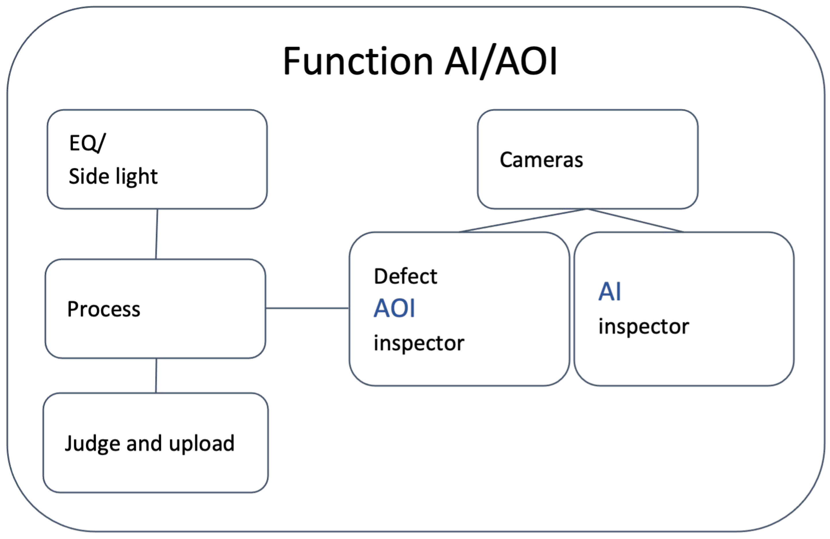
3. Research Methodology

We adopted a deductive method through a literature review. Three hypotheses were proposed and tested using algorithms and model architectures.
  • H1: By utilizing advanced algorithms such as CNN in deep learning, the accuracy of AOI systems is improved in identifying chip defects, thereby reducing the overkill rate.
  • H2: By precisely setting detection parameters and combining the learning capabilities of AI models, the system adapts to different environmental changes, reducing misjudgments caused by environmental factors.
  • H3: Introducing AI technology into AOI systems shortens the inspection time and reduces the need for manual re-inspection, thereby lowering costs and enhancing manufacturing efficiency.
In the training phase, the AI system learns how to identify qualified products. A small number of confirmed “OK samples” are uploaded to the AI computer as initial training data. AI learns the standard features of products and establishes basic recognition capabilities. The AI system continuously learns new data to improve detection accuracy. This re-learning mechanism makes AI smarter and more accurate in processing data in different situations. The precision detection capabilities of traditional AOI technology are integrated with the advantages of AI, improving the efficiency, accuracy, and automation of production line detection (Figure 1).
To adjust the angle of the light source, different textures and features of the object surface must be learned. Side light is used to highlight surface texture, while front light is used to highlight the shape of the object. By adjusting the angle of the light sources, glare caused by high angles and shadows caused by low angles are removed to obtain more accurate images and improve detection accuracy. AI technology is also used to optimize light source settings to reduce the overkill rate of the AOI system, improve detection accuracy and efficiency, and benefit the manufacturing industry.
In the process, AI technology effectively reduces the overkill rate of the AOI system, improves the yield rate of chip inspection, reduces labor and time costs, and improves manufacturing efficiency. Advanced algorithms such as CNN in deep learning improve the accuracy of the AOI system in identifying wafer defects, thereby reducing the overkill rate. When there are 200 no-good (NG) chips with a known overkill rate, the first overkill rate can be 27 chips, which is reduced to 13 chips using AI technology.

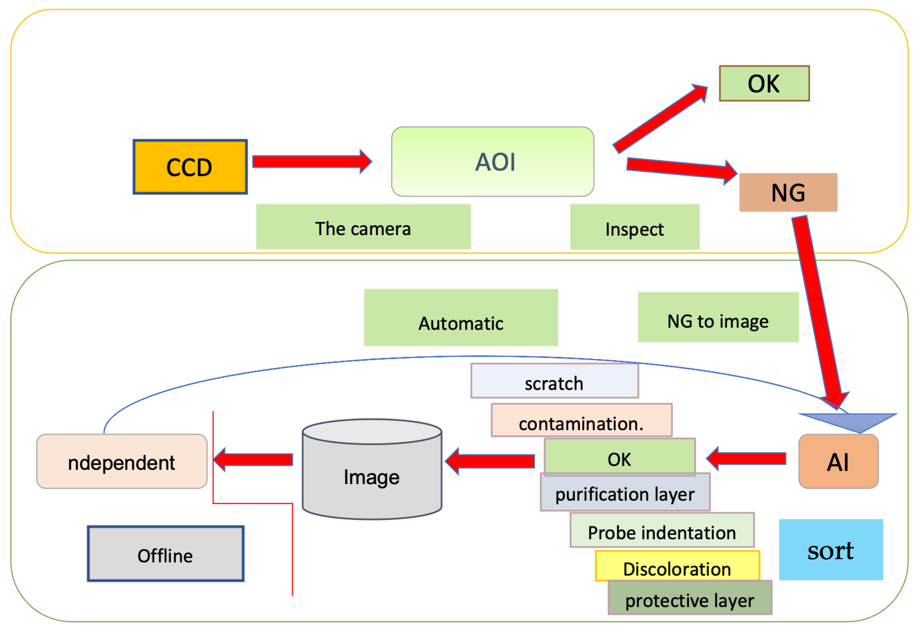
3.1. CNN in AOI System

CNN is a deep learning model particularly appropriate for image recognition and classification. In the AOI system, CNN automatically learns the features in the wafer image to identify subtle defects and detect different defects, thereby improving the accuracy of detection and reducing the overkill rate (Figure 2). Table 1 illustrates an example of reducing the overkill rate. In the initial condition, the number of NG wafers with an overkill rate is 200. The traditional AOI system is not able to accurately distinguish between real defects and normal variations, resulting in a high overkill rate.

3.2. Reducing Defective Rate

To improve the accuracy of chip inspection, the CNN model needs to be optimized. First, it is necessary to collect more wafer images of different situations which include various defects and normal samples to increase the amount and diversity of data. At the same time, data enhancement is performed, such as rotation, scaling, and adding noise to improve the generalization ability of the model. In application, the detection accuracy of the AOI system has been greatly improved with CNN. From the initial 200 overkill NG chips, after optimizing the AI algorithm, the overkill rate is reduced to 27 in the first inspection. After further optimization of the AI response system, the overkill rate is reduced to 13.
Such an improvement is attributed to continuous model optimization and learning to continuously improve detection accuracy and the improved performance of the detection system through optimizing models, improving the environment, and human–machine collaboration. As a result, product yield is increased by reducing the number of qualified products being misjudged as defective products, and production efficiency is enhanced. By reducing material waste and manual re-inspection costs, overall efficiency is increased. In addition, the improvement of product quality enhances the competitiveness of the company as the high standards of the market and customers are satisfied.

4. Results

The first misjudgment rate was 13.5%, so the AI algorithm repeated the process to reduce the overkill rate. The misjudgment rates in the first and second detections were calculated again. The misjudgment rate dropped significantly, which reflected the importance of continuous optimization of the model (Table 2).

4.1. First Test Results

In the first test, 200 defects were randomly detected from the NG box for testing and analysis. First, the total sample number (N) was 200 pieces. The number of defective products (real NG) was assumed to be 30, while the number of good products was 170 (Table 3 and Table 4).
  • F a l s e   p o s i t i v e   r a t e F P = F P N = 13.5 %
  • FP = False Positive rate × Total sample size = 13.5% × 200 = 27 units.
The first detection results are presented in Table 4.
  • A c c u r a c y = T P + T N N = 30 + 143 200 = 86.5%
  • p r e c i s i o n = T P T P + F P = 30 30 + 27 = 52.63%
  • Recall = T P T P + F N = 30 30 + 27 = 100 %
  • F1Score = 2 P r e c i s i o n R e c a l l P r e c i s i o n + R e c a l l = 0.6897%

4.2. Second Detection Result

With the AI algorithm, 200 pieces were randomly selected from the NG box for inspection. The false positive rate dropped to 6% ( F P = F P N = 6 % ). The number of false positives was as follows: FP = 6% × 200 = 12 pieces. The second detection results are presented in Table 5.
  • A c c u r a c y = T P + T N N = 30 + 158 200 = 94 %
  • p r e c i s i o n = T P T P + F P = 30 30 + 12 = 71.43 %
  • Recall = T P T P + F N = 30 30 + 0 = 100 %
  • F1Score = 2 P r e c i s i o n R e c a l l P r e c i s i o n + R e c a l l = 0.8333%

4.3. Comparison of Results

The “false positive rate”, “accuracy rate”, “precision rate”, “recall rate”, and “F1 score” of the tests were compared, as shown in Table 6.
The false positive rate is calculated as F P R = F P F P + T N × 100 % . In the first test, F P R = 27 27 + 143 × 100 %   = 15.88%, while in the second test, F P R = 12 12 + 158 × 100 %   = 7.06%. The false negative rate is calculated as F N R = T N T N F P × 100 % . The average F N R   = 0 0 + 30 × 100 % = 0 % .
The specificity is calculated as S p e c i f i c i t y = F N F N + T P × 100 % . In the first test, S p e c i f i c i t y = 143 143 + 27 × 100 % = 84.11%, while in the second test, S p e c i f i c i t y = 158 158 + 12 × 100 % = 92.94%.

5. Conclusions

After the optimization of the AI algorithm, the overall detection accuracy was significantly improved. First of all, the misidentification rate dropped from 13.5 to 6%, indicating that the number of misidentifications decreased by 55.6%, from 27 to 12. The detection accuracy increased from 86.5 to 94%, indicating that the correctness of the system was significantly improved. The accuracy increased from 52.63 to 71.43%. This showed that the proportion of actual defective products increased, significantly reducing the misidentification of good products. At the same time, the recall rate was maintained at 100%, indicating that all defective products were detected without any misjudgments. In addition, the F1 score increased from approximately 0.6897 to 0.8333, showing a significant improvement in the overall performance of the model.
The effectiveness of AI technology has been proven in the test. The model’s ability to distinguish good products from defective products has been significantly improved. In particular, the identification of good products became more accurate with reduced overkill rates. The reduction in misjudgment rates improved production efficiency and reduced unnecessary work and manpower for re-inspection. Time and costs were saved, improving production efficiency. In addition, the training process enhanced the criticality of data quality and diversity. By learning more diverse samples, the model’s recognition ability can be enhanced to detect different types of defects.
Future improvement is still needed to detect new types of defects during the production process. Increasing the sample size is an important strategy for collecting and annotating more defect samples that are difficult to distinguish at present. The learning effect of the model can be much improved by applying more advanced deep learning models, allowing AI systems to be more effective in production environments. The overkill rate and detection accuracy are significantly improved, which helps to increase product yield and reduce production costs. Therefore, the competitiveness of companies can be enhanced by continuously optimizing the model and increasing the amount of data.

Author Contributions

Conceptualization, C.-J.F. and H.-Y.T.; Methodology, H.-Y.T.; Formal Analysis, H.-Y.T.; Investigation, H.-L.C.; Resources, H.-L.C.; Data Curation, H.-Y.T.; Writing—Original Draft, H.-Y.T.; Supervision, C.-J.F.; Project Administrator, H.-Y.T. All authors have read and agreed to the published version of the manuscript.

Funding

This research received no external funding.

Institutional Review Board Statement

Not applicable.

Informed Consent Statement

Not applicable.

Data Availability Statement

The information utilized to substantiate the outcomes of this research can be obtained by contacting the corresponding author via email at yenco@msm.com.tw.

Conflicts of Interest

The authors declare no conflicts of interest.

References

  1. Chen, J.; Li, X.; Wang, Y. Challenges of AOI in advanced semiconductor manufacturing. Semicond. Manuf. Technol. 2018, 25, 45–52. [Google Scholar]
  2. Chen, M.F.; Chou, C.C.; Lien, C.C.; Weng, R.C. Development of an AOI system for chips with a hole on backside based on a frame imager. In Proceedings of the Seventh International Symposium on Precision Mechanical Measurements, Xiamen, China, 7–12 August 2015; SPIE: Bellingham, WA, USA, 2016; Volume 9903, pp. 376–381. [Google Scholar]
  3. Li, X.; Dong, Y.; Yang, F. Automated defect detection with deep learning in AOI systems. J. Intell. Manuf. 2021, 32, 2053–2065. [Google Scholar]
  4. Hou, Z. Research on adopting artificial intelligence technology to improve effectiveness of vocational college English learning. J. Phys. Conf. Ser. 2021, 1744, 042122. [Google Scholar] [CrossRef]
  5. Mezher, A.M.; Marble, A.E. A novel strategy for improving robustness in computer vision manufacturing defect detection. arXiv 2023, arXiv:2305.09407. [Google Scholar] [CrossRef]
  6. Zhang, W. Penelitian Tentang Algoritma Diagnosis Kesalahan Bantalan Berdasarkan Jaringan Saraf Konvolusional. Doctoral Dissertation, Harbin Institute of Technology, Harbin, China, 2017. [Google Scholar]
  7. Abd Al Rahman, M.; Mousavi, A. A review and analysis of automatic optical inspection and quality monitoring methods in electronics industry. IEEE Access 2020, 8, 183192–183271. [Google Scholar]
  8. Chouchene, A.; Carvalho, A.; Lima, T.M.; Charrua-Santos, F.; Osório, G.J.; Barhoumi, W. Artificial intelligence for product quality inspection toward smart industries: Quality control of vehicle non-conformities. In Proceedings of the 2020 9th International Conference on Industrial Technology and Management (ICITM), Oxford, UK, 11–13 February 2020; IEEE: Piscataway, NJ, USA, 2020; pp. 127–131. [Google Scholar] [CrossRef]
  9. Ding, H.; Gao, R.X.; Isaksson, A.J.; Landers, R.G.; Parisini, T.; Yuan, Y. State of AI-based monitoring in smart manufacturing and introduction to focused section. IEEE/ASME Trans. Mechatron. 2020, 25, 2143–2154. [Google Scholar] [CrossRef]
  10. Wang, H.; Zhang, L.; Li, Y. Deep learning for defect detection in manufacturing: Advantages over traditional methods. IEEE Trans. Ind. Electron. 2021, 68, 7564–7572. [Google Scholar]
  11. Chen, Y.; Ding, Y.; Zhao, F.; Zhang, E.; Wu, Z.; Shao, L. Surface defect detection methods for industrial products: A review. Appl. Sci. 2021, 11, 7657. [Google Scholar] [CrossRef]
  12. Wang, R.; Chen, N. Defect pattern recognition on wafers using convolutional neural networks. Qual. Reliab. Eng. Int. 2020, 36, 1245–1257. [Google Scholar] [CrossRef]
  13. Yang, J.; Li, S.; Wang, Z.; Dong, H.; Wang, J.; Tang, S. Using deep learning to detect defects in manufacturing: A comprehensive survey and current challenges. Materials 2020, 13, 5755. [Google Scholar] [CrossRef] [PubMed]
Figure 1. Operation of AI-integrated AOI.
Engproc 98 00026 g001
Figure 2. Defect classification process.
Engproc 98 00026 g002
Table 1. Examples of reducing overkill rate.
Number of TestsIllustrate
Introducing AI software
programs, first
detection
Using a CNN model, a large amount of annotated wafer image data is used to train the CNN model so that it can learn the characteristics of various defects and normal conditions.
Test results: The overkill rate is decreased from 200 pieces to 27 pieces.
Note: The CNN model improves the detection accuracy and successfully identifies 173 actual qualified wafers, avoiding unnecessary elimination.
Through AI response system program,
second test
In the first inspection, the 27 NG wafers that are still misjudged after using the AI response mechanism are manually re-inspected, and the misjudged samples are fed back to the CNN model for retraining.
Test results: The overkill rate is further reduced to 13 tablets.
Explanation: Through feedback learning, the model corrects previous incorrect judgments and further improves detection accuracy.
Table 2. Test results.
A-1B-1A-2B-2
Engproc 98 00026 i001Engproc 98 00026 i002Engproc 98 00026 i003Engproc 98 00026 i004
Figure A-1 is the first pollution detection image, and B-1 is the second training image.Figure A-2 is the first image of detecting surface pollution particles, and B-2 is the second training image.
A-3B-3A-4B-4
Engproc 98 00026 i005Engproc 98 00026 i006Engproc 98 00026 i007Engproc 98 00026 i008
Figure A-3 is the first scratch detection image, and B-3 is the second training image.Figure A-4 is the first scratch detection image, and B-4 is the second training image.
A-5B-5A-6B-6
Engproc 98 00026 i009Engproc 98 00026 i010Engproc 98 00026 i011Engproc 98 00026 i012
Figure A-5 is the first detection indentation image, and B-5 is the second training image.Figure A-6 is the first discoloration detection image, and B-6 is the second training image.
Table 3. Test result and classification.
T (Defective Product)F (Good Product)
P (detected as defective product)True positive (TP)False positive (FP) (misjudgment)
N (tested as good product)True negative (TN)False negative (FN) (misjudgment)
Table 4. First test results.
TF
P 30 pieces (assuming that all defective products are detected and no judgments are missed)27 (calculated)
N 170 − 27 = 143 pieces0 (assuming no missed judgments)
Table 5. Second test results.
TF
P30 pieces (assuming all defective products are detected and no judgments are missed)12 pieces
N170 − 12 = 158 pieces0 (assuming no missed judgments)
Table 6. Comparison and analysis of results in detection.
Detection ValueFirst TestSecond TestAaccuracy
False positive rate13.5%6%13.5% − 6% = 7.5%
A c c u r a c y 86.5%94%94% − 86.5% = 7.5
Precision52.63%71.43%71.43% − 52.63% = 18.8%
Recall100%100%-
F1 scoreAbout (0.6897)About (0.8333)0.8333–0.6897 = 0.1436
Disclaimer/Publisher’s Note: The statements, opinions and data contained in all publications are solely those of the individual author(s) and contributor(s) and not of MDPI and/or the editor(s). MDPI and/or the editor(s) disclaim responsibility for any injury to people or property resulting from any ideas, methods, instructions or products referred to in the content.

