
Digital Imaging Inspection System for Aluminum Case Grinding Quality Control of Solid-State Drive †


Abstract
1. Introduction
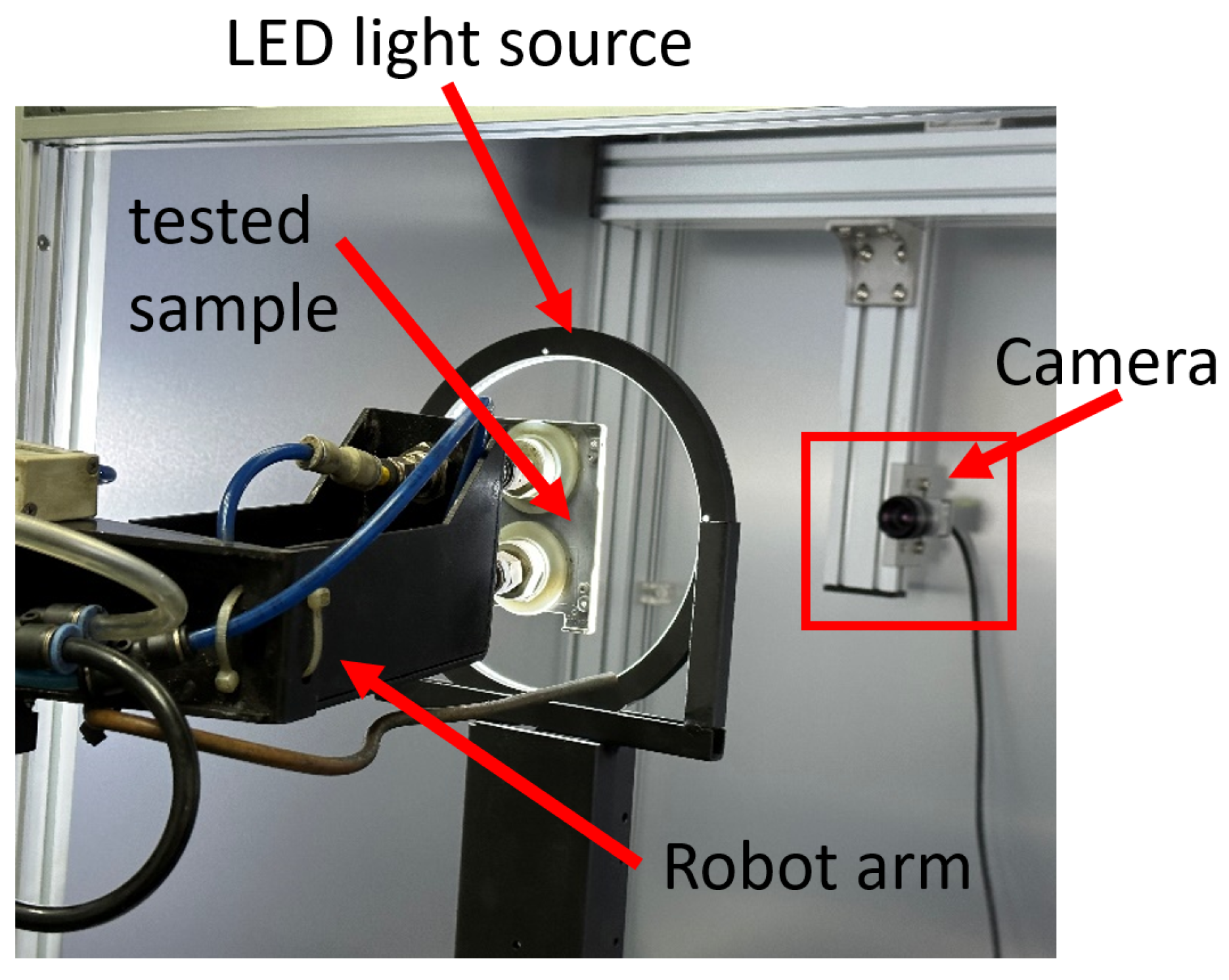
2. System Structure
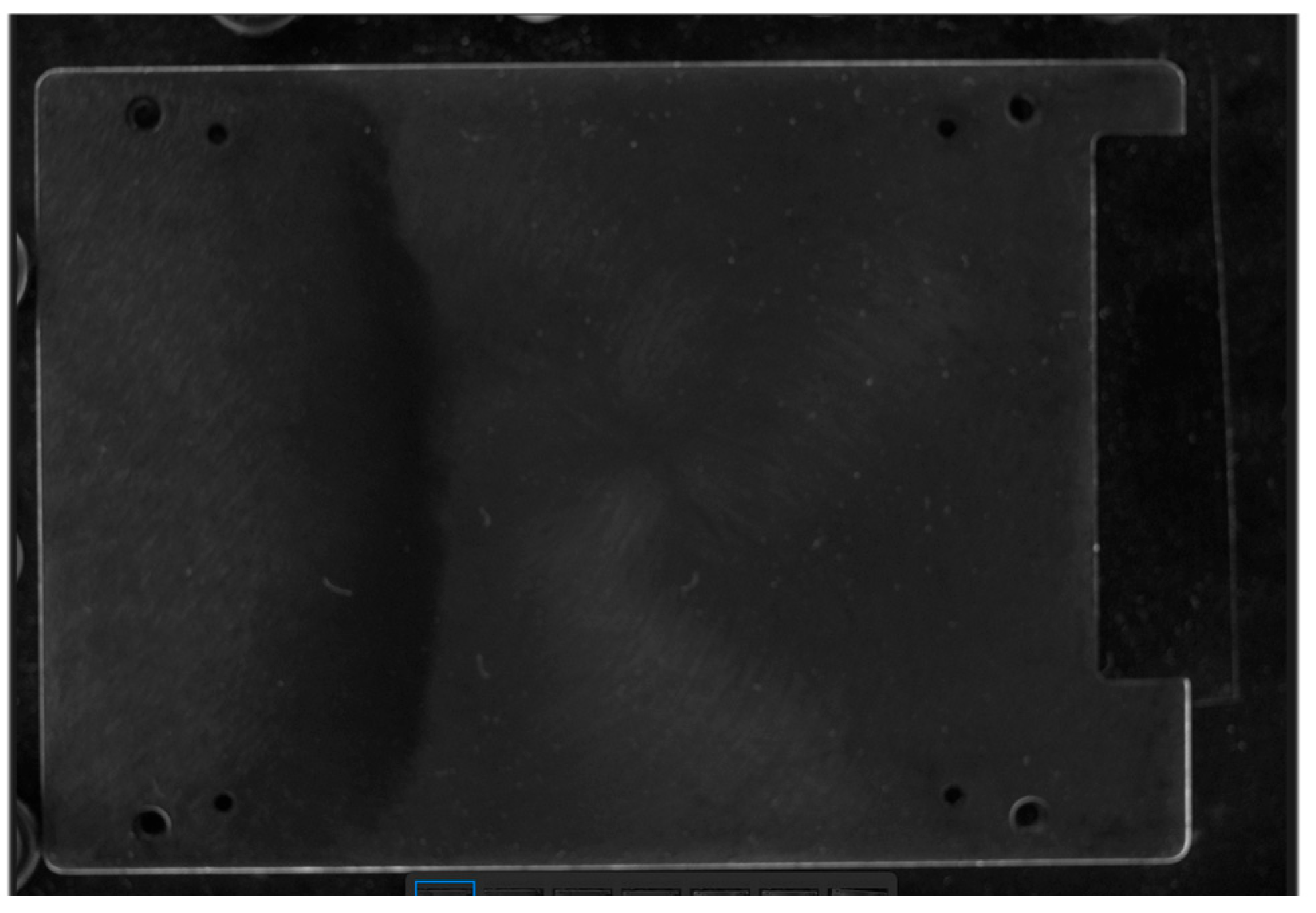
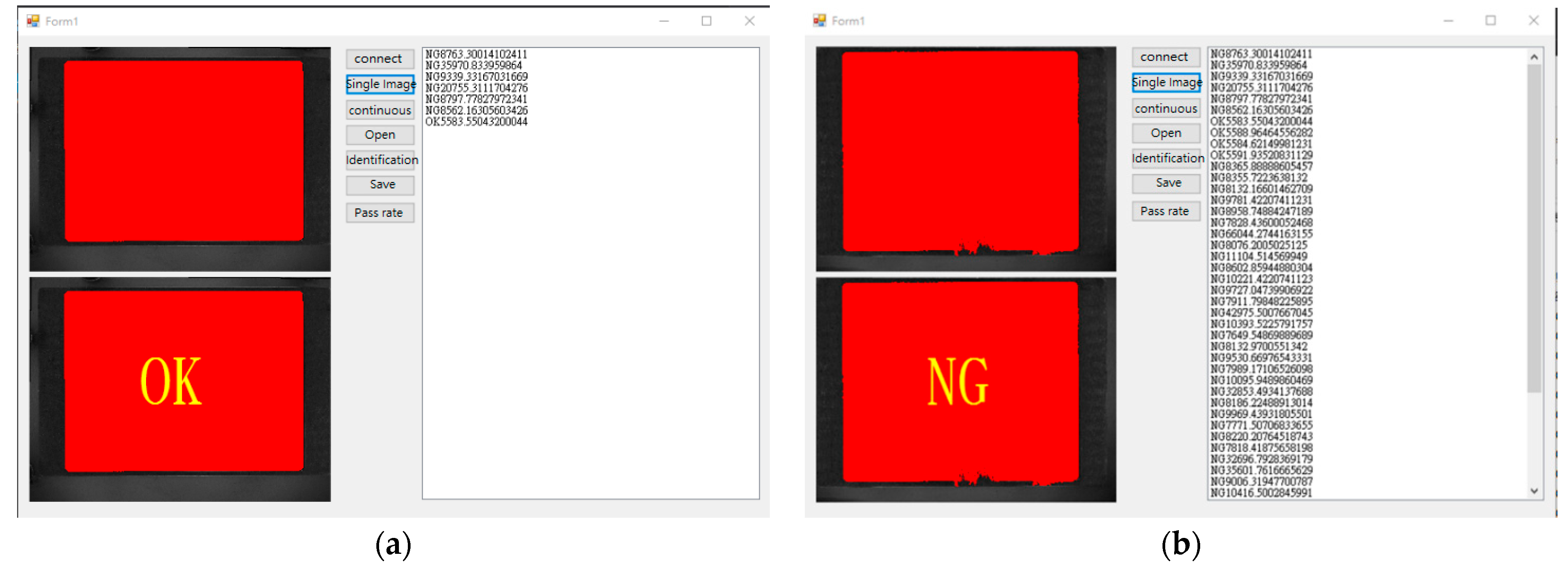
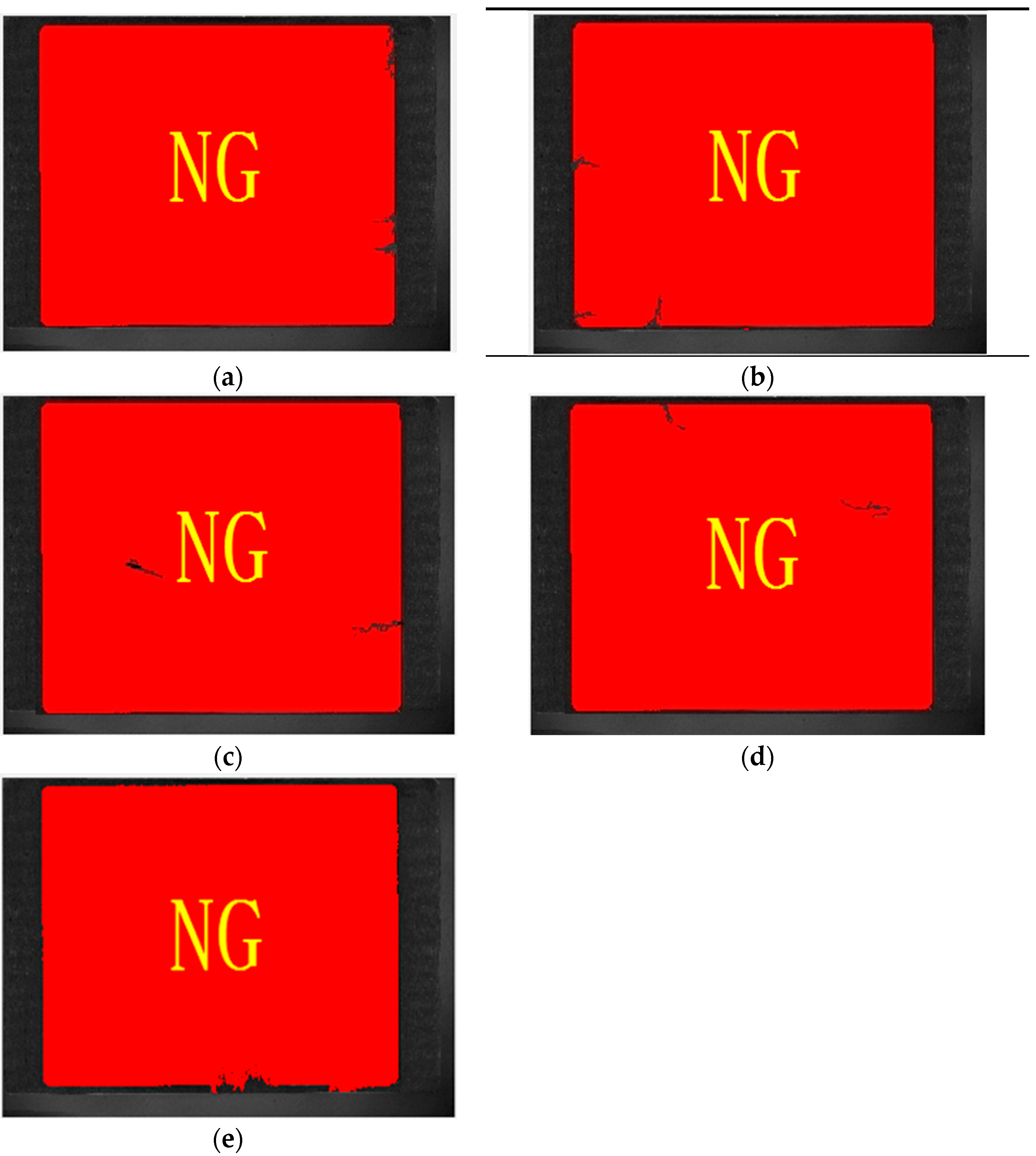
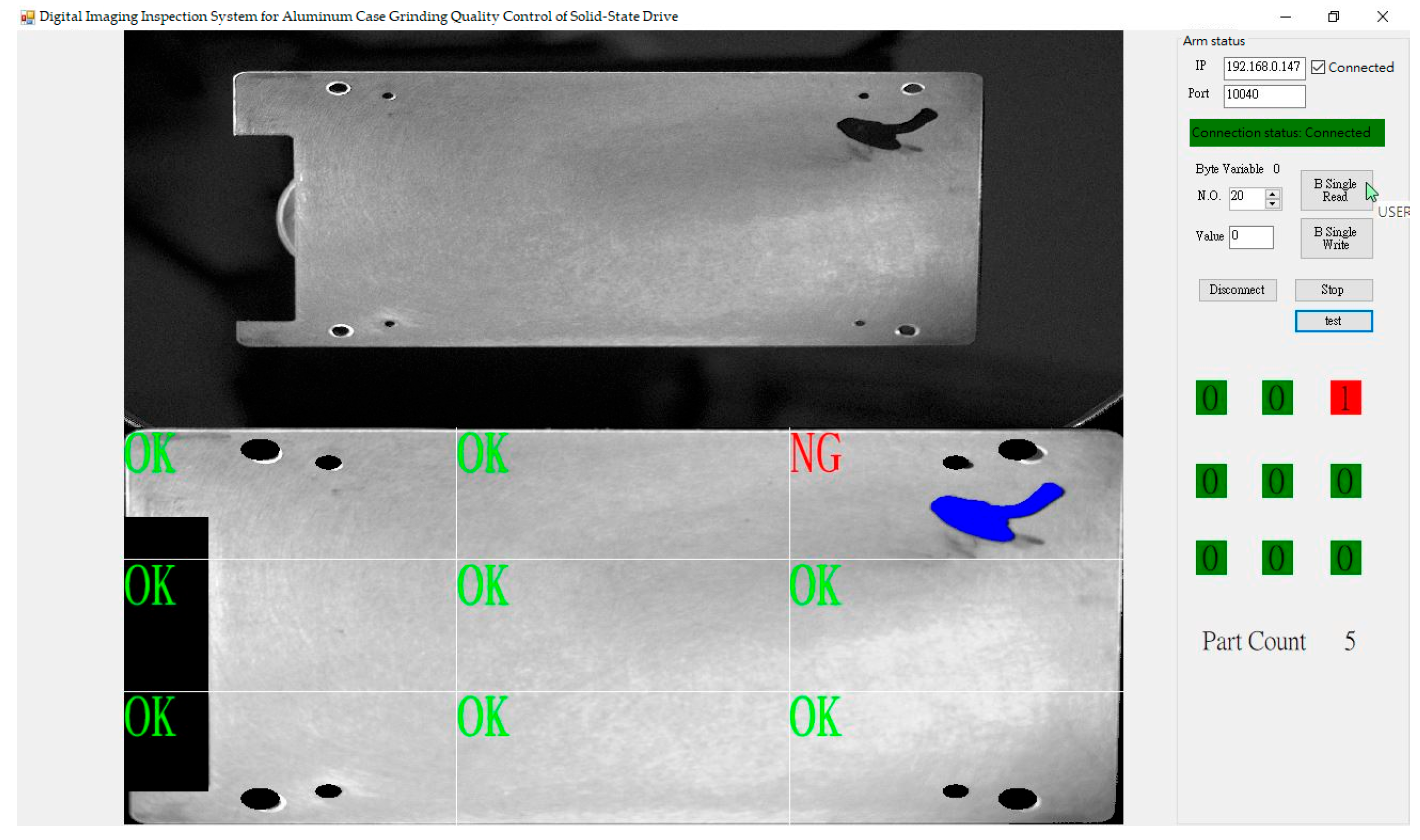
3. Experimental Results
4. Conclusions
Author Contributions
Funding
Institutional Review Board Statement
Informed Consent Statement
Data Availability Statement
Conflicts of Interest
References
- Denkena, B.; Ahlers, H.; Berg, F.; Wolf, T.; Tönshoff, H. Fast Inspection of Larger Sized Curved Surfaces by Stripe Projection. CIRP Ann. 2002, 51, 499–502. [Google Scholar] [CrossRef]
- Liao, C.-W.; Yu, J.-H.; Tarng, Y.-S. On-line full scan inspection of particle size and shape using digital image processing. Particuology 2010, 8, 286–292. [Google Scholar] [CrossRef]
- Lin, C.-S.; Huang, J.T.; Wei, T.-C.; Yeh, M.-S.; Chen, D.-C. High speed and high accuracy inspection of in-tray laser IC marking using line scan CCD with a new calibration model. Opt. Laser Technol. 2011, 43, 218–225. [Google Scholar] [CrossRef]
- Moginati, M.; Ercal, F.; Dagil, C.H.; Tsunekawa, S. Automatic PCB Inspection Algorithms: A Survey. Comput. Vis. Image Underst. 1996, 63, 287–313. [Google Scholar] [CrossRef]
- Ngan, H.Y.T.; Pang, G.K.H.; Yung, N.H.C. Automated fabric defect detection—A review. Image Vis. Comput. 2011, 29, 442–458. [Google Scholar] [CrossRef]
- Dutta, S.; Pal, S.; Mukhopadhyay, S.; Sen, R. Application of digital image processing in tool condition monitoring: A review. CIRP J. Manuf. Sci. Technol. 2013, 6, 212–232. [Google Scholar] [CrossRef]
- Lim, D.-U.; Kim, Y.-G.; Park, T.-H. SMD Classification for Automated Optical Inspection Machine Using Convolution Neural Network. In Proceedings of the 2019 Third IEEE International Conference on Robotic Computing (IRC), Naples, Italy, 28 March 2019; pp. 395–398. [Google Scholar]
- Yang, F.-S.; Ho, C.-C. Automated Optical Inspection System for O-ring based on Photometric Stereo and Machine Vision. In Proceedings of the 2020 International Symposium on Computer, Consumer and Control (IS3C), Taichung City, Taiwan, 8 April 2021; pp. 296–299. [Google Scholar]
- Zhang, M.; Sun, W.; Wang, J. Steel Surface Defect Detection Based on Adaptive Threshold Gray Transformation. In Proceedings of the 2021 IEEE International Conference on Power, Intelligent Computing and Systems (ICPIC), Shenyang, China, 29–31 July 2021; pp. 280–283. [Google Scholar]
- Li, K.S.-M.; Liao, P.Y.-Y.P.; Cheng, K.C.-C.; Chen, L.L.-Y.; Wang, S.-J.; Huang, A.Y.-A. Hidden Wafer Scratch Defects Projection for Diagnosis and Quality Enhancement. IEEE Trans. Semicond. Manuf. 2020, 34, 9–16. [Google Scholar] [CrossRef]
- Sipos, E.; Ones, A.; Ivanciu, L.-N. PCB Quality Check: Optical Inspection Using Color Mask and Thresholding. In Proceedings of the 2022 IEEE International Conference on Automation, Quality and Testing, Robotics (AQTR), Cluj-Napoca, Romania, 19–21 May 2022; pp. 1–5. [Google Scholar]
- Tahir, M.N.; Khalid, Z.; Aslam, A. Online, Real-time and Robust Detection and Localization of Foreign Objects on Paper Surface using Machine Vision and Clustering. In Proceedings of the 2022 28th International Conference on Mechatronics and Machine Vision in Practice (M2VIP), Nanjing, China, 16–18 November 2022; pp. 1–6. [Google Scholar]
- Sirvent, J.L.G.; Rosa, F.L.D.L.; Sanchez-Reolid, R.; Fernandez-Caballero, A.; Morales, R. Optimal Feature Selection for Defect Classification in Semiconductor Wafers. IEEE Trans. Semicond. Manuf. 2022, 35, 324–331. [Google Scholar] [CrossRef]
- Li, K.S.-M.; Chen, L.L.-Y.; Cheng, K.C.-C.; Liao, P.Y.-Y.; Wang, S.-J.; Huang, A.Y.-A.; Chou, L.; Tsai, N.C.-Y.; Lee, C.-S. TestDNA-E: Wafer Defect Signature for Pattern Recognition by Ensemble Learning. IEEE Trans. Semicond. Manuf. 2022, 35, 372–374. [Google Scholar] [CrossRef]
Disclaimer/Publisher’s Note: The statements, opinions and data contained in all publications are solely those of the individual author(s) and contributor(s) and not of MDPI and/or the editor(s). MDPI and/or the editor(s) disclaim responsibility for any injury to people or property resulting from any ideas, methods, instructions or products referred to in the content. |
© 2025 by the authors. Licensee MDPI, Basel, Switzerland. This article is an open access article distributed under the terms and conditions of the Creative Commons Attribution (CC BY) license (https://creativecommons.org/licenses/by/4.0/).
Share and Cite
Chen, C.-J.; Tsai, C.-F. Digital Imaging Inspection System for Aluminum Case Grinding Quality Control of Solid-State Drive. Eng. Proc. 2025, 92, 96. https://doi.org/10.3390/engproc2025092096
Chen C-J, Tsai C-F. Digital Imaging Inspection System for Aluminum Case Grinding Quality Control of Solid-State Drive. Engineering Proceedings. 2025; 92(1):96. https://doi.org/10.3390/engproc2025092096
Chicago/Turabian StyleChen, Chun-Jen, and Cheng-Feng Tsai. 2025. "Digital Imaging Inspection System for Aluminum Case Grinding Quality Control of Solid-State Drive" Engineering Proceedings 92, no. 1: 96. https://doi.org/10.3390/engproc2025092096
APA StyleChen, C.-J., & Tsai, C.-F. (2025). Digital Imaging Inspection System for Aluminum Case Grinding Quality Control of Solid-State Drive. Engineering Proceedings, 92(1), 96. https://doi.org/10.3390/engproc2025092096