Proceeding Paper

A Low-Power, Fast Transient Response Low-Dropout Regulator Featuring Bi-Directional Level Shifting for Sensor Applications †

School of Electronic and Optical Engineering, Nanjing University of Science and Technology, Nanjing 210094, China
*
Author to whom correspondence should be addressed.
Presented at the 11th International Electronic Conference on Sensors and Applications (ECSA-11), 26–28 November 2024; Available online: https://sciforum.net/event/ecsa-11.
Eng. Proc. 2024, 82(1), 53; https://doi.org/10.3390/ecsa-11-20349
Published: 25 November 2024

Abstract

:
Wireless sensor network (WSN) is an important component of healthcare. The design of the power management unit for WSN poses significant challenges, as it not only needs to achieve good current efficiency but also requires high power supply rejection (PSR) and good load transient performance. This paper presents a low-dropout regulator (LDO) with a low quiescent current and fast transient response to adequately meet the power supply requirements of WSN systems. To ensure system stability and reduce voltage spikes during load transients, an adaptive frequency compensation network is integrated into the circuit. Additionally, the LDO incorporates a level shifter that facilitates the bi-directional transmission of voltage signals across different power systems. The proposed LDO is designed and simulated in a 180 nm BCD process. It operates under a wide input voltage range from 0.8 V to 5.5 V, supports maximum load currents of up to 500 mA, and allows output voltages to vary from 0.8 V to 3.6 V by adjusting the feedback resistance. As a result of implementing the adaptive frequency compensation circuit, the overshoot and undershoot voltages at an output voltage of 1 V are measured to be only 23 mV and 5 mV, respectively. Moreover, the LDO achieves a PSR of −83 dB for bias voltage and −91 dB for input voltage at 1 kHz. The level shifter’s highest working frequency can reach 20 MHz under supply voltages (Vin = 1.65 V to 5.5 V; Vout = 3.6 V), thereby enabling high-speed data transmission. Finally, the LDO consumes a quiescent current of 42 μA while incorporating a bandgap reference circuit and other auxiliary circuits.

1. Introduction

Wireless sensor nodes have been widely adopted in various fields, including smart homes, military communications, and medical care, due to their advantages of compact size, low power consumption, high cost-effectiveness, and ease of installation [1,2]. Figure 1 illustrates a wireless sensor network system used for physiological monitoring, where each user wears multiple wireless sensor nodes for physiological signal acquisition. Due to the limited area (≈50 mm × 30 mm) of each node, there are stringent requirements regarding size and power consumption.
The operation of wireless sensor network (WSN) nodes involves two distinctly different load conditions: light-load operation for sensors and heavy-load operation for transceivers [3]. This requires the power management unit to exhibit good transient performance while also meeting low power consumption and high-power supply rejection ratio (PSR) requirements. A low dropout regulator (LDO) can generate a clean, high-precision voltage that is independent of the input voltage. Additionally, they occupy less space compared to switching regulators, as they require fewer external components. All these advantages make LDO the ideal choice for power supply in WSN systems.
In the past, several standard approaches have been adopted to either reduce quiescent current or enhance transient response; however, they could not satisfy all requirements simultaneously. For instance, reference [4] proposed a load transient-enhanced circuit based on an FVF circuit configuration for an LDO that features a quiescent current of only 204 nA. However, being limited to a maximum load current of only 10 mA does not meet the load requirements of WSN nodes. In reference [5], the author proposed a capacitorless LDO that significantly enhances PSR through an adaptive supply ripple cancellation (ASRC) technique. Measurement results indicated that the proposed LDO achieves a PSR of less than −36 dB across all frequencies from 10 kHz to 1 GHz, demonstrating its superior performance and robustness. However, it consumes over 200 µA of quiescent current, resulting in very low current efficiency.
In the wireless sensor node illustrated in Figure 1, a system-on-chip (SoC) wireless control module is configured to connect with the parameter collection module via the inter-integrated circuit (I2C) interface, facilitating seamless parameter collection and transmission. However, different systems often operate at varying supply voltages, which complicates data transfer between them. This situation necessitates the use of level shifters to resolve the issue. Currently, most commercially available level shifters are standalone chips that require careful circuit planning during system design, thereby increasing both design costs and complexity.
To address the issues mentioned earlier, we propose a low dropout linear regulator chip that features level-shifting capabilities. This chip not only meets the power supply requirements of wireless sensor networks but also serves as a bridge for signal transmission between systems operating at different voltage levels.

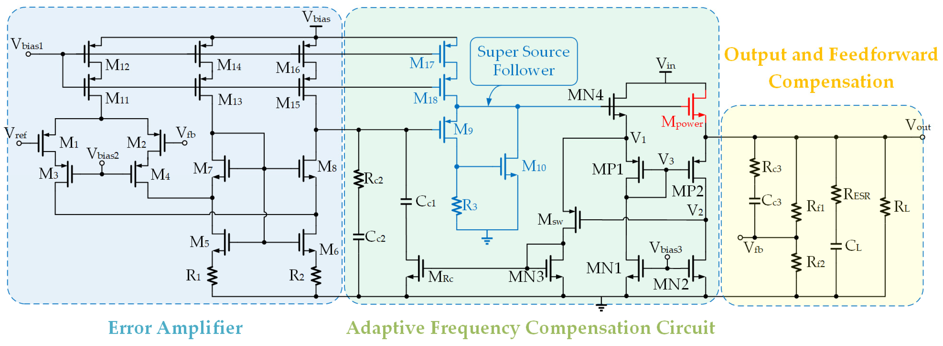
2. Design of the Proposed Low-Dropout Regulator

Figure 2 illustrates the block diagram of the proposed LDO, which primarily consists of an error amplifier (EA), a buffer, a power MOSFET, an adaptive frequency compensation, and a level shifter. The error amplifier ensures the accuracy and stability of the output voltage. The super source follower (SSF) buffer, along with the adaptive frequency compensation module, contributes to the overall stability of the system. This enhancement guarantees that the output voltage remains stable during transient changes in load current while significantly reducing fluctuations caused by load variations. We utilize NMOS as the power transistor to enhance transient response while minimizing the layout area. Furthermore, to achieve a single-chip power supply and level shifting, a level-shifting module is integrated into the LDO, facilitating signal transmission between the input voltage (Vin) and output voltage (Vout) domains.

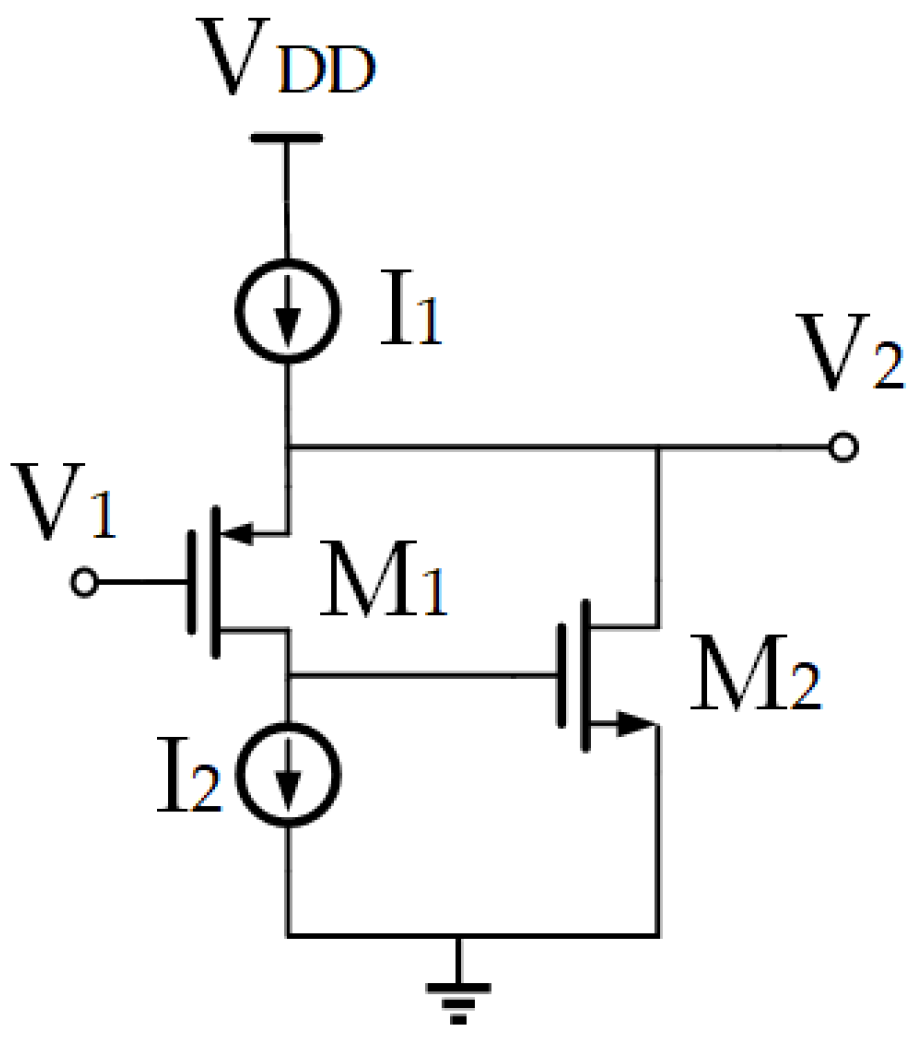
2.1. Super Source Follower

The SSF is designed as a buffer, drawing inspiration from the traditional source follower configuration. To accommodate an output load current of 500 mA, the required power transistor must be sufficiently large, which leads to increased parasitic capacitance at the gate of the power transistor. Additionally, to meet the output linearity requirements, the error amplifier must possess a sufficiently high gain, resulting in a significant increase in its output impedance. If the output of the error amplifier is directly connected to the gate of the power transistor, it would introduce a low-frequency pole that could compromise the system’s stability. Therefore, it is essential to place a buffer between the error amplifier and the gate of the power transistor to achieve pole separation and enhance the system’s slew rate. This paper utilizes the SSF illustrated in Figure 3, with its output impedance represented by Equation (1).
Rout = 1 ( g m 1 + g m b 1 ) g m 2 ( r o 1 / / r o I 1 )
where gm1 and gm2 represent the transconductance of transistors M1 and M2, respectively. gmb1 denotes the bulk transconductance of M1, while ro1 and roI1 refer to the output resistances of M1 and the current source I1, respectively.

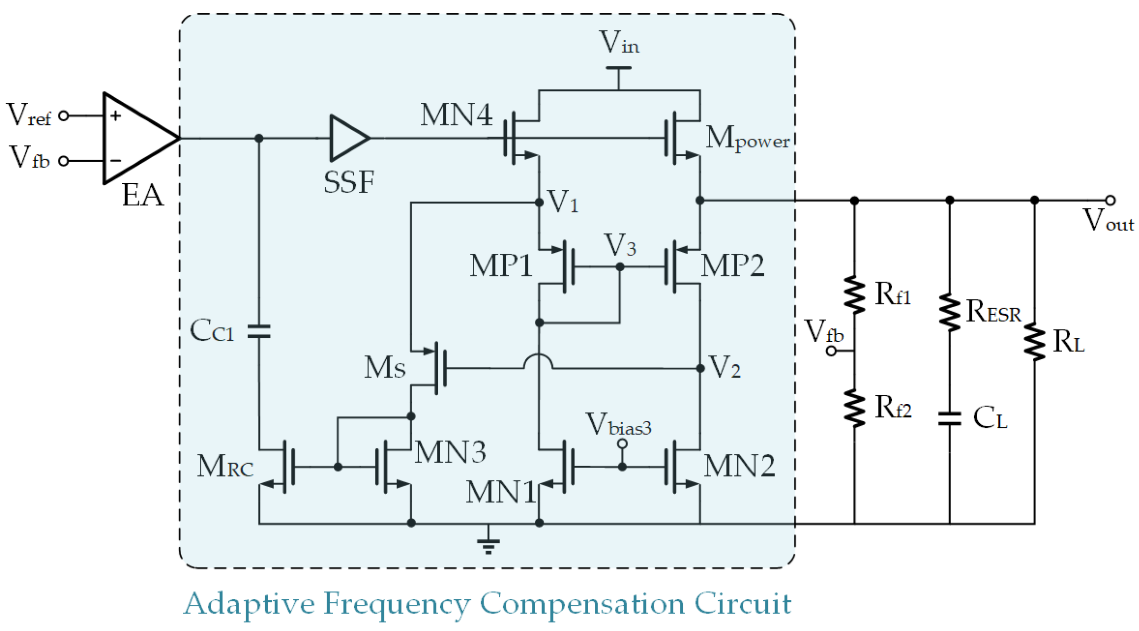
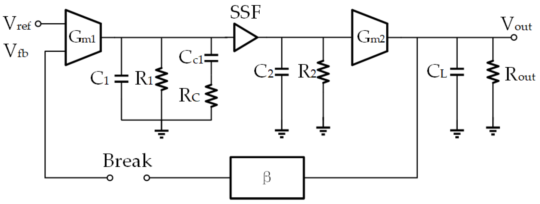
2.2. Adaptive Frequency Compensation

Relying solely on the SSF is insufficient to ensure that the LDO maintains stability under various load conditions. As load current changes, the output impedance at the output terminal will also vary. With the output capacitance remaining constant, an increase in load impedance will cause the output pole to move toward lower frequencies, thereby reducing the phase margin. To ensure the LDO remains stable during fluctuations in load current, this paper introduces an adaptive frequency compensation circuit built upon the SSF design. The specific design of this frequency compensation circuit is illustrated in Figure 4.
In this circuit, Mpower acts as the power transistor, while MN4 proportionally replicates the current from the Mpower. The equivalent resistance of MRC, in conjunction with capacitor Cc1, is used for zero frequency compensation within the circuit. Due to the characteristics of the current mirror, when the load current is low, the source voltages of Mpower and MN4 are equal. However, as the load current increases, the gate voltage of the power transistor and the source voltage of MN4 also rise. To maintain the current through MP1, voltage V3 will increase, causing MP2 to enter cutoff mode. At this point, the voltage at V2 decreases, resulting in the conduction of Msw, allowing the current from MN4 to flow through Msw. Consequently, the operating state of the MRC transistor transitions from cutoff to the linear region, reducing its equivalent impedance and producing a zero within the unity gain bandwidth together with Cc1.
Figure 5 illustrates the small-signal model of the LDO after frequency compensation, where the output impedance of the error amplifier is represented as R1, and the output capacitance is equivalent to C1. Under the influence of the SSF, the equivalent impedance at the gate of the power transistor is significantly reduced. C2 represents the equivalent capacitance at the output of the SSF, primarily arising from the parasitic capacitance of the power transistor. To ensure the transient performance of the LDO, a relatively large capacitor CL (typically on the order of microfarads) is usually added at the output. Additionally, the output impedance Rout varies with changes in load current, thereby affecting the system’s stability. Gm1 and Gm2 represent the transconductances of the EA and the Mpower, respectively. In the adaptive compensation circuit, the compensation capacitor is denoted as Cc1, while Rc is the equivalent resistance of the MRC, which changes with variations in load. Finally, β represents the feedback factor.
Based on the description above and the small signal model, we can derive the open-loop transfer function of the system as follows:
T ( s ) = β G m 1 G m 2 R 1 R out ( 1 + R c C c 1 S ) ( 1 + R out C LS ) ( 1 + R 2 C 2 S ) [ R 1 R c C c 1 C 1 S 2 + ( R 1 C 1 + R c C c 1 + R 1 C c 1 ) S + 1 ]
When the transistor MRC operates in the linear region, the resistance R1 is much greater than Rc, and the capacitance Cc1 is significantly larger than C1, then the transfer function can be simplified as follows:
T ( s ) = β G m 1 G m 2 R 1 R out ( 1 + R c C c 1 S ) ( 1 + R out C LS ) ( 1 + R 2 C 2 S ) ( 1 + R 1 C c 1 S ) ( 1 + R c C c 1 S )
This allows us to obtain the zero and poles of the system, as shown in Table 1:
The open-loop gain is shown in Figure 6. As the load current decreases, the output impedance Rout and the equivalent resistance Rc of the MOSFET MRC gradually increase, which primarily affects the positions of ωp2, ωp3, and ωz1 in the frequency response. However, when the load current is very low, Msw turns off, causing MRC to enter the cutoff region. Additionally, when there are significant variations in the load, MRC struggles to remain in the linear operating region and is prone to entering saturation [6]. The combined effects of these factors lead to a substantial increase in the equivalent resistance of MRC, resulting in an unstable state for the system.
Therefore, modifications were made to the circuit in Figure 4 by adding an additional zero compensation at the output of the error amplifier and simultaneously introducing an output feedforward capacitor. Figure 7 shows the complete LDO schematic with the adaptive frequency compensation circuit. The error amplifier is designed as a folded cascode amplifier, and the current mirror PMOS transistors operate in the sub-threshold region to reduce static power consumption and improve DC gain. To minimize layout area and enhance load transient response, NMOS transistors are used as power devices in the circuit. Additionally, the circuit employs a dual power supply to reduce the dropout voltage.
In conditions of low load current, ωz1 and ωp3 approximately cancel each other out. At this point, the compensation resistor Rc2 and compensation capacitor Cc2 create a zero within the unity gain bandwidth, effectively replacing the positions of Cc1 and Rc, thereby maintaining the stability of the system. Additionally, the feedforward compensation capacitor Cc3 and compensation resistor Rc3 introduce another zero. By adjusting the values of these resistors and capacitors, the zeros can be positioned within the unity gain bandwidth, effectively enhancing both gain and phase, thus improving the overall phase margin of the loop.

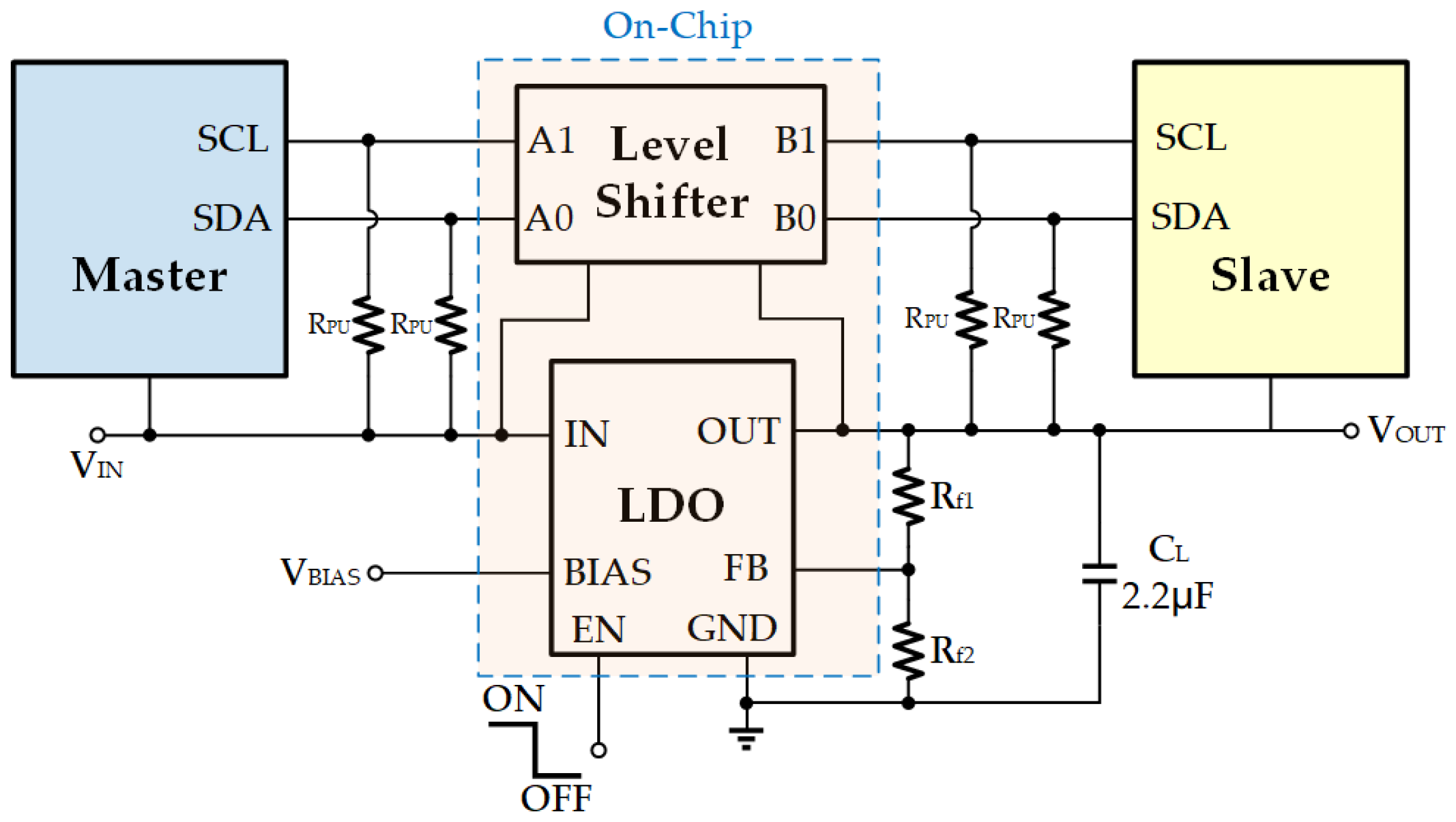
2.3. Integrated LDO and Level Shifter

In a multi-voltage system, such as a WSN node or an Internet of Things (IoT) device, when a lower voltage-powered module directly drives a higher voltage-powered module, the significant voltage difference may prevent the PMOS transistor in the load unit from turning off completely. This can lead to substantial leakage current and noticeable leakage power consumption. In severe cases, it could even result in the malfunctioning of the chip. Therefore, a level shifter must be inserted between different voltage domains. Thanks to our proposed LDO, which features a wide input voltage range and adjustable output voltage, we have integrated a level shifter suitable for open-drain outputs that support bidirectional transmission into this LDO, as illustrated in Figure 8. In this block diagram, we connect the input voltage Vin to the power supply of side A of the level shifter and the output voltage Vout to the power supply of side B. This allows us to achieve both power supply for the master-slave devices and data transfer between them using a single chip, thereby simplifying circuit system design and reducing costs.

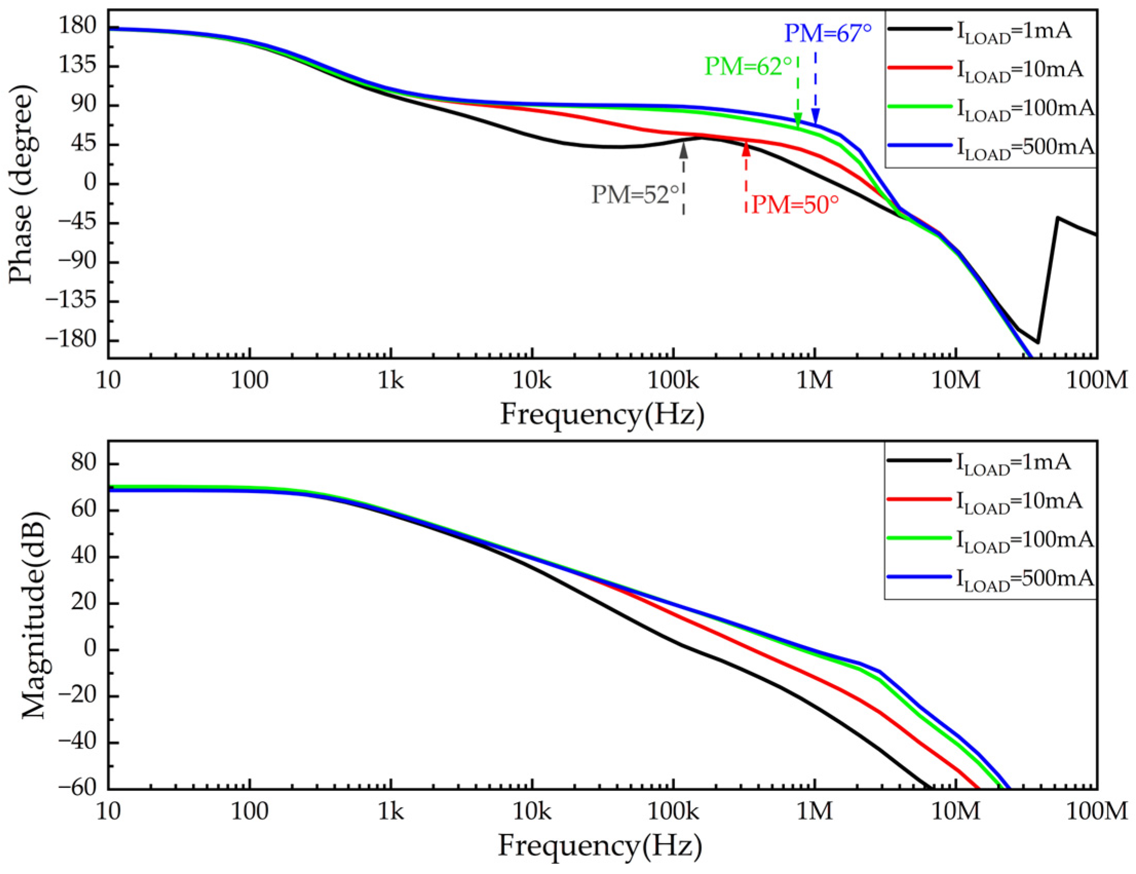
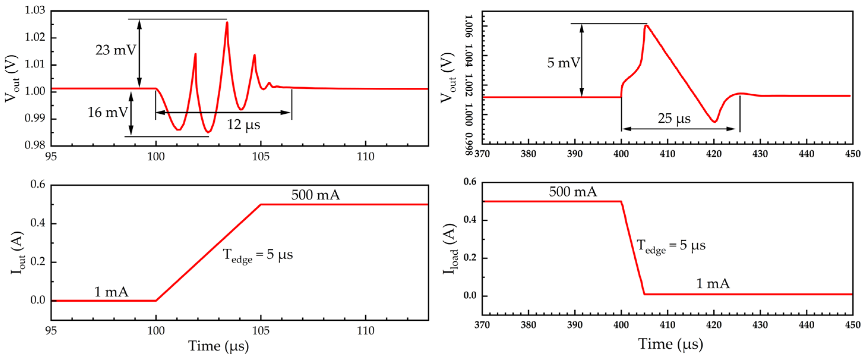
3. Simulation Results and Discussion

The proposed LDO is designed using a 180 nm BCD process. Figure 9 shows the layout of this design, with an overall area of 1108 µm × 686 µm. This design includes a bandgap reference, an error amplifier, an adaptive frequency compensation circuit with a super source follower, the power transistor, and the level shifter.
We set the input voltage range from 1.3 V to 5.5 V, the output voltage at 1 V, and the load capacitance at 2.2 µF for the simulation. Figure 10 illustrates the open-loop frequency response of the LDO under various load conditions. It is evident that changes in load significantly affect stability. Thanks to the adaptive frequency compensation circuit, the phase margin varies between 50° and 67°, indicating that the system can maintain stability. However, this comes at the cost of reduced bandwidth, demonstrating the trade-off between stability and speed.
The proposed LDO uses an NMOS transistor as the power device and employs a dual power supply to reduce dropout voltage, necessitating consideration of the PSR of both Vbias and Vin. Figure 11 illustrates the simulated PSR performance of the proposed LDO under a load current of 150 mA. Thanks to the design of the common-source and cascode amplifiers along with the feedforward circuit, the PSR of Vbias reaches −83 dB at 1 kHz. Additionally, with the effect of the NMOS power transistor, the PSR of Vin also attains −91 dB at 1 kHz.
The WSN node experiences variations between heavy and light loads during operation, which places high demands on the transient performance of the LDO. Figure 12 presents the transient simulation results when the load changes from 1 mA to 500 mA, with both the rise and fall times set at 5 µs and an output voltage of 1 V. During the load current increase, the maximum voltage swing is 23 mV; conversely, during the load current decrease, the overshoot of output voltage is 5 mV, with recovery times of 12 µs and 25 µs, respectively.
We have functionally integrated a level shifter into the LDO. Figure 13 illustrates the output simulation results of this level shifting module, where the input voltage Vin is set at 5 V, with output voltages Vout of 3.6 V and 1.8 V. The results indicate that the maximum data rate can reach 20 MHz when voltage translating from 5 V to 3.6 V and up to 10 MHz when voltage translating from 5 V to 1.8 V.
The figure of merit (FOM) in [7] is adopted to evaluate the transient response of an LDO with respect to the change in the load current. The performance comparison with previously reported LDOs is summarized in Table 2.
Table 2. Performance summary and comparison with different LDOs.
Parameter[8][9][10][11]This Work
Published date (year)20202020202420242024
Technology (nm)180 180600110180
Vin (V)1.4–1.85.52.2–5.54–4.50.8–5.5
Vout (V)1.21.5–5.251.8–3.31.850.8–3.6
ΔVout (mV)203638.627123
Cout (μF)4.72.2112.2
Iq (μA)13.55.6–35.69.65742
Iload, max (mA)150250150300500
Iload, min (mA)0.1NANANA1
Line reg (mV/V)7.78510.20110.62
Load reg (mV/mA)0.07500.11200.060.002670.0018
Vin PSR @ freq(dB)−30 dB
@100 Hz
−70 dB
@1 MHz
−71 dB
@1 KHz
−22 dB
@1 MHz
−91 dB
@1 KHz
Vbias PSR @ freq(dB)NANANANA−83@1 KHz
FOM 1 (ps)1047.1016.471718.5
1 FOM = CoutΔVoutIq/Iload, max2.

4. Conclusions

This paper proposes a low-power LDO circuit with fast transient response and high PSR specifically designed for wireless sensor network nodes. The proposed LDO utilizes an adaptive frequency compensation circuit along with additional zero and feedforward compensation to address the design challenges of stability and load transient response. During the transient change of load current from 1 mA to 500 mA within 5 µs, the maximum swing of the output voltage is only 23 mV (with an output voltage of 1 V), and it can recover stability within 25 µs. Thanks to the use of a folded cascode error amplifier and NMOS transistor as a power device, the circuit achieves sufficient loop gain while maintaining good power supply rejection performance. Functionally integrating a level-shifting module into the LDO expands its application range, simplifies external design, and meets the demands for system integration and miniaturization, showing better prospects in applications such as sensors and IoT devices.

Author Contributions

Conceptualization, H.H. and J.C.; methodology, H.H. and J.C.; software, H.H.; validation, H.H. and J.C.; formal analysis, H.H.; investigation, H.H. and J.C.; resources, J.C.; data curation, H.H.; writing—original draft preparation, H.H.; writing—review and editing, J.C.; supervision, J.C.; project administration, J.C.; funding acquisition, J.C. All authors have read and agreed to the published version of the manuscript.

Funding

This research received no external funding.

Institutional Review Board Statement

Not applicable.

Data Availability Statement

The original contributions presented in the study are included in the paper, further inquiries can be directed to the corresponding author.

Conflicts of Interest

The authors declare no conflicts of interest.

References

  1. Chen, S.-L.; Lee, H.-Y.; Chen, C.-A.; Huang, H.-Y.; Luo, C.-H. Wireless Body Sensor Network With Adaptive Low-Power Design for Biometrics and Healthcare Applications. IEEE Systems Journal 2009, 3, 398–409. [Google Scholar] [CrossRef]
  2. Hao, Y.; Foster, R. Wireless Body Sensor Networks for Health-Monitoring Applications. Physiol. Meas. 2008, 29, R27–R56. [Google Scholar] [CrossRef]
  3. Gweon, S.; Lee, J.; Kim, K.; Yoo, H.-J. 93.8% Current Efficiency and 0.672 Ns Transient Response Reconfigurable LDO for Wireless Sensor Network Systems. In Proceedings of the 2019 IEEE International Symposium on Circuits and Systems (ISCAS), Sapporo, Japan, 26–29 May 2019; pp. 1–5. [Google Scholar]
  4. Mii, K.; Nagahama, A.; Watanabe, H. Ultra-Low Quiescent Current LDO with FVF-Based Load Transient Enhanced Circuit. IEICE Trans. Electron. 2020, E103.C, 466–471. [Google Scholar] [CrossRef]
  5. Lim, Y.; Lee, J.; Park, S.; Jo, Y.; Choi, J. An External Capacitorless Low-Dropout Regulator With High PSR at All Frequencies From 10 kHz to 1 GHz Using an Adaptive Supply-Ripple Cancellation Technique. IEEE J. Solid-State Circuits 2018, 53, 2675–2685. [Google Scholar] [CrossRef]
  6. Gao, J.; Wang, X.; Chen, B.; Liu, H.; Li, X.; Guo, P. A High-Input-Voltage Wide-Load LDO with Improved Load-Dependent Zero Mobile Compensation. In Proceedings of the 2022 IEEE 65th International Midwest Symposium on Circuits and Systems (MWSCAS), Fukuoka, Japan, 7–10 August 2022; pp. 1–5. [Google Scholar]
  7. Hazucha, P.; Karnik, T.; Bloechel, B.A.; Parsons, C.; Finan, D.; Borkar, S. Area-Efficient Linear Regulator with Ultra-Fast Load Regulation. IEEE J. Solid-State Circuit 2005, 40, 933–940. [Google Scholar] [CrossRef]
  8. Ming, X.; Liang, H.; Zhang, Z.-W.; Xin, Y.-L.; Qin, Y.; Wang, Z. A High-Efficiency and Fast-Transient Low-Dropout Regulator With Adaptive Pole Tracking Frequency Compensation Technique. IEEE Trans. Power Electron. 2020, 35, 12401–12415. [Google Scholar] [CrossRef]
  9. Joshi, K.; Manandhar, S.; Bakkaloglu, B. A 5.6 μ A Wide Bandwidth, High Power Supply Rejection Linear Low-Dropout Regulator With 68 dB of PSR Up To 2 MHz. IEEE J. Solid-State Circuit 2020, 55, 2151–2160. [Google Scholar] [CrossRef]
  10. Fan, H.; Feng, L.; Diao, X.; Xie, X.; Wang, C.; Li, G.; Wei, Q.; Qiao, F.; Feng, Q.; Bonizzoni, E. A Fast Transient LDO Regulator Featuring High PSRR Over 100-kHz Frequency Range With Adaptive, Dynamic Biasing, and Current Mode Feed-Forward Amplifier. IEEE Trans. Circuits Syst. II-Express Briefs 2024, 71, 1764–1768. [Google Scholar] [CrossRef]
  11. Tang, J.; Fan, B.; Liu, H.; Li, M.; Qin, K. Multi-Zero Pole Dynamically Compensated LDO with Low Quiescent Current. AEU Int. J. Electron. Commun. 2024, 184, 155423. [Google Scholar] [CrossRef]
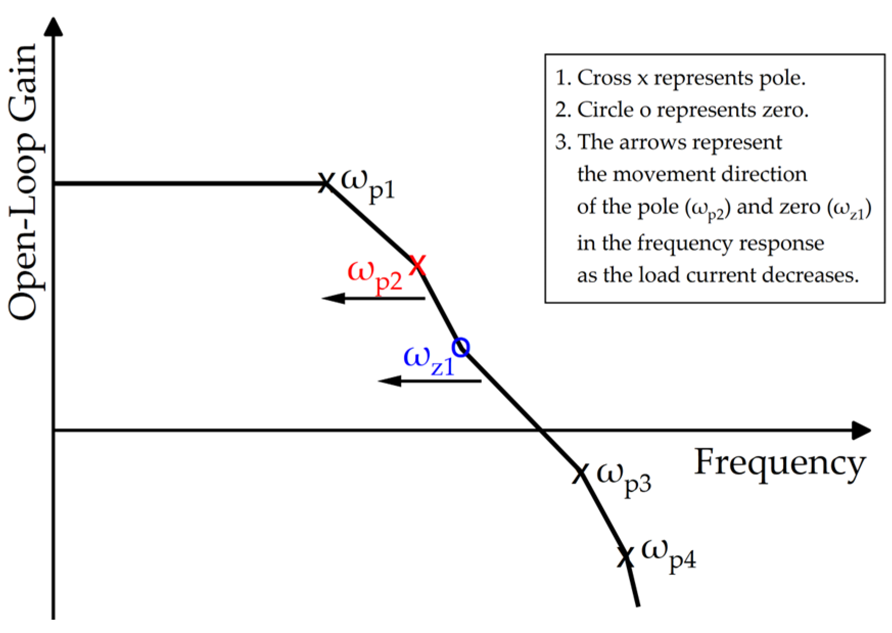
Figure 1. Overall structure of the physiological monitoring wireless sensor network.
Engproc 82 00053 g001
Figure 2. Block diagram of the proposed LDO.
Engproc 82 00053 g002
Figure 3. The schematic of the super source follower.
Engproc 82 00053 g003
Figure 4. The schematic of the adaptive frequency compensation circuit.
Engproc 82 00053 g004
Figure 5. Small signal model of the LDO with adaptive frequency compensation circuit.
Engproc 82 00053 g005
Figure 6. Loop gain of the LDO with adaptive frequency compensation circuit.
Engproc 82 00053 g006
Figure 7. The complete schematic of the proposed LDO.
Engproc 82 00053 g007
Figure 8. Block diagram of the proposed LDO with level shifter.
Engproc 82 00053 g008
Figure 9. Layout of the proposed LDO.
Engproc 82 00053 g009
Figure 10. Simulated open-loop gain and phase response at different loads.
Engproc 82 00053 g010
Figure 11. Simulated PSR of the proposed LDO.
Engproc 82 00053 g011
Figure 12. Simulated load transient response of the proposed LDO.
Engproc 82 00053 g012
Figure 13. Simulated results of the level shifter with different Vin and Vout: (a) Vin = 5 V, Vout = 3.6 V; (b) Vin = 5 V, Vout = 1.8 V.
Engproc 82 00053 g013
Table 1. Zero and poles of the compensated LDO.
ParameterEquation
ωp11/R1Cc1
ωp21/RoutCL
ωp31/RcC1
ωp41/R2C2
ωz11/RcCc1
Disclaimer/Publisher’s Note: The statements, opinions and data contained in all publications are solely those of the individual author(s) and contributor(s) and not of MDPI and/or the editor(s). MDPI and/or the editor(s) disclaim responsibility for any injury to people or property resulting from any ideas, methods, instructions or products referred to in the content.

