1. Introduction
In the present application, a two-quadrant DC–DC converter is also described as a DC chopper. It is a well-known fundamental switching circuit stage, and it is widely used in areas where bidirectional energy transfer is required—motor control with regenerative braking, battery charging in renewable energy systems, microgrid power distribution, and more [
1,
2]. With the application of various control methods, it is possible to obtain the energy transfer to the load and vice versa [
3]. In practical implementations, there are two main circuit topologies: step-down and step-up DC–DC converters. The average quantities are adjusted when the switching state is controlled.
Different mathematical methods are used to calculate the main values of the ripple bias and voltage drop at the converter stage components [
4,
5]. A simple circuit topology with advanced control can obtain better results with a proper output filter setup. Nowadays, robust algorithms are used to increase the overall circuit efficiency [
6,
7]. Furthermore, in practice, there are some implementations where the control frequency is also variable [
8]. This again requires an advanced approach in the circuit design in order to obtain proper electromagnetic field (EMF) and efficiency characteristics [
9]. Adjustment of the output LC filter configuration and values could increase the overall circuit effectiveness [
10].
Most of the above-quoted applications demand advanced circuit designs and complex control in order to obtain the required output parameters for each case. The presented study is focused on proper filter estimation. In many cases, the overall device characteristics are affected by the filter parameters. Considering this fact is crucial for applications with wide dynamic ranges and variable loads. More of these conditions are presented in practical implementations as battery charging, where the state of the charge and therefore its characteristics change in several instances. The authors examine the circuit output behavior (the gain at the rated frequency) due to the load factor variation and extract the data for the converter steady state of the operation.
2. Circuit Topology and Calculation Methods
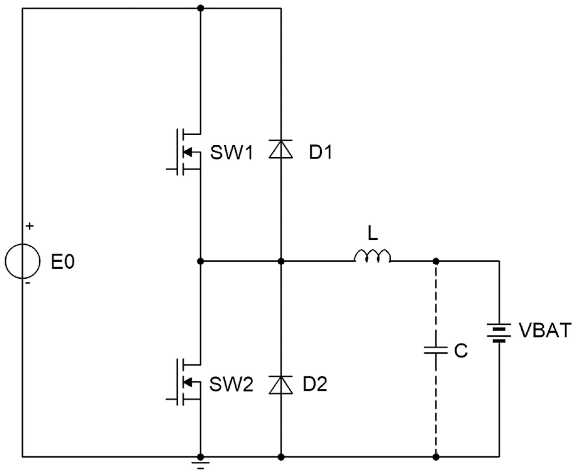
A DC–DC converter in which the power can flow from the source to the load and vice versa while the load voltage maintains the same polarity is referred to as a two-quadrant converter (
Figure 1). In other words, the two-quadrant converter operates in the 1st and the 4th quadrants. Consider that the power can only flow from the load toward the source when the load has an active component such as a battery (battery charger system) or the back EMF of a DC electric drive.
Output voltage of the converter is normally regulated by two different methods, widespread in practice: pulse width modulation control (PWM) at constant frequency operation or variable frequency control (VF)
. For PWM control,
is changed while keeping operating frequency
f and period
T constant. Output voltage is varied by adjusting the ON time
. Pulse sequence for this method is shown in
Figure 2a. For VF control, operating frequency
f’ is changed, keeping either
or
constant. To obtain full output voltage range, frequency has to be varied over a wide range. This method produces huge number of harmonics in the output, and for large
output current may become discontinuous. Pulse sequence for this method is shown in
Figure 2b:
Examination of the DC–DC converter is conducted for operation state, where the current flow is continuous. This is the most common case in the practical implementations, where the circuit is used to deliver power from the source to the load and vice versa. Then, there are two main intervals of operation. The equivalent circuits are provided in
Figure 3a,b.
The following expressions are provided for two operation intervals of the DC chopper—
Figure 3a, when modulating switch is ON (0 ≤
t ≤
), and
Figure 3b, when modulating switch is OFF. The expressions of load current
and ripple voltage
are provided below
Taking Laplace transform,
At
t = 0, initial current
(0
−) =
Taking inverse Laplace transform,
The above expression is valid from (0 ≤ t ≤ ) during the period when modulating switch is ON. At the instant the switch is turned OFF, the load current is () = .
When modulation switch is OFF (0 ≤
t ≤
), we have the following expressions
Taking Laplace transform,
Redefining time origin we have at
t = 0, the initial current
(0
−) =
Taking inverse Laplace transform,
The above expression is valid when (0 ≤ t ≤ ) during the period when modulating switch is OFF. At the instant the switch is turned OFF, load current is (0−) = .
To find the values of
and
, we complete the following substitutions. From (4) at
t =
=
dT and
=
, we obtain
From (8) at
t =
= (1 −
d)
T and
=
, we obtain
When we examine the circuit behavior in order to obtain the best possible component configuration and output filter design, we should consider the tolerance of the output variations and load variations. Just because the battery pack behavior of load is non-linear (battery parameters are dependent on current charge, temperature, ripple voltage, etc.), we consider output ripple values.
Ripple current
and voltage
could be determined by (11) and (12), while the effective output gain of the circuit
β is provided in (13):
where
R is the overall circuit resistance,
L is the inductor output filter value,
is the battery capacity,
d is the duty factor,
T is period of operation for fixed frequency and PWM control, while
is the switching frequency, which is variable regarding VF control. Impedance of the load
is also unknown and changes during the operation. As a conclusion, in both cases of control approaches, we need proper output LC filter design in order to reduce the ripple and improve the circuit’s overall efficiency.
3. Examination and Results
Authors used a mathematical approach for the LC output filter calculation with an excel model, which has been modified to determine the frequency response and loop gain reaction at variable loads. This is necessary because, in practical implementations, there is a solid relation between the load variations and circuit output stability. In order to determine the area of maximum efficiency over the different cases, several examinations have been processed. The exchange of the load impedance has been used in the tested application. In practice, the cell number and state of charge are also variable; therefore, the extract data for the examinations at different loads are provided. Some results are shown for the load factor deviation between 0.5 and 1. The extracted plots are presented for the single-ended LC filter configuration, which is typical for the DC chopper shown in
Figure 1, consisting of an inductor L and capacitor C with the first pole of the configuration. The load capacity performance degrades for frequencies of current above the rated level. At higher frequencies, the capacitance behavior at higher frequencies is mostly resistive. It produces more power losses, thus reduce the life span of the capacitor. Therefore, it is producing only power losses and reducing the capacitor’s operation life span. Circuit output response is provided below as gain at rated frequency. The results are presented in
Figure 4a–d.
Figure 4a shows the output gain response at a load factor = 0.5.
Figure 4b shows the output gain response at a load factor = 0.75.
Figure 4c,d shows the output gain response at load factors equal to 0.9 and 1, respectively.
4. Conclusions
The examination results show that the DC–DC converter circuit behavior is relative and depends not only on the load exchange but also on the configuration of the output LC filter and its characteristics. The presented diagrams determine the state of operation, where the output values are controlled and steady. The flattened output response in the area between 10 KHz and 70 KHz shown in
Figure 4a,b is crucial for most of the switching power applications. In this case, exchanging the working frequency above the rated level at the VF control could have a negative influence on the device stability. Considering this study, some more advanced control techniques, together with a closed-loop solution, can facilitate obtaining better results.
Furthermore, the simulations of the load variation show that the load factor could also have a significant impact on the circuit gain level at higher frequencies, where the capacity decreases and produces more active power losses and current ripple.
Through fixed working frequency PWM control, the provided calculations are mostly valid for the continuous mode of operation as a way to determine the ripple reduction and effectivity improvement. The presented approach of the investigation with a modified excel application could be used in some practical implementations where the load variations are unpredictable, and the calculations could have multiple changes to match the final revision.
The examination results show that the LC output filter design is important for current ripple reduction and improves the overall circuit effectivity. Some directions of future studies are related to the examination of different filter configurations with different circuit topologies and may include various practical implementations, either with passive or active filter topologies.


