Abstract
This paper presents the application of a compact and fully integrated LED quantum sensor based on the NV centers in diamond for current measurement in a busbar. The magnetic field measurements from the sensor are directly compared with measurements from a numerical simulation, eliminating the need for calibration. The sensor setup achieves an accuracy of 0.28% in the measurement range of 0–30 DC. The integration of advanced quantum sensing technology with practical current measurement demonstrates the potential of this sensor for applications in electrical and distribution networks.
1. Introduction
Current sensing techniques are essential for monitoring and controlling electrical systems. Common methods include the use of shunt resistors, which measure the voltage drop across a known resistance, and Hall effect sensors, which detect the magnetic fields generated by current flow. Advanced techniques such as Rogowski coils and fluxgate sensors provide accurate, non-invasive measurements of high current applications. In addition, NV centers in diamonds offer an exciting solution to the highly sensitive and precise measurement of magnetic fields, and therefore currents, through quantum metrology.
In recent years, NV centers in diamond have become prominent in quantum-based sensing. They enable highly sensitive magnetic field detection, even in the range [1,2,3], with spatial resolutions down to the atomic scale [4,5,6,7]. This technology provides accurate magnetic field measurements with minimal energy and space requirements [8]. In addition, NV centers measure temperatures [9,10,11,12] as well as electric fields [13] and have applications in quantum computing [14,15]. NV centers can also operate at room temperature, which simplifies their structure.
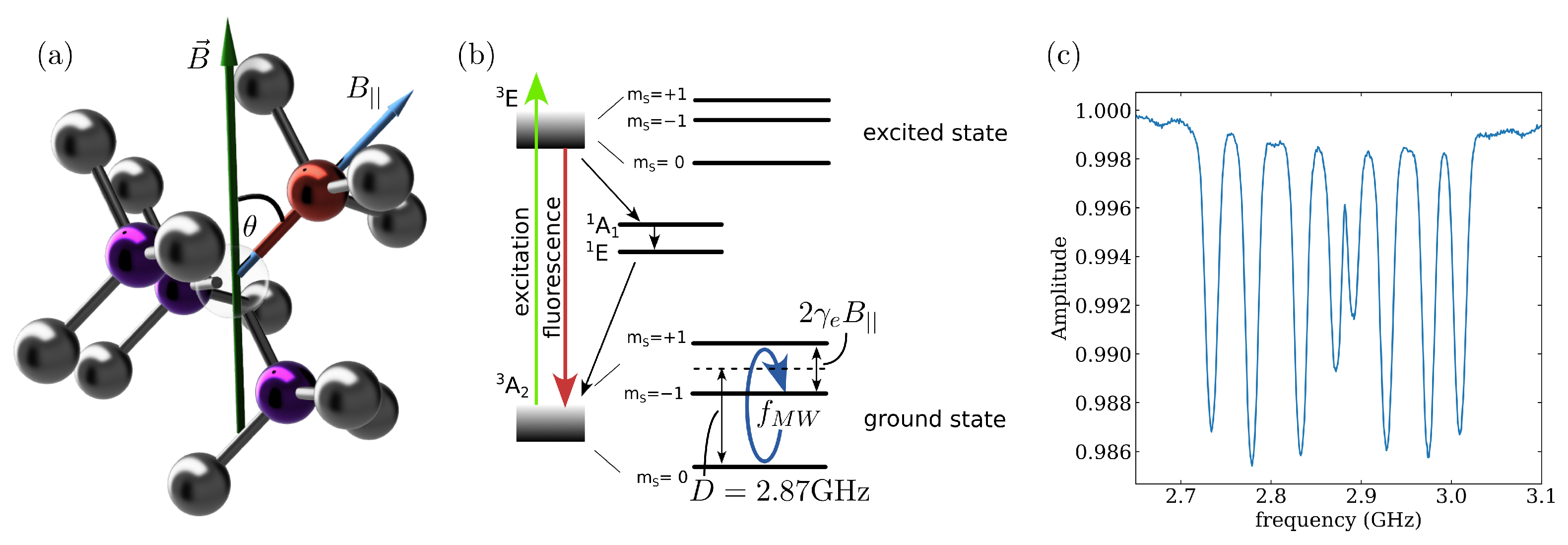
An NV center is a point defect in a diamond in which two carbon atoms are replaced by a nitrogen atom (red) and an adjacent vacancy (Figure 1a). NV centers in a diamond can have four orientations within its tetrahedral structure (purple atoms). The negatively charged NV center is a spin system with spin triplets in ground (3) and excited states (3) (see Figure 1b). The optical excitation of the ground state is spin-preserving. An state fluoresces at as it decays. However, the state tends towards non-radiative transitions to the 1 singlet state, making the spin state optically detectable. Microwave magnetic fields resonant to electron spin transitions in the 3 ground state therefore reduce the NV center’s fluorescence and could be used to detect spin states.

Figure 1.
(a) Diamond crystal structure formed by carbon atoms (gray), with a nitrogen atom (red) and adjacent vacancy forming a nitrogen vacancy (NV) center. NV centers are formed in all axes of the diamond lattice (indicated by purple-colored carbon atoms). The green arrow indicates an external magnetic field , whereas the blue arrow indicates the vectorial projection on the NV-axis . (b) Simplified energy diagram of the NV center. A continuous sweep of leads to the ground state being flipped from to at different frequencies due to the different components. This spin can be detected optically, as pumping with green light is spin-preserving and decay via a singlet state with fluorescence in the infrared range is more likely. (c) An example spectrum containing eight fluorescence dips caused by different components for each NV center axis and, therefore, different Zeeman splittings . From the different-frequency deltas between these dips, the might be calculated. Figure based on [16].
The magnetic sensing capability of the NV center is due to the interaction of an external magnetic field (the green arrow in Figure 1a) with the electron spin, causing a Zeeman shift in the states that is visible in ODMR measurements. In the absence of an applied magnetic field, zero-field splitting (ZFS) is observed due to internal crystal strain. The ZFS center frequency ( at room temperature) also shifts with temperature [9,17], which allows for simultaneous magnetic field and temperature sensing.
For NV ensembles aligned along four crystal axes, sweeping the microwave frequency while observing the fluorescence yields eight dips, corresponding to the and levels, for each of the four NV axes (see Figure 1c).
As high-sensitivity magnetic field sensors, NV-center-based applications have already been used as current sensors [18,19,20,21], reaching dynamic ranges up to with a step size of [18]. However, these and other setups are often quite complex and not really portable. Here, we propose a quantum current sensor with all electrical inputs and outputs in a compact form.
2. Materials and Methods
2.1. Measurement Setup
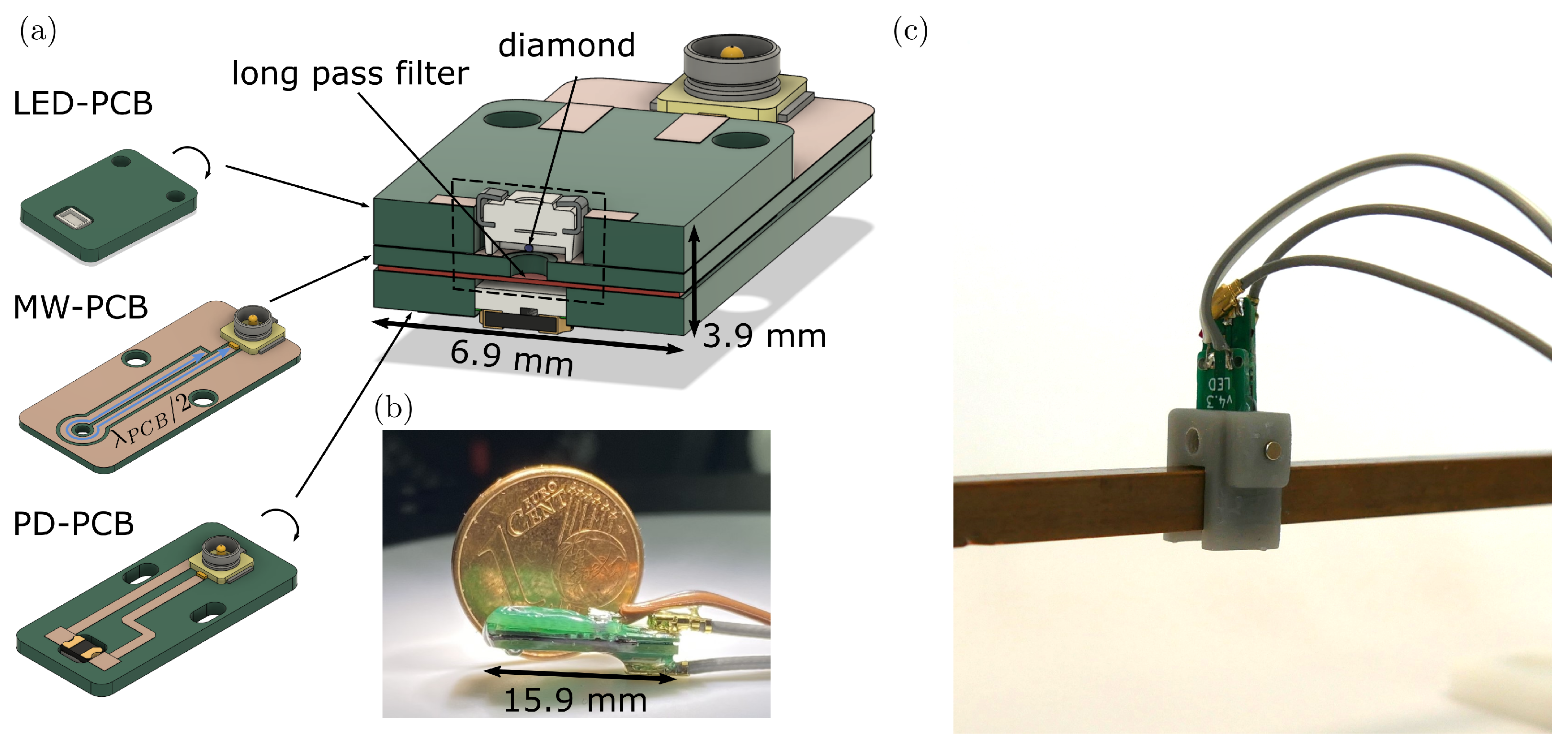
The sensor is designed as described in detail in a previous publication [16]. Its setup is shown in Figure 2a. Basically, the sensor consists of three stacked printed circuit boards (PCBs) that emulate the basic principles of an optical quantum sensor based on NV centers. The LED-PCB contains an LED as the pump light source. The 150 diamond is attached to the LED with an optical adhesive. Microwave excitation is provided by a microwave antenna located on the microwave PCB (MW-PCB). The resulting fluorescence in the red region is formed by a filter foil between the MW-PCB and the photodiode PCB (PD-PCB). The PD-PCB contains the photodiode that converts the fluorescence into a current signal. A clip to hold the sensor and integrate the offset magnet is printed using stereolithography (SLA). Microwave signals are swept using a vector signal generator (SMBV100B, Rhode & Schwarz, Munich, Germany). The LED current is supplied by a lab-built current source powered by a block battery. The photodiode current is amplified by a lab-built [22] transimpedance amplifier (TIA) and measured with a multimeter (GDM9061, GW-Instek, Taipeh, Taiwan).
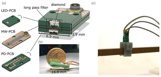
Figure 2.
(a) Sensor setup with LED-PCB, MW-PCB, filterfoil, and PD-PCB, (b) photo of the integrated quantum sensor, and (c) sensor integrated into 3D printed clip. An offset magnet is integrated into the clip as well.
2.2. Simulation of Magnetic Field Distribution
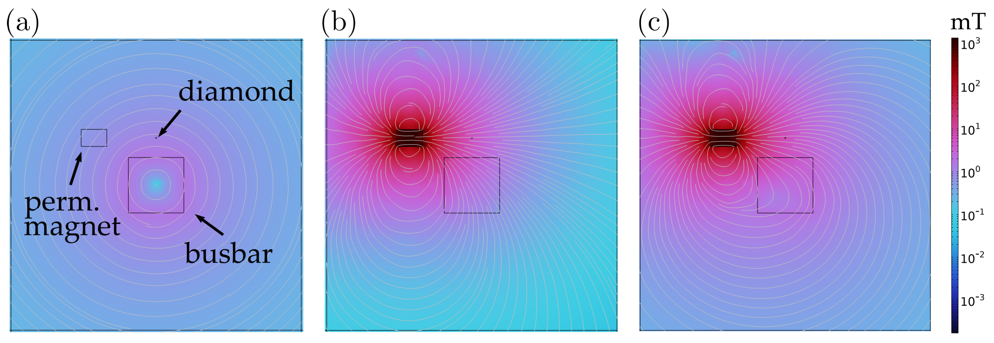
The calculation of magnetic fields around conductors that are not round and therefore do not follow the simplified formulas of Biot–Savart is not trivial. Hence, a numerical approach is chosen and the field distribution is simulated numerically. COMSOL Multiphysics 6.1 is a simulation software for modeling and analyzing complex physical systems. In this study, COMSOL is used to create a three-dimensional model of the measurement setup. The busbar is modeled as a piece of copper. A current of 0–30 is applied via the coil feature of the magnetic field physics module in COMSOL. The diamond is approximated as a sphere of 150 and is located above the center of the busbar. The measurement comes from the fact that the diamond is located from the nearest edge. A thick insulation layer was taken into account during printing. Additionally, a cylindrical permanent magnet with a diameter of and a height of was simulated. The material is labeled by the manufacturer as NdFeB, with a magnetization of N45. This magnet is positioned at the height of the diamond and shifted to one side by . Simulations are performed without an activated magnet and with currents between 0–30 . The maximum average volume in the diamond sphere is at (see Figure 3a). The magnet produces a theoretical magnetic field of (see Figure 3b). The current and the offset magnetic field are then applied together (see Figure 3c). The uniformity of the resulting magnetic field in the x-direction, i.e., the axis on which the diamond and the offset magnet are aligned, is given by the angle and is calculated as

Figure 3.
(a) Magnetic field distribution at without a permanent magnet. (b) Magnetic field distribution with a permanent magnet N45 (sintered NdFeB) and without current. (c) Magnetic field distribution at 30A together with a permanent magnet, showing a superimposed magnetic field distribution.
Averaged over the volume, a homogeneous field with an average deviation of from the x-axis is found. This setup would therefore be suitable for measurements using one axis of the NV center, which allows high sampling rates that are easy to obtain. For this DC application, however, a complete sweep of all NV axes is used.
2.3. Extraction of Magnetic Field Information from ODMR Measuremnts
To extract the information of the external magnetic field, the procedure described in [23] is used. The first eight superimposed Lorenz functions, such as
are fitted to a spectrum where C is the ODMR contrast, and are the eight resonance frequencies, and is the full width at half maximum (FWHM) of the resonance dips.
Now an attempt is made to fit a B-field vector that would produce exactly these resonance frequencies. To do this, a matrix is defined that represents the structure of the NV center as unit vectors in the crystal structure and follows from the trahedral arrangement of the crystal lattice:
As described in the introduction, an external magnetic field projects on to the axis of the NV center, resulting in a parallel and a perpendicular component, and , for each axis. As described in [24], this results in specific resonance frequencies
with as
Here, D is the zero-field splitting parameter which allows us to obtain information about the crystal temperature [9], is the gyromagnetic ratio, and E is the crystal strain parameter.
With a spherical magnetic field vector , a fit function is defined that optimizes , and D so that the measured resonances fit the ones calculated using Equation (4). Thus, it is possible to extract the absolute magnetic field if the orientation of the diamond is known the direction of the vector can also be determined. In the present application, this is not necessary, and the measurement can be performed with randomly oriented diamonds.
3. Results and Discussion
The magnetic fields are measured in 3 A increments. A frequency sweep is performed between 2.6 and 3.1 GHz. The LED in the sensor head is driven with a constant current of . The output of the TIA is measured with a multimeter. The spectra of the different busbar currents are shown in Figure 4a.
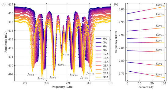
Figure 4.
(a) The resulting spectra measured with the sensor setup. The current is varied between 0 and . The resulting output of the TIA is shown in milivolts as a function of the frequency sweep. The resonance frequencies of the individual NV axes are labeled with . (b) The extracted resonance frequencies shift with increasing busbar current. Characteristic non-linearities can be recognized at higher fields.
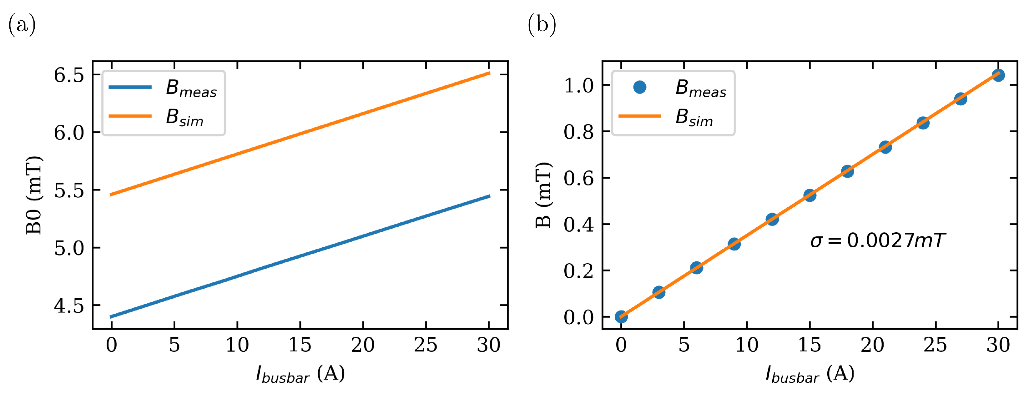
A comparison between the resulting measurements and the simulated values is shown in Figure 5a. The constant offset is measured as , which is slightly different from the simulated value of . By compensating for the offset, the slope of the simulation and the measurement fit, with a standard deviation of (see Figure 5b).
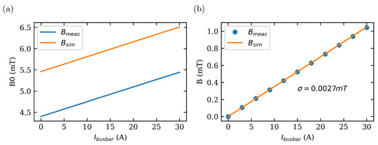
Figure 5.
(a) Measured and simulated absolute magnetic field B. (b) Measured and simulated magnetic field without offset.
The values obtained with the magnetic field-based current sensor indicate that the current may be measured with a fully linear slope of and a current value standard deviation of . With respect to the measurement range, this results in an accuracy of . The measuring range of 0–30 was selected due to the availability of a current source with this current capacity. The mean absolute error
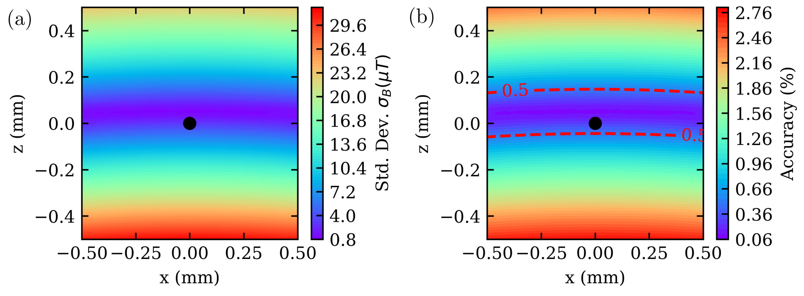
is calculated as . If converted into a current value by the simulated slope, this would result in a mean absolute error for the current values of . The current method is predicated upon a precise interplay between the simulation and the positioning accuracy of the sensor. The measurement data are then compared with the simulation data in which the diamond is moved relative to the current simulated position. The permanent magnet is disregarded, and only the gradient resulting from the current is analyzed. Consequently, the simulation can be conducted in two dimensions, as no alterations are anticipated in the y-direction, which represents the axis of the busbar. An area of (1 × 1) mm2 with a resolution of is selected on each axis. Figure 6a illustrates the correlation between the standard deviation of the simulated and measured values. On both graphs, a black dot indicates the initial simulation location based on the production data of the sensor and clip. It is evident that the sensor is in a satisfactory position for integrating measurement and simulation data; however, it is not optimally positioned to achieve the best possible result. This discrepancy may be attributed to the diamond’s non-central positioning with respect to the LED, resulting in a slight deviation from the assumed position or, alternatively, the sensor’s suboptimal placement within the holder. The accuracy of the sensor in the measuring range 0–30 in relation to the position of the diamond is shown in Figure 6b. In order to achieve an accuracy of 0.5%, the diamond must be positioned in an almost horizontal band, at a height of 160 , and in the center.
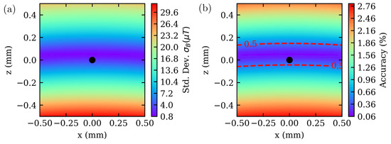
Figure 6.
(a) Spatial change in standard deviation between the measured and simulated magnetic fields. Marked in black is the position of the sensor which was used for the simulation and which is based on the production data of the sensor and the clip. (b) Measured and simulated magnetic field without offset.
Regarding the general measurement range, the NV center, and therefore the sensing technique, is not the limiting factor. Only from about a external field do the excited and ground state overlap, rendering the extraction of the resonance frequencies no longer easily possible. If an additional magnetic field of caused by the current is added to the existing offset, the measuring range is already 0–600 . The previously described fitting process also includes the ZFS parameter D, which is mainly caused by a change in temperature of the diamond. The sensor should therefore be able to function and measure magnetic fields correctly even when the temperature changes. The non-linear shift of the resonances due to off-axis magnetic fields is also covered by the parameter . Therefore, we assume that the accuracy of the current sensor might be in a 0–600 range and even lower in higher measurement ranges. However, this is a very theoretical consideration, as the conductor rail would have to be changed for this load and the field distribution would have to be recalculated. According to tables given in DIN 43 671, a load of for the used busbar, which has a cross-section of , can be assumed even without a correction factor for an increased accepted temperature. In this range, the sensor could be used with an accuracy of . These results underscore the potential of the sensor for high-precision current measurements in practical applications, contingent upon the adaptation of its physical and magnetic configurations to support the desired current ranges. Moreover, a workflow was presented that demonstrates highly accurate measurements in practical applications using only numerical simulation results. Additionally, it was demonstrated that the accuracy of the measurements can be enhanced through the implementation of a reference measurement and the adjustment of the simulation parameters. This workflow can be further utilized when measuring currents in high-current applications such as DC supply cables using quantum sensors without contact.
Author Contributions
Conceptualization and sensor design, J.P.; methodology, J.P. and J.H.; validation, J.P., L.H. and J.H.; formal analysis, J.P. and A.-S.B.; investigation, J.P. and L.H.; resources, J.P.; data curation, J.P., F.H. and J.H.; writing—original draft preparation, J.P.; writing—review and editing, L.H., D.S., J.H., A.-S.B., F.H., M.G. and P.G.; visualization, J.P.; supervision, M.G. and P.G.; project administration, P.G.; funding acquisition, M.G. and P.G. All authors have read and agreed to the published version of the manuscript.
Funding
This research was funded by Bundesministerium für Bildung und Forschung (13N15971 and 13N15489).
Institutional Review Board Statement
Not applicable.
Informed Consent Statement
Not applicable.
Data Availability Statement
The data underlying the results presented in this paper are not publicly available at this time but may be obtained from the authors upon reasonable request.
Acknowledgments
The authors would like to thank the members of the projects OCQNV, Quantum IRES, RaQuEl, and O3Q for their helpful discussions, as well as the Research Center for Information and Communications Technologies of the University of Granada (CITIC−UGR) for a constructive exchange.
Conflicts of Interest
The authors declare no conflicts of interest. The funders had no role in the design of the study; in the collection, analyses, or interpretation of data; in the writing of the manuscript; or in the decision to publish the results.
Abbreviations
The following abbreviations are used in this manuscript:
| NV | Nitrogen vacancy |
| LED | Light emmitig diode |
| DC | Direct current |
| ODMR | Optical detected magnetic resonance |
| ZFS | Zero field splitting |
| PCB | Printed circuit board |
| MW | Microwave |
| PD | Photodiode |
| SLA | Stereolithography |
| TIA | transimpedance amplifier |
| FWHM | Full width half maximum |
References
- Stürner, F.M.; Brenneis, A.; Buck, T.; Kassel, J.; Rölver, R.; Fuchs, T.; Savitsky, A.; Suter, D.; Grimmel, J.; Hengesbach, S.; et al. Integrated and Portable Magnetometer Based on Nitrogen-Vacancy Ensembles in Diamond. Adv. Quantum Technol. 2021, 4, 2000111. [Google Scholar] [CrossRef]
- Xie, Y.; Yu, H.; Zhu, Y.; Qin, X.; Rong, X.; Duan, C.K.; Du, J. A hybrid magnetometer towards femtotesla sensitivity under ambient conditions. Sci. Bull. 2021, 66, 127–132. [Google Scholar] [CrossRef] [PubMed]
- Silani, Y.; Smits, J.; Fescenko, I.; Malone, M.W.; McDowell, A.F.; Jarmola, A.; Kehayias, P.; Richards, B.A.; Mosavian, N.; Ristoff, N.; et al. Nuclear quadrupole resonance spectroscopy with a femtotesla diamond magnetometer. Sci. Adv. 2023, 9, eadh3189. [Google Scholar] [CrossRef]
- Zhou, T.X.; Stöhr, R.J.; Yacoby, A. Scanning diamond NV center probes compatible with conventional AFM technology. Appl. Phys. Lett. 2017, 111, 163106. [Google Scholar] [CrossRef]
- Rondin, L.; Tetienne, J.P.; Spinicelli, P.; Savio, C.D.; Karrai, K.; Dantelle, G.; Thiaville, A.; Rohart, S.; Roch, J.F.; Jacques, V. Nanoscale magnetic field mapping with a single spin scanning probe magnetometer. Appl. Phys. Lett. 2012, 100. [Google Scholar] [CrossRef]
- Hong, S.; Grinolds, M.S.; Pham, L.M.; Sage, D.L.; Luan, L.; Walsworth, R.L.; Yacoby, A. Nanoscale magnetometry with NV centers in diamond. Mrs Bull. 2013, 38, 155–161. [Google Scholar] [CrossRef]
- Balasubramanian, G.; Chan, I.Y.; Kolesov, R.; Al-Hmoud, M.; Tisler, J.; Shin, C.; Kim, C.; Wojcik, A.; Hemmer, P.R.; Krueger, A.; et al. Nanoscale imaging magnetometry with diamond spins under ambient conditions. Nature 2008, 455, 648–651. [Google Scholar] [CrossRef]
- Zhang, C.; Shagieva, F.; Widmann, M.; Kübler, M.; Vorobyov, V.; Kapitanova, P.; Nenasheva, E.; Corkill, R.; Rhrle, O.; Nakamura, K.; et al. Diamond Magnetometry and Gradiometry Towards Subpicotesla dc Field Measurement. Phys. Rev. Appl. 2021, 15, 064075. [Google Scholar] [CrossRef]
- Acosta, V.M.; Bauch, E.; Ledbetter, M.P.; Waxman, A.; Bouchard, L.S.; Budker, D. Temperature Dependence of the Nitrogen-Vacancy Magnetic Resonance in Diamond. Phys. Rev. Lett. 2010, 104, 070801. [Google Scholar] [CrossRef] [PubMed]
- Neumann, P.; Jakobi, I.; Dolde, F.; Burk, C.; Reuter, R.; Waldherr, G.; Honert, J.; Wolf, T.; Brunner, A.; Shim, J.H.; et al. High-Precision Nanoscale Temperature Sensing Using Single Defects in Diamond. Nano Lett. 2013, 13, 2738–2742. [Google Scholar] [CrossRef]
- Abrahams, G.J.; Ellul, E.; Robertson, I.O.; Khalid, A.; Greentree, A.D.; Gibson, B.C.; Tetienne, J.P. Handheld Device for Noncontact Thermometry via Optically Detected Magnetic Resonance of Proximate Diamond Sensors. Phys. Rev. Appl. 2023, 19, 054076. [Google Scholar] [CrossRef]
- Xu, R.; Zhang, Z.; Du, B.; Zhang, Y.; Huang, K.; Cheng, L. Ultra-Sensitive Two-Dimensional Integrated Quantum Thermometer Module Based on the Optical Detection of Magnetic Resonance Using Nitrogen-Vacancy Centers. IEEE Sens. J. 2022, 22, 15316–15322. [Google Scholar] [CrossRef]
- Dolde, F.; Fedder, H.; Doherty, M.W.; Nöbauer, T.; Rempp, F.; Balasubramanian, G.; Wolf, T.; Reinhard, F.; Hollenberg, L.C.L.; Jelezko, F.; et al. Electric-field sensing using single diamond spins. Nat. Phys. 2011, 7, 459–463. [Google Scholar] [CrossRef]
- Pezzagna, S.; Meijer, J. Quantum computer based on color centers in diamond. Appl. Phys. Rev. 2021, 8, 011308. [Google Scholar] [CrossRef]
- Kennedy, T.; Charnock, F.; Colton, J.; Butler, J.; Linares, R.; Doering, P. Single-Qubit Operations with the Nitrogen-Vacancy Center in Diamond. Phys. Status Solidi (B) 2002, 233, 416–426. [Google Scholar] [CrossRef]
- Pogorzelski, J.; Horsthemke, L.; Homrighausen, J.; Stiegekötter, D.; Gregor, M.; Glösekötter, P. Compact and Fully Integrated LED Quantum Sensor Based on NV Centers in Diamond. Sensors 2024, 24, 743. [Google Scholar] [CrossRef] [PubMed]
- Fujiwara, M.; Sun, S.; Dohms, A.; Nishimura, Y.; Suto, K.; Takezawa, Y.; Oshimi, K.; Zhao, L.; Sadzak, N.; Umehara, Y.; et al. Real-time nanodiamond thermometry probing in vivo thermogenic responses. Sci. Adv. 2020, 37, eaba9636. [Google Scholar] [CrossRef]
- Hatano, Y.; Shin, J.; Tanigawa, J.; Shigenobu, Y.; Nakazono, A.; Sekiguchi, T.; Onoda, S.; Ohshima, T.; Arai, K.; Iwasaki, T.; et al. High-precision robust monitoring of charge/discharge current over a wide dynamic range for electric vehicle batteries using diamond quantum sensors. Sci. Rep. 2022, 12, 13991. [Google Scholar] [CrossRef] [PubMed]
- Liu, Q.; Xie, F.; Peng, X.; Hu, Y.; Wang, N.; Zhang, Y.; Wang, Y.; Li, L.; Chen, H.; Cheng, J.; et al. Millimeter-Scale Temperature Self-Calibrated Diamond-Based Quantum Sensor for High-Precision Current Sensing. Adv. Quantum Technol. 2023, 6, 2300210. [Google Scholar] [CrossRef]
- Kubota, K.; Hatano, Y.; Kainuma, Y.; Shin, J.; Nishitani, D.; Shinei, C.; Taniguchi, T.; Teraji, T.; Onoda, S.; Ohshima, T.; et al. Wide temperature operation of diamond quantum sensor for electric vehicle battery monitoring. Diam. Relat. Mater. 2023, 135, 109853. [Google Scholar] [CrossRef]
- Zhao, L.; Wang, L.; Sun, F.; Xu, K.; Wang, X.; Wang, Y. Design of Current Sensor based on Quantum Precision Measurement. In Proceedings of the 2020 11th International Conference on Prognostics and System Health Management (PHM-2020 Jinan), Jinan, China, 23–25 October 2020; IEEE: Piscataway, NJ, USA, 2020. [Google Scholar] [CrossRef]
- Homrighausen, J.; Horsthemke, L.; Pogorzelski, J.; Trinschek, S.; Glösekötter, P.; Gregor, M. Edge-Machine-Learning-Assisted Robust Magnetometer Based on Randomly Oriented NV-Ensembles in Diamond. Sensors 2023, 23, 1119. [Google Scholar] [CrossRef] [PubMed]
- Homrighausen, J.; Hoffmann, F.; Pogorzelski, J.; Glösekötter, P.; Gregor, M. Microscale Fiber-Integrated Vector Magnetometer with On-Tip Field Biasing using NV Ensembles in Diamond Microcystals. arXiv 2024, arXiv:2404.14089. [Google Scholar] [CrossRef]
- Doherty, M.W.; Dolde, F.; Fedder, H.; Jelezko, F.; Wrachtrup, J.; Manson, N.B.; Hollenberg, L.C.L. Theory of the ground-state spin of the NV- center in diamond. Phys. Rev. B 2012, 85, 205203. [Google Scholar] [CrossRef]

Disclaimer/Publisher’s Note: The statements, opinions and data contained in all publications are solely those of the individual author(s) and contributor(s) and not of MDPI and/or the editor(s). MDPI and/or the editor(s) disclaim responsibility for any injury to people or property resulting from any ideas, methods, instructions or products referred to in the content. |
© 2024 by the authors. Licensee MDPI, Basel, Switzerland. This article is an open access article distributed under the terms and conditions of the Creative Commons Attribution (CC BY) license (https://creativecommons.org/licenses/by/4.0/).