Abstract
Passive wireless sensing systems, particularly passive antenna sensors, offer a viable alternative to traditional wired and active sensors for long-term structural health monitoring due to their simplicity, easy installation and maintenance, and ability to measure strain without an external power supply. Customization of antenna shape can also adapt to various structural geometries. However, sensor fabrication using chemical etching is expensive and time-consuming, which is unsuitable for limited-quantity production. To address this, this study explores the potential of extrusion-based additive manufacturing to produce cost-effective passive wireless antenna strain sensors. The study investigates polylactic acid’s mechanical and electromagnetic properties for substrate design and uses multi-physics simulation to estimate strain-sensing performance. The obtained results show similar strain-sensing performance to sensors produced through chemical etching, making the manufacturing process a promising alternative.
1. Introduction
Structural health monitoring (SHM) is the study of monitoring an engineered structure’s safety over time by taking periodic measurements such as strain, displacement, acceleration, humidity, and temperature. The goal is to accurately detect any problems that could impact the structure’s reliability and life cycle [1]. Strain is a critical measurement that represents stress concentration and could lead to crack development during service. Wireless sensors are commonly used for SHM, but they require a power source for operating systems. Eventually, the system requires expensive periodic battery replacement, data acquisition, which increases installation time and cost due to cable connectors [2].
To reduce periodic upkeep of the battery system, a passive wireless communication sensor was created. Antenna strain sensors enable long-term measurement without the need for a power source on the sensor side [3]. Previous research attempts and efforts in development of antenna strain sensors that satisfy SHM requirements has been an area of continuing research [4]. However, in these preceding studies, the cost of the antenna sensors relied on the expensive and relatively time-consuming chemical etching process. We propose the use of additive manufacturing (AM) as an alternative to fabricating antenna strain sensors. AM is the method of constructing three-dimensional objects by layering materials according to a computer-aided design (CAD). This technology has proven itself to be an asset to a wide range of fields due to its efficiency, flexibility, and cost-effectiveness compared to traditional subtractive manufacturing techniques [5]. Through Production 3D printing, multiple iterations and functional end-use small-production quantities are possible at a fraction of the cost [6].
2. Method
2.1. Strain Sensing Mechanism of the Antenna Sensor
The passive communication device used in this study was the Ultra High Frequency (UHF) gen 2 standard, which allows for a broad frequency range of 840 to 960 MHz. This standard utilizes the Tagformance Pro© radio frequency identification (RFID) reader (Voyantic, Seattle, WA, USA), which emits an electromagnetic interrogation signal that powers up the receiving antenna sensor, as illustrated in Figure 1a.

Figure 1.
Strain sensing mechanism of antenna sensors: (a) Schematic of a passive (battery free) wireless system; (b) Strain sensing.
The antenna sensor consists of three layers: (1) microstrip with a metallic pattern aiming for high radiation performance, (2) substrate to separate the microstrip patch and ground plan allowing an electromagnetic field to generate, and (3) a ground plan which is not designed as part of this study. The emitted signal is received by the antenna sensor, which captures a portion of the power and transfers it to the Radio Frequency Identification (RFID) transponder chip. If the transferred power is higher than the activation power threshold of the chip, it is activated. In this state, the chip modulates the return signal in the form of a backscattered signal, which is then received by the reader. This backscattered signal contains information about the strain level of the sensor.
The resonance frequency of a patch antenna with a different strain level is determined as shown in Equation (1):
where is the speed of the light, is the physical length of the patch antenna, is the effective dielectric constant of the antenna substrate, is the additional electrical length due to the fringing effect, and is an applied strain level.
As shown in Figure 1b, the backscattered signal output forms interrogation curves, where the minimum point of the interrogation curve indicates the resonance frequency of the antenna sensor. As shown in Figure 1b, under tensile strain, the resonance frequency of the antenna sensor will decrease and increase when experiencing compressive strain.
2.2. Design of Substrate and Patch Antenna
Material properties are key components when designing antenna sensors. Under the proposed AM fabrication method, the mechanical and electromagnetic properties were tested to gauge the impact of the anisotropic behavior inherent in AM printing technology; this remains a primary concern for end-use printing [6]. The anisotropic behavior is governed by the interlayer bond of the microstructure latices created during the layering process while printing. The A2200 3D Multi-Material Electronics Printer© (nano3Dprint, Burlingame, CA, USA) was used to fabricate the sensor and substrate using a concurrent printing technique. The substrate was printed in polylactic acid (PLA), while the metal pattern of the patch antenna was printed in silver nano ink which had a conductivity of 2 Ω/cm.
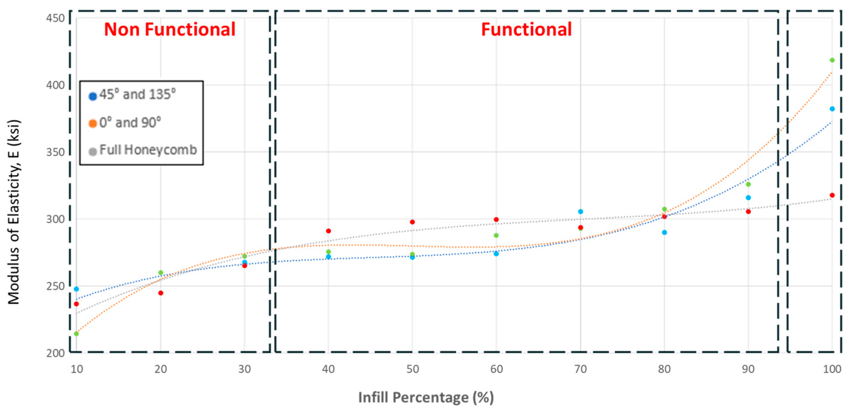
A preliminary material study of the extrusion-based 3D printing process was conducted, following ASTM D638-14 on the 810 Material Test System. Two Rectilinear ( and Full Honeycomb (FHC) patterns were compared as a function of their infill density. The three features that impacted the final material behavior and strength were: layer height, layer density, and printing direction. The stress–strain constitutive relation, shown in Figure 2, was found to be dependent on the infill density, print orientation, and pattern with relation to the tensile loading condition.
Figure 2.
Print pattern’s infill comparison for modulus of elasticity (E).
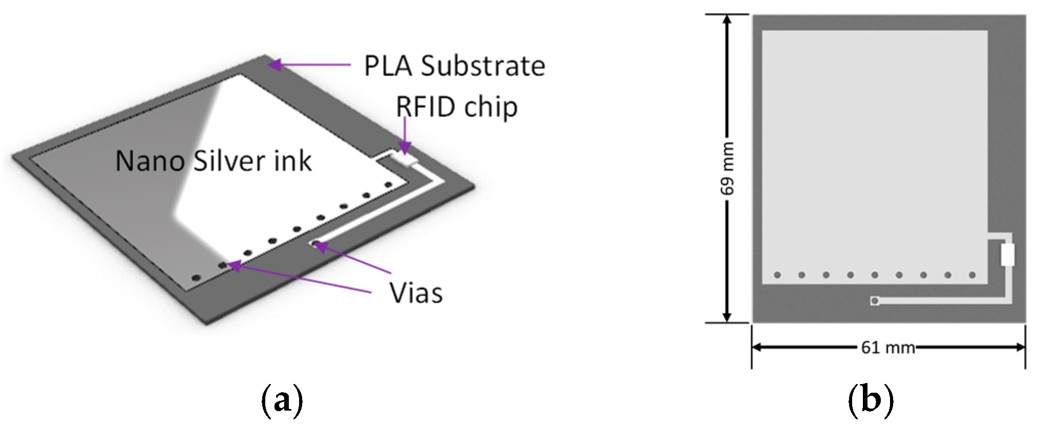
The prototype for the patch antenna was created by building on previous research that utilized a folded-patch topology for the antenna, which can be found in our previous study [7,8]. To construct the antenna, conductive silver nano ink was used to 3D print it onto a PLA substrate. To make the antenna smaller, the antenna and ground plane were connected with vias. In addition, the RFID chip MONZA R6-P (IMPINJ, Seattle, WA, United States of America) was used in the study to prevent data collision. The final dimensions of the printed antenna sensor were determined through an iterative process, where the team experimented with different dimensions and adjusted until they found the optimal size. The resulting dimensions of the antenna sensor were 61 mm in width, 69 mm in length, and 1 mm in thickness, as illustrated in Figure 3.
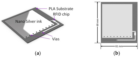
Figure 3.
Initial design of a patch antenna sensor: (a) perspective view (b) plan view.
3. Results
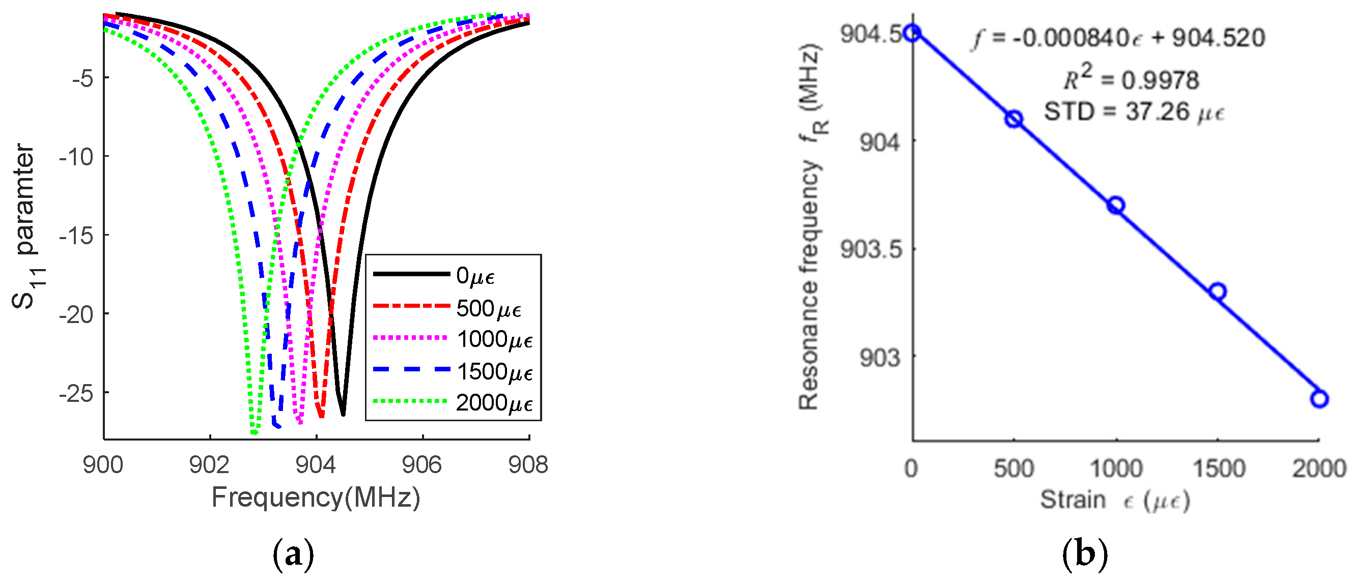
To accurately describe the antenna sensor’s electromagnetic behavior under strain, we must consider two coupled physical domains, mechanics and electromagnetics. The coupled multi-physics simulation requires mechanical simulations to determine the deformed shape of the antenna, and then estimate electromagnetic response. Detail modeling techniques and procedures are referred to in our previous study [9]. As shown in Figure 4a, scattering parameter (S11) is simulated with different strain levels. Applied strain is up to 2000 with the step size of 500 To estimate the strain sensitivity, we extract the minimum values of S11, and perform a linear regression as shown in Figure 4a. The obtained strain sensitivity is −840 and the coefficient of determination is 0.9978.
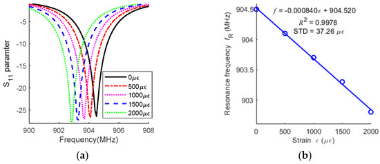
Figure 4.
Simulation strain sensitivity of the optimized sensor: (a) S11 scattering parameter; (b) strain vs. frequency plot.
4. Discussion & Summary
In this study, we delved into the various possibilities that 3D printing techniques present in the creation of antenna sensors. We found the details by carrying out extensive mechanical analyses on PLA, with the aim of establishing the elastic modulus in relation to the different infill densities. Additionally, we utilized multi-physics simulation to obtain precise estimations of strain sensing, and from our findings, we were able to conclude that the AM process has immense potential for producing antenna sensors. Our investigation produced a strain sensitivity of −840 με/Hz, and we observed a good linearity in the coefficient of determination of 0.9978. Consequently, we believe that 3D printing technology can be harnessed to fabricate antenna sensors.
As a follow-up study, we intend to carry out nonlinear and fatigue tests to obtain more detailed insights into the mechanical properties of PLA. Furthermore, we plan to develop a method to improve conductivity of a nano ink. Ultimately, a more systematic approach to antenna sensor design and 3D printing will be required to maximize the strain sensing and wireless interrogation distance.
Author Contributions
Conceptualization, S.-H.J., S.-H.N. and C.C.; methodology, J.D., S.-H.J., S.-H.N. and C.C. software, J.D., X.S. and C.C.; validation, J.D. and X.S. formal analysis, J.D., X.S., S.-H.J., S.-H.N. and C.C.; investigation, J.D.; resources, J.D. and C.C.; data curation, J.D. and X.S.; writing—original draft preparation, J.D.; writing—review and editing, C.C.; visualization, J.D. and C.C.; supervision, C.C.; project administration, C.C.; funding acquisition, C.C. All authors have read and agreed to the published version of the manuscript.
Funding
The work was supported by the ATC+ Program (20014127, Development of a smart monitoring system integrating 3D printed battery-free antenna sensor technology with AI optimization) funded by the Ministry of Trade, Industry & Energy (MOTIE, Republic of Korea).
Data Availability Statement
The data presented in this study are available upon request.
Conflicts of Interest
The authors declare no conflict of interest.
References
- Lynch, J.P.; Loh, K.J. A summary review of wireless sensors and sensor networks for structural health monitoring. Shock. Vib. Dig. 2006, 38, 91–128. [Google Scholar] [CrossRef]
- Abdulkarem, M.; Samsudin, K.; Rokhani, F.Z.; Rasid, M.F.A. Wireless sensor network for structural health monitoring: A contemporary review of technologies, challenges, and future Direction. Struct. Health Monit. 2020, 19, 693–735. [Google Scholar] [CrossRef]
- Yi, X.; Cho, C.; Cook, B.; Wang, Y.; Tentzeris, M.M.; Leon, R.T. A slotted patch antenna for wireless strain sensing. In Proceedings of the ASCE 2014 Structures Congress, Boston, MA, USA, 3–5 April 2014. [Google Scholar]
- Deivasigamani, A.; Daliri, A.; Wang, C.; John, S. A review of passive wireless sensors for structural health monitoring. Mod. Appl. Sci. 2013, 7, 57–76. [Google Scholar] [CrossRef]
- Zhang, J.; Tian, G.Y.; Marindra, A.M.; Sunny, A.; Zhao, A.B. A Review of Passive RFID Tag Antenna-Based Sensors and Systems for Structural Health Monitoring Applications. Sensors 2017, 17, 265. [Google Scholar] [CrossRef] [PubMed]
- Somireddy, M.; Czekanski, A. Anisotropic material behavior of 3D printed composite structures—Material extrusion additive manufacturing. Mater. Des. 2020, 195, 108953. [Google Scholar] [CrossRef]
- Yi, X.; Cho, C.; Cooper, J.; Wang, Y.; Tentzeris, M.M.; Leon, R.T. Passive wireless antenna sensor for strain and crack sensing—Electromagnetic modeling, simulation, and testing. Smart Mater. Struct. 2013, 22, 085009. [Google Scholar] [CrossRef]
- Finkenzeller, K. RFID Handbook, 2nd ed.; John Wiley & Sons: New York, NY, USA, 2003. [Google Scholar]
- Cho, C.; Long, L.; Park, J.; Jang, S.-H. A multi-physics informed antenna sensor model through the deep neural network regression. Smart Struct. Syst. 2021, 28, 335–362. [Google Scholar]
Disclaimer/Publisher’s Note: The statements, opinions and data contained in all publications are solely those of the individual author(s) and contributor(s) and not of MDPI and/or the editor(s). MDPI and/or the editor(s) disclaim responsibility for any injury to people or property resulting from any ideas, methods, instructions or products referred to in the content. |
© 2023 by the authors. Licensee MDPI, Basel, Switzerland. This article is an open access article distributed under the terms and conditions of the Creative Commons Attribution (CC BY) license (https://creativecommons.org/licenses/by/4.0/).


