Proceeding Paper

Functional Converter for Intelligent Sensor and Its Layout Design †

1
Department of Computer Science and Engineering, Saint Petersburg Electrotechnical University LETI, 197022 St. Petersburg, Russia
2
Department of Telecommunication Systems, Ufa State Aviation Technical University, Ufa, 450008 The Republic of Bashkortostan, Russia
*
Author to whom correspondence should be addressed.
Presented at the 15th International Conference “Intelligent Systems” (INTELS’22), Moscow, Russia, 14–16 December 2022.
Eng. Proc. 2023, 33(1), 50; https://doi.org/10.3390/engproc2023033050
Published: 17 July 2023
(This article belongs to the Proceedings of 15th International Conference “Intelligent Systems” (INTELS’22))

Abstract

:
Recently, the number of cyber-physical systems and systems with embedded sensors has been increasing. In order to minimize the amount of information transmitted, a new paradigm is being developed that involves moving data processing as close as possible to the point of its generation. At the same time, there is a need to create devices that will provide computations near the sensors. The article considers an approach to the primary processing of a quasi-digital sensor signal. The authors show a variant of the organization of calculations in pulse form, based on the method of small increments. The method is focused on the usage of simple logical elements with the realization of a transfer function in the base of increment/decrement operations. The solution proposed by the authors is effective in terms of simplicity of hardware implementation and can be used to connect sensors with pulse output to digital processing systems. The considered circuit solutions can be used for the implementation in programmable logic device of different levels of complexity, as well as for the manufacture of the transducer in the form of a custom circuit.

1. Introduction

Recently, the number of cyber-physical systems and systems with embedded sensors is increasing. This leads to an increased load on the means of communication between such systems. To minimize the amount of information transferred, a new paradigm of edge computing is being developed. It implies moving data processing as close as possible to the point where it is received [1,2]. In the context of this paradigm, there is a need to develop special devices that provide computations near sensors. These should be compact, energy-efficient and fault-tolerant modules, which can be manufactured as separate chips or integrated with sensing elements in a single chip [3,4]. Hardware implementation of simple functional signal conversions is available in analog, digital, pulse, and mixed formats. Obviously, performing calculations in the formats of signals obtained at the outputs of sensitive elements will allow us to avoid additional operations related to format conversions. Sensors often generate a frequency output signal [5,6]. Also, analog-to-frequency converters can be installed in chips of sensors with an analog output [7,8]. The frequency output signal can be represented as a stream of pulses [9] or pulse-width modulated (PWM) signals [10]. In a pulse stream, the carrier of information is the number of pulses per unit time. In a PWM signal, the information is associated with the relative duration of the pulses. In both cases, the amplitude of the signals is the same and can be considered as logic level “1”. The considered pulse forms of signal representation, also called bit-stream, allow the application of digital logic elements for primary data processing. In this case, programmable logic-integrated circuits of various levels of complexity can be used as the element base for the implementation of near-sensor computing modules [11,12]. In some cases, it is economically justified to manufacture the sensor signal primary converters in the form of application-specific integrated circuits (ASICs) [13]. If silicon technology allows, the sensing element, analog-to-frequency converter and modules for primary computation can be integrated in a single silicon chip. In both the FPGA basis and the ASIC implementation, various functional transformations can be performed. This can be realized by integrating various signal processing circuits for data reception, primary converters, digital signal processing circuits, memory, and nodes for wired or wireless communication. As a result of this integration, there will be a sensor-on-chip system, such as [14]. Based on the above facts, we can conclude that the development of digital hardware modules that process pulse signals and provide a connection between the pulse output of the sensor and the input of the digital information processing system is factual. In this paper, we focus on a new approach to the organization of calculations in a digital PWM signal converter. The traditional approach to signal processing implies conversion of analog or pulse signal into digital form with subsequent calculations using traditional units (adders, multipliers, dividers, etc.) or using a microcontroller, as shown in [15]. In the proposed transducer, all operations are performed in pulse form on the basis of simple logic elements, binary counters and registers, and the multiplication and division operation of pulse signals is implemented in the basis of operations “+1” and “−1”. The proposed solution is effective in terms of simplicity of hardware implementation and can be used to connect sensors with pulse output to digital processing systems.

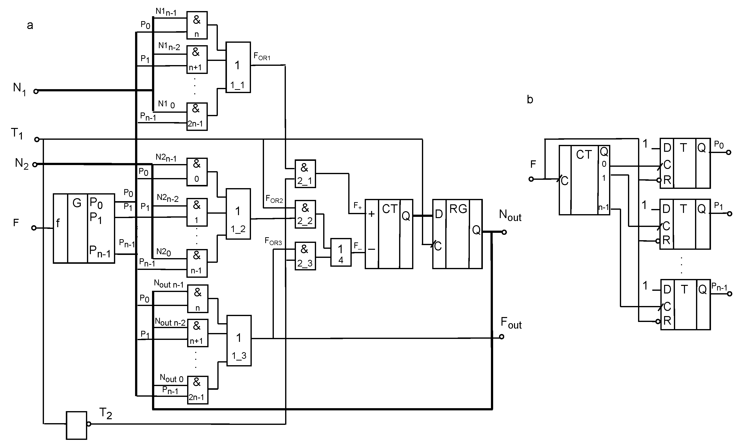
2. Design of the Converter

Transformations of pulse signals from sensors can be performed in different ways. Let us consider the implementation of the converter, for example, for a temperature sensor, which forms a signal in PWM form. This signal is formed by a semiconductor sensing element and is digitized with a first-order sigma–delta modulator. The output signal is a periodic signal represented by time intervals T 1 (high level) and T 2 (low level). The conversion function of the temperature sensor is as follows:
T ( C ) = a 1 + a 2 T 1 T 2 .
where a 1 and a 2 are constants determined by the sensor model.

2.1. Implementation Based on Traditional Calculations

The sensor output signal is quasi-digital and can be processed by digital elements. Sensor manufacturers recommend two approaches to temperature calculation based on the parameters of the output signal [15]. Firstly, it can be a software implementation oriented to the usage of the microcontrollers. Most microcontrollers allow direct connection of sensitive elements, forming a quasi-digital output signal, to the input ports. Using a microcontroller allows you to implement simple, inexpensive solutions, but errors in the result may occur. The source of such errors is software-dependent effects. The analysis and options for compensating such effects are given in [16]. Secondly, the transformations can be performed by hardware using typical computing units. The schematic recommended by the manufacturer of a temperature sensor with output characteristic (1) is given in [15]. The circuit measures the duration of the output single signals from the sensor with a resolution of ±1 µs. For this purpose, a cascade connection of 8-bit counters is used. The counters start with the rising edge of the sensor signal and count clock pulses from an external 1 MHz oscillator. The counting results are stored in the output registers. The falling edge of the signal from the sensor forms the reset signal for the counters. After that, they start counting the next output phase—the duration of the zero value of the sensor output signal. The calculated value at the beginning of the new period is also stored in the registers. Then, the obtained values T 1 and T 2 are used to calculate the temperature by hardware or to transmit it to the software computing core.

2.2. Implementation Based on the Method of Small Increments

Consider the pulse stream implementation of expression (1). A schematic of the n-digit device realizing this operation is shown in Figure 1a. A reference pulse stream is sent to the input F and the generator G forms n reference pulse streams based on the F. Generation of reference pulse streams is performed as follows (Figure 1b). Each pulse of the F stream increases the value of the CT counter by one. At the same time, one of the outputs of this counter switches from the state “0” to “1”. The only exception is the counter change from the state “all ones” to the state “all zeros”, when none of the outputs switch from “0” to “1”. The output signals of the counter are used as clock signals for the triggers T. In these triggers, a one is written when a rising edge occurs at the counter output. Obviously, for every F-flow pulse a one is written to no more than one trigger. After the falling edge of the F-flow pulse all triggers are reset. Thus, the sum of pulses in all generated streams is equal to 2 n 1 during the device operation period.
The average frequencies of P i streams over the period of device operation are determined as follows:
P i = F 2 n 2 n i 1
where i∈ [0 : n – 1].
Logic elements & 0 & n 1 , connected to the outputs of generator G, implement the function of multiplication of streams P i by bits of binary code N. The resulting streams are summed by the OR logic element. The logic expression for the output of this element is as follows:
F O R 1 = L 0 L 1 L 2 L n 1 .
The function L in the general case for each i-th input of element OR1 is formed on the corresponding elements of & i :
L i = N 1 n i 1 P i 2 n ,
where N 1 n i 1 is the logical state of the n-i-1 digit of the code N 1 ; P i is the pulse stream from the generator G output.
The pulse streams at the outputs of elements & 0 & n 1 have the following frequencies:
L 0 = N 1 n 1 P 0 , L 1 = N 1 n 2 P 1 , L 2 = N 1 n 3 P 2 , , L n 1 = N 1 0 P n 1 .
The total value of the frequency F O R 1 at the output of the OR1 element is determined as follows:
F O R 1 = N 1 n 1 P 0 + N 1 n 2 P 1 + N 1 n 3 P 2 + + N 1 0 P n 1 = F 2 n N 1 n 1 2 n 1 + N 1 n 2 2 n 2 + N 1 n 3 2 n 3 + + N 1 0 2 0 .
In this expression, the sum of the products of the current code bit N 1 i by the weight of the n-bit code bit is the binary code N 1 . Thus, the average frequency of the pulse stream at the output of the OR1 logic element can be written as follows:
F O R 1 = F 2 n N 1
Similarly, the value of frequencies F O R 2 and F O R 3 at the outputs of elements OR2 and OR3, respectively, is determined as:
F O R 2 = F 2 n N 2 and F O R 3 = F 2 n N o u t
Consider the operation of the converter shown in Figure 1a. Let the initial moment of time zero code be stored in the counter and register, i.e., N o u t = 0 . At digital inputs N 1 and N 2 , the binary codes corresponding to constants a 1 and a 2 of Equation (1) are set. The reference pulse stream is supplied to input F; the PWM signal from the sensor output is received at input T 1 . Elements 1 1 and 1 2 , under the influence of codes N 1 and N 2 , form the streams F O R 1 and F O R 2 . During the first period, as long as the input T 1 holds signal value “1”, the stream F O R 2 passes through the element & 2 2 and 1 4 to the counter input marked as “−”. When the value at input T 1 becomes zero, the stream F O R 2 is blocked. At this time, the stream F O R 1 starts flowing through element & 2 1 to the counter input marked “+”. The stream F O R 3 is not generated because of the zero code N o u t . When the signal “1” appears on the input of T 1 again, the counted number of pulses from the counter CT is rewritten into the register RG. While T 1 = 1 at the counter input “−” the stream F O R 2 passes, when T 1 = 0 at the counter input “+” the stream F O R 1 passes, and at the counter input “−” the F O R 3 stream is formed on the basis of the zero code N o u t = 0 . Negative feedback is used in the device, and as a result, the dynamic equilibrium mode is reached. In this mode, the number of pulses coming to the adding N + and subtracting N inputs of the counter CT during the period T is the same, i.e.,
N = N + or F ¯ = F ¯ +
where F ¯ + and F ¯ are the average values of pulse flux frequencies at the counter inputs “−” and “+”, respectively.
The “+” counter input receives pulses during the device’s operating period T. The number of pulses is determined by the following expression:
F + = F O R 1 T 2 = F 2 n N 1 T 2 .
The number of pulses that come to the input of the counter “−” during the period of operation of the device T is calculated as follows:
F = T 1 F O R 2 + T 2 F O R 3 = F 2 n T 1 N 2 + T 2 N o u t
In the dynamic equilibrium mode, the characteristic (2) with regard to (3) and (4) will have the following form:
F 2 n N 1 T 2 = F 2 n T 1 N 2 + T 2 N o u t
From the last expression, we get the equation:
N o u t = N 1 N 2 T 1 T 2
That is, the characteristic of the device corresponds to the function of the sensor.

3. Converter Implementation

To study the functioning of the proposed circuit, we developed a description of the device in VerilogHDL.

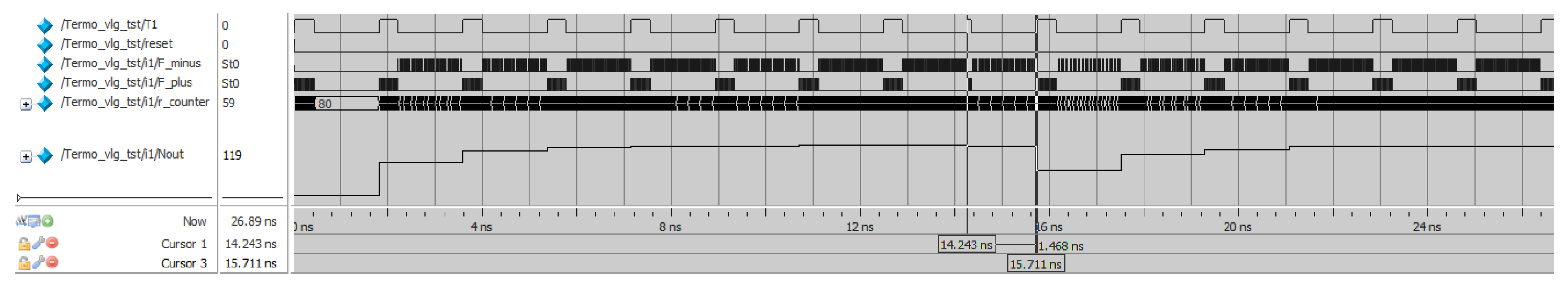
3.1. Simulation of the Converter

The input signals for the program are the reference frequency signal F and the input signal T consisting of two parts: T 1 and T 2 . For the correct operation of the model, an additional reset signal is used to ensure that the counters and registers are set to a zero state. However, given that the device has a steady state and always tends to it, it can start from any random state, so the reset signal is optional. The input signals for the program are the reference frequency signal F and the input signal T, consisting of two parts: T 1 and T 2 . For the correct operation of the model, an additional reset signal is used to ensure that the counters and registers are set to a zero state. However, given that the device has a steady state and always tends to it, it can start from any random state, so the reset signal is optional. The constants in the implemented expression are set at the stage of synthesis; in the program, they are described as parameters. When creating a universal device, additional digital inputs can be provided for these constants. Figure 2 shows the operation of the device configured to process the signal from the AD TMP03 temperature sensor.
The diagram shows the transient process, during which the transducer reaches the equilibrium mode. Starting from the fifth period of the input signal T 1 , the transducer keeps the output code unchanged. This code is the result of the execution of transformations. At the moment of 14.243 ns, an interference occurs, which leads to a shortening of the signal duration T 1 . After three periods, the converter returns to the equilibrium mode, compensating for the failure by triggering the feedback.

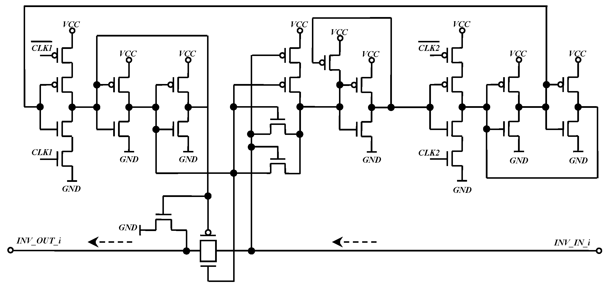
3.2. Custom Circuit Design

Despite the fact that the layout design of elements such as registers, counters, or logic primitives is quite well developed, research on topology optimization continues. This research is related to the search for original solutions in order to optimize the chip area, power and speed [17,18]. When minimizing the circuit layout design, we are looking for solutions that minimize the main component of pulse stream information processing devices—the binary counter. Solutions based on the principle of “first-zero search” are proposed. The circuit diagram of the counter cell based on the “first zero search” principle is shown in Figure 3. Its current–discharge inversion control circuit is built on pass-through keys (as in Manchester adder transfer circuits). The cells are combined into four-digit sections with an inverter at the input and at the output. At the input of each i-th bit from the previous one comes the I N V _ I N _ i signal to invert the value of the current bit. If the inversion control signal is changed, the pass-through key in the circuit is opened. This cuts off the low-order bits and generates a new I N V _ O U T _ i control signal value (cancelling the inversion of the current bit) in the cell. This value is sent to the next (high) counter digit.
The considered circuit solution provides not only high speed and low hardware costs, but also a linear dependence of the delay time and on-chip area on the bit resolution of the device. Moreover, if necessary, the proposed circuit solution can significantly increase the speed of circuits with a relatively small increase in the area on the chip. Figure 4 shows an example of topological implementation of the converter considered above (Figure 1) for 4-bit data. Matrixing of the presented topology along the ordinate axis with an appropriate matrixing coefficient makes it possible to obtain a device of the required digit capacity (a multiple of four). The topology was developed using the original computer-aided design tools [19] in a technologically invariant concept, which allows the design to be adjusted to the design and technological requirements of the chosen manufacturing enterprise.
From the presented material, we can see that the implementation of such calculators in the form of independent fragments of integrated circuits is compact and simple. In addition, it has greater speed than devices based on universal computing units.

4. Conclusions

A large number of sensors provide information in pulse form. This is due to the simplicity of obtaining a pulse signal at the output of the sensing element, as well as the following advantages of the pulse form:
  • Energy efficiency of the presence of pauses between pulses, which reduces the average power consumption;
  • High reliability of information transmission by a stream of pulses, since the loss of one pulse when transmitting a number of pulses is equivalent to the loss of one low-order bit of the binary code, while the loss of a pulse when transmitting a binary code, even in sequential format, is equivalent to the loss of a value with the weight 2 k , where k is a bit number in the binary code.
In this paper, we proposed a new method of functional processing of pulse streams based on elementary logical and arithmetic operations (increment/decrement) and implemented using simple digital elements: logic primitives, counters and registers without using an adder, multiplier, divider or other complex nodes. The considered device provides division of PWM signals directly in pulse form without additional conversion into digital binary codes. This device can be implemented based on PLD and used as an interface for sensors that generate PWM output signal and require multiplying and dividing operations. Small corrections will allow the proposed structure to be used to process signals of a large number of existing quasi-digital sensors with frequency and pulse-width modulated outputs, which are available at the moment.

Author Contributions

Conceptualization, O.B. and N.S.; methodology, O.B.; software, S.M.; validation, S.M., Z.S. and N.S.; formal analysis, O.B.; investigation, S.M. and Z.S.; resources, N.S.; writing—original draft preparation, O.B.; writing—review and editing, Z.S.; visualization, S.M.; supervision, N.S.; project administration, O.B.; funding acquisition, O.B. All authors have read and agreed to the published version of the manuscript.

Funding

This work was supported by the Ministry of Science and Higher Education of the Russian Federation by the Agreement No. 075-15-2022-291 dated 15 April 2022 on the provision of a grant in the form of subsidies from the federal budget for the implementation of state support for the establishment and development of the world-class scientific center «Pavlov center Integrative physiology for medicine, high-tech healthcare, and stress-resilience technologies».

Institutional Review Board Statement

Not applicable.

Informed Consent Statement

Not applicable.

Data Availability Statement

Not applicable.

Conflicts of Interest

The authors declare no conflict of interest.

References

  1. Jain, R.; Tata, S. Cloud to Edge: Distributed Deployment of Process-Aware IoT Applications. In Proceedings of the 2017 IEEE International Conference on Edge Computing (EDGE), Honolulu, HI, USA, 25–30 June 2017; pp. 182–189. [Google Scholar]
  2. Singh, S. Optimize cloud computations using edge computing. In Proceedings of the 017 International Conference on Big Data, IoT and Data Science (BID), Pune, India, 20–22 December 2017; pp. 49–53. [Google Scholar]
  3. Feichi, Z.; Yang, C. Near-sensor and in-sensor computing. Nat. Electron. 2020, 3, 664–671. [Google Scholar]
  4. Yang, C. In-sensor computing for machine vision. Nature 2020, 579, 32–33. [Google Scholar]
  5. Ueno, K.; Asai, T.; Amemiya, Y. Temperature-to-frequency converter consisting of subthreshold mosfet circuits for smart temperature-sensor LSIs. In Proceedings of the TRANSDUCERS 2009-2009 International Solid-State Sensors, Actuators and Microsystems Conference, Denver, CO, USA, 21–25 June 2009; pp. 2433–2436. [Google Scholar]
  6. Beshliu, V.S.; Kantser, V.G.; Beldiman, L.N.; Beshliu, V.V.; Coban, R.A. Integral gauge pressure sensor with frequency output signal. In Proceedings of the CAS ’99 Proceedings. 1999 International Semiconductor Conference (Cat. No.99TH8389), Sinaia, Romania, 5–9 October 1999; pp. 491–494. [Google Scholar]
  7. Darwish, H.; Reig, C.; Cubells-Beltrán, M.D.; Leger, G.; De Marcellis, A. CMOS Capacitance-to-Time Converter-Based Interface for Differential Capacitive Sensors. In Proceedings of the 2020 Global Congress on Electrical Engineering (GC-ElecEng), Valencia, Spain, 4–6 September 2020; pp. 61–64. [Google Scholar]
  8. Kokolanski, Z.; Gavrovski, C.; Dimcev, V.; Makraduli, M. Simple Interface for Resistive Sensors Based on Pulse Width Modulation. Trans. Instrum. Meas. 2013, 62, 2983–2992. [Google Scholar] [CrossRef]
  9. Arbet, D.; Kováč, M.; Stopjaková, V.; Potočný, M. Voltage-to-Frequency Converter for Ultra-Low-Voltage Applications. In Proceedings of the 2019 42nd International Convention on Information and Communication Technology, Electronics and Microelectronics (MIPRO), Opatija, Croatia, 20–24 May 2019; pp. 53–58. [Google Scholar]
  10. Areekath, L.; George, B.; Reverter, F. An Auto-Balancing Capacitance-to-Pulse-Width Converter for Capacitive Sensors. IEEE Sens. J. 2021, 21, 765–775. [Google Scholar] [CrossRef]
  11. Safyannikov, N.; Bureneva, O. Bit-Stream Functional Converters for Decentralized Sensor Systems. In Proceedings of the 2020 9th Mediterranean Conference on Embedded Computing (MECO), Budva, Montenegro, 8–11 June 2020; pp. 1–4. [Google Scholar]
  12. Santos, E.J.P.; Silva, L.B.M. FPGA-based smart sensor implementation with precise frequency to digital converter for flow measurement. In Proceedings of the 2010 VI Southern Programmable Logic Conference (SPL), Ipojuca, Brazil, 24–26 March 2010; pp. 21–26. [Google Scholar]
  13. Tirupathi, R.; Kar, S.K. On-Chip Implementable Autocalibration of Sensor Offset for Differential Capacitive Sensor Interfaces. IEEE Trans. Instrum. Meas. 2021, 70, 1–9. [Google Scholar] [CrossRef]
  14. Yoshii, Y.; Nakajo, A.; Abe, H.; Nimomiya, K.; Miyashita, H.; Sakurai, N.; Kosuge, M.; Hao, S. 1 chip integrated software calibrated CMOS pressure sensor with MCU, A/D convertor, D/A convertor, digital communication port, signal conditioning circuit and temperature sensor. In Proceedings of the International Solid State Sensors and Actuators Conference (Transducers ’97), Chicago, IL, USA, 19 June 1997; pp. 1485–1488. [Google Scholar]
  15. Serial Digital Output Thermometers. Analog Device. Available online: https://www.analog.com/media/en/technical-documentation/data-sheets/ (accessed on 10 October 2021).
  16. Reverter, F.; Jordana, J.; Pallas-Areny, R. Program-dependent uncertainty in period-to-code converters based on counters embedded in microcontrollers. In Proceedings of the 20th IEEE Instrumentation Technology Conference (Cat. No.03CH37412), Vail, CO, USA, 20–22 May 2003; pp. 977–980. [Google Scholar]
  17. Thakur, A.; Mehra, R. Power and speed efficient ripple counter design using 45 nm technology. In Proceedings of the 2016 IEEE 1st International Conference on Power Electronics, Intelligent Control and Energy Systems (ICPEICES), Delhi, India, 4–6 July 2016; pp. 1–4. [Google Scholar]
  18. Putra, H.D.; Pratiwi, S.E.; Jamilah, W. The synthesis of counter circuit layout design based on CMOS technology 0.35 micro-m. In Proceedings of the 2017 Second International Conference on Informatics and Computing (ICIC), Jayapura, Indonesia, 1–3 November 2017; pp. 1–5. [Google Scholar]
  19. Mironov, S.E.; Zibarev, K.M. Management of Layout Matching of Objects of Complex Microelectronic Systems with Uncertainty of Design Rules. In Proceedings of the 2019 III International Conference on Control in Technical Systems (CTS), St. Petersburg, Russia, 30 October–1 November 2019; pp. 69–73. [Google Scholar]
Figure 1. (a) General circuit diagram of the converter; (b) circuit diagram of the reference pulse signal generator G.
Engproc 33 00050 g001
Figure 2. Result of the converter simulation.
Engproc 33 00050 g002
Figure 3. Electrical diagram of the single-digit counter cell “+1”.
Engproc 33 00050 g003
Figure 4. Layout design of the 4-digit calculator section.
Engproc 33 00050 g004
Disclaimer/Publisher’s Note: The statements, opinions and data contained in all publications are solely those of the individual author(s) and contributor(s) and not of MDPI and/or the editor(s). MDPI and/or the editor(s) disclaim responsibility for any injury to people or property resulting from any ideas, methods, instructions or products referred to in the content.

