Proceeding Paper

Rapid, Low-Cost Production of Multilayer Molds for PDMS Lab-on-Chip Devices †

by
Eldas M. Maesela
1,2,
Mandla Msimanga
2,
Masibulele Kakaza
1 and
Manfred R. Scriba
1,*
1
Future Production: Chemicals, Centre for Nano-Structured and Advanced Materials, Council for Scientific and Industrial Research, Pretoria 0184, South Africa
2
Department of Physics, Faculty of Science, Tshwane University of Technology, Pretoria 0083, South Africa
*
Author to whom correspondence should be addressed.
Presented at the Micro Manufacturing Convergence Conference, Stellenbosch, South Africa, 7–9 July 2024.
Eng. Proc. 2025, 109(1), 3; https://doi.org/10.3390/engproc2025109003
Published: 8 September 2025

Abstract

We present a simple, rapid and low-cost multi-layer mold fabrication method for production of polydimethylsiloxane (PDMS) lab-on-chip (LOC) devices. The new approach offers resource-strained researchers access to microfluidic lab-on-chip fabrication for medical diagnostics, food security and environmental monitoring applications. In this work, photomasks were designed on PowerPoint (2021) and printed on Pelikan transparency sheets using a Canon PIXMA iX6840 Inkjet printer. The photomasks were then tested for ultraviolet (UV) transmission and compared to the masks produced for circuit board manufacture. Another low-cost approach for the alignment of multi-exposure masks was also developed and tested by producing three-layer photoresist pyramid-like structures on silicon (Si) wafer using the soft lithography process.

1. Introduction

Lab-on-chip (LOC) devices are small platforms that incorporate multiple laboratory functions on a single device that is generally not larger than credit card [1] and have already impacted the fields of analytical chemistry and biomedical sciences [1,2,3]. In LOC devices, disciplines such as microfluids, biochemistry, materials and engineering converge to deliver innovative opportunities in diagnostics, drug discovery, environmental monitoring and personalized medicine [4].
For LOC device development, polydimethylsiloxane (PDMS) is the preferred material for the manufacture due to its biocompatibility, optical transparency and easy manufacturing using soft lithography technology [4,5,6]. The development of a PDMS device involves the creation of molds using photolithography or 3D printing and then casting PDMS to transfer the microstructures from the mold to the LOC [6,7,8,9]. To produce multilayer PDMS details, the mold must accommodate additional layers of SU-8 photoresist which can be patterned and etched sequentially to produce the 3D structure [10,11]. The ability to form multiple layers in a microfluidic lab-on-chip (LOC) mold offers developers the benefit of incorporating increased and complex functionality in the device [10,12]. The alignment between these layers is essential to ensure the proper registration of features and avoid errors that could compromise the functionality of the device [11]. Typically, the dimensions of the LOC features lie between 10 and 100 um and their alignment accuracy depends on the device functionality and complexity [13]. For our applications, the alignment error of 25 um is acceptable as we design structures with dimensions of at least 100 um. This paper describes an innovative approach for the rapid and low-cost production of multilayer master molds for the manufacture of PDMS Lab-on-Chip devices.

2. Materials and Methods

2.1. Mask Production

Masks for 3-layered square and round pyramids were designed in Microsoft PowerPoint (2021), including the corresponding alignment marks on each of the 3 masks. The masks were printed on Pelikan overhead transparency film OH501 724211 (Manufactured in Hannover, Germany) of 135 um thickness and specified to accommodate a 9600 dpi printing, using a Canon PIXMA iX6840 Inkjet printer (Manufactured by Canon: Tokyo, Japan) with a matching resolution. The bottom, middle and top masks are shown in Figure 1. As the black areas in the mask must block UV light transmission during photoresist exposure, the printer was set to the maximum print density in picture printing mode. The dimensional accuracy of the features of the masks was determined by microscope to be in the range of the dot size approximately ±5 um.
To make sure that the transparency and blocking ability of an inkjet printer mask compares well to scanning laser produced printed circuit board (PCB) mask. The proper alignment of these features was accomplished by incorporating cross and line (+ and −) marks at the bottom of each mask as indicated in Figure 1.

2.2. Mask Alignment and Silicon Wafer Holder for UV Exposure

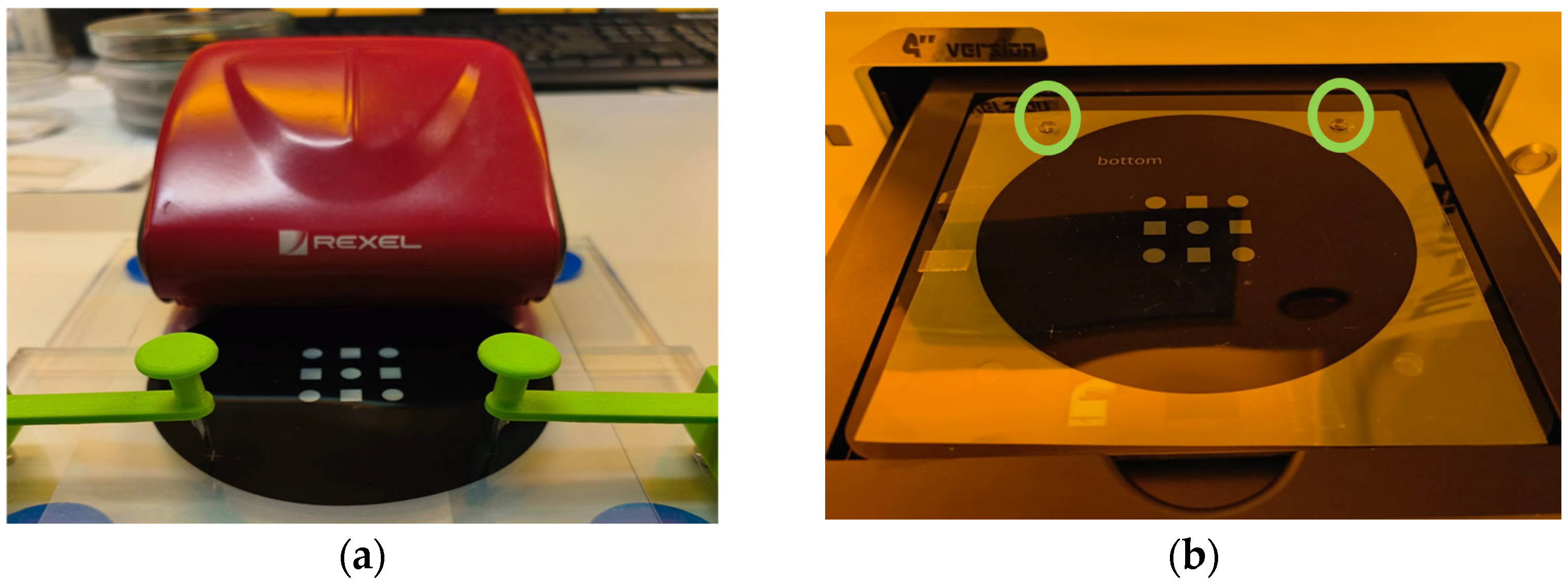
Two alignment holes were punched into the mask with a simple paper punch mounded on a laser cut base (Figure 2a) and held in place by two needle pins positioned on alignment marks. Prior to UV exposure, these punched holes were positioned on two protruding pins on the mask ho holder (Figure 2b) to achieve good alignment of all masks.

2.3. SU-8 Mold Fabrication

The silicon wafer of 100 mm diameter was first cleaned with isopropanol, then rinsed with acetone and subsequently kept at 120 °C for 15 min to remove all moisture on the surface. The SU-8 2075 photoresist was then applied on the wafer by spin coating. Afterwards, the wafer was kept at 65 °C for 1 min and 95 °C for 5 min and cooled down to room temperature, followed by UV exposure using a UV-KUB 2 produced by KLOÉ, France. Exposure times of 5, 10 and 15 s were adequate to achieve a cross linkage of the first, second and third photoresist layers, whereafter the wafer was kept at 65 °C for 1 min and 95 °C for 5 min and cooled down to room temperature. The baking process for the second layer was 65 °C for 5 min and 95 °C for 15 min and the third layer was 65 °C for 8 min and 95 °C for 25 min. SU-8 developer was then applied for 30 min on the wafer to remove un-cured photoresist, rinsed with isopropanol and dried with liquid nitrogen and revealed the hardened negative 3-layer mold, as shown in Figure 3.

3. Results and Discussions

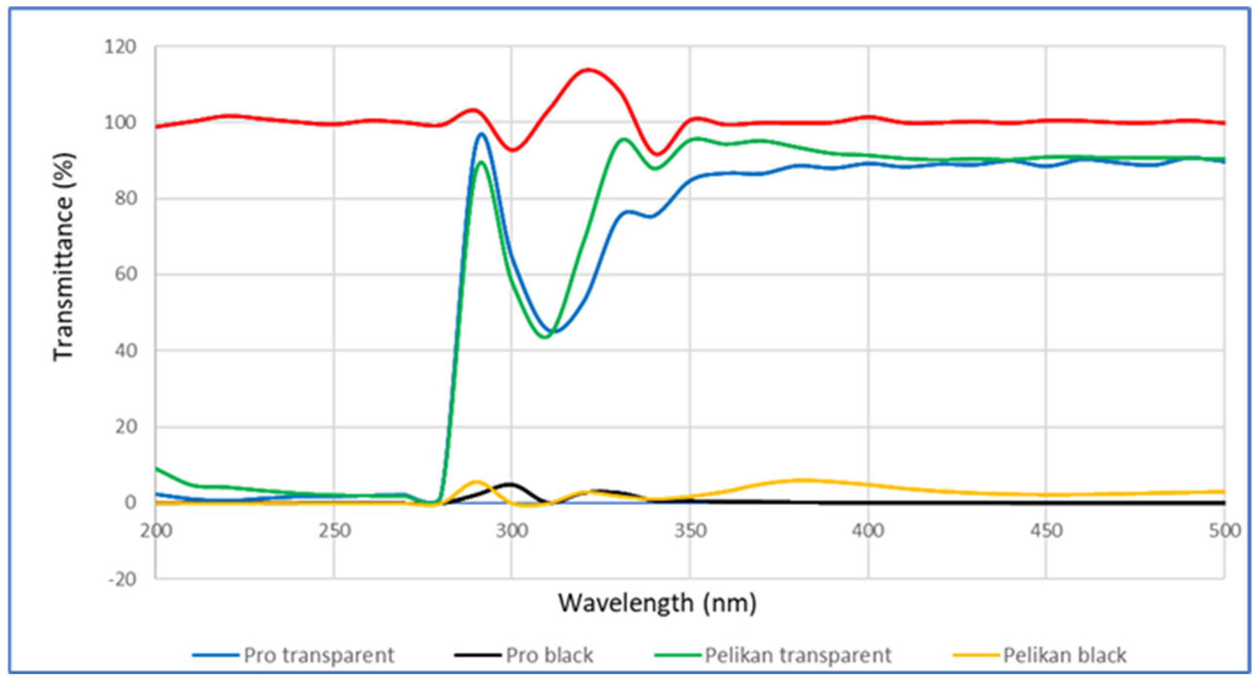
Photomasks were successfully printed on a Canon PIXMA iX6840 Inkjet printer on transparency film, and alignment accuracy was estimated by measuring the symmetry in the placement of layers in the pyramid structure using Image J. An estimated alignment accuracy of about ±20 µm can be achieved with our low-cost approach, thus offering resource strained researchers a chance to produce LOC devices. Alignment in both directions was very similar and hence only the X-direction is presented. Calibration was achieved by using an accurately measured disk. Photomasks printed on Pelikan transparency sheets as well as laser scribed photomasks supplied by a PCB manufacturer, were tested for UV transmission, as shown in Figure 4. The films are transparent in the UV region below 300 nm, and both inkjet-printed and PCB masks adequately block UV transmission as required.

Author Contributions

Conceptualization, M.R.S.; methodology, M.R.S., M.K. and E.M.M.; validation, E.M.M. and M.M.; investigation, E.M.M.; writing—original draft preparation, E.M.M.; writing—review and editing, M.R.S. and E.M.M. All authors have read and agreed to the published version of the manuscript.

Funding

This research was part of a Department of Science and Innovation (DSI)-funded project with the Council of Scientific and Industria Research project number C6BCH45.

Institutional Review Board Statement

Not applicable.

Informed Consent Statement

Not applicable.

Data Availability Statement

The raw data supporting the conclusions of this article will be made available by the authors on request.

Acknowledgments

Authors would like to acknowledge the support of the Council for Scientific and Industrial Research and the DSI as well as the organizers of the Micro Manufacturing Conference 2024 for their support and the opportunity to present this work.

Conflicts of Interest

Manfred Scriba, Eldas M. Maesela and Masibulele Kakaza are employed by the company CSIR, Centre for Nano-Structured and Advanced Materials and declare that the research was conducted in the absence of any commercial or financial relationships that could be construed as a potential conflict of interest.

References

  1. Zhuang, J.; Yin, J.; Lv, S.; Wang, B.; Mu, Y. Advanced “lab-on-a-chip” to detect viruses—Current challenges and future perspectives. Biosens. Bioelectron. 2020, 163, 112291. [Google Scholar] [CrossRef] [PubMed]
  2. Zhu, H.; Fohlerová, Z.; Pekárek, J.; Basova, E.; Neužil, P. Recent advances in lab-on-a-chip technologies for viral diagnosis. Biosens. Bioelectron. 2020, 153, 112041. [Google Scholar] [CrossRef] [PubMed]
  3. Dkhar, D.S.; Kumari, R.; Malode, S.J.; Shetti, N.P.; Chandra, P. Integrated lab-on-a-chip devices: Fabrication methodologies, transduction system for sensing purposes. J. Pharm. Biomed. Anal. 2023, 223, 115120. [Google Scholar] [CrossRef] [PubMed]
  4. Zhang, G.; Sun, Y.; Qian, B.; Gao, H.; Zuo, D. Experimental study on mechanical performance of polydimethylsiloxane (PDMS) at various temperatures. Polym. Test. 2020, 90, 106670. [Google Scholar] [CrossRef]
  5. Liu, J.; Yao, Y.; Li, X.; Zhang, Z. Fabrication of advanced polydimethylsiloxane-based functional materials: Bulk modifications and surface functionalizations. Chem. Eng. J. 2021, 408, 127262. [Google Scholar] [CrossRef]
  6. Ariati, R.; Sales, F.; Souza, A.; Lima, R.A.; Ribeiro, J. Polydimethylsiloxane composites characterization and its applications: A review. Polymers 2021, 13, 4258. [Google Scholar] [CrossRef] [PubMed]
  7. Kang, H.; Lee, D.; Yang, Y.; Oh, D.K.; Seong, J.; Kim, J.; Jeon, N.; Kang, D.; Rho, J. Emerging low-cost, large-scale photonic platforms with soft lithography and self-assembly. Photonics Insights 2023, 2, R04. [Google Scholar] [CrossRef]
  8. Deng, J.; Jiang, L.; Si, B.; Zhou, H.; Dong, J.; Cohen, P. AFM-Based nanofabrication and quality inspection of three-dimensional nanotemplates for soft lithography. J. Manuf. Process. 2021, 66, 565–573. [Google Scholar] [CrossRef]
  9. Xu, Y.; Liu, M.; Kong, N.; Liu, J. Lab-on-paper micro- and nano-analytical devices: Fabrication, modification, detection and emerging applications. Microchim. Acta 2016, 183, 1521–1542. [Google Scholar] [CrossRef]
  10. Gao, S.; Zhan, T.; Zhou, W.; Niu, F.; Min, S.; Xiao, A.; Xu, B. Mold Embossing-Based Soft Lithography for Fabrication of Complex Non-rectangular Channels. ACS Appl. Mater. Interfaces 2023, 15, 31755–31764. [Google Scholar] [CrossRef] [PubMed]
  11. Koucherian, N.E.; Yan, S.; Hui, E.E. Fabrication of Multilayer Molds by Dry Film Photoresist. Micromachines 2022, 13, 1583. [Google Scholar] [CrossRef] [PubMed]
  12. Nguyen, T.; Sarkar, T.; Tran, T.; Moinuddin, S.M.; Saha, D.; Ahsan, F. Multilayer Soft Photolithography Fabrication of Microfluidic Devices Using a Custom-Built Wafer-Scale PDMS Slab Aligner and Cost-Efficient Equipment. Micromachines 2022, 13, 1357. [Google Scholar] [CrossRef] [PubMed]
  13. Scott, S.M.; Ali, Z. Fabrication methods for microfluidic devices: An overview. Micromachines 2021, 12, 319. [Google Scholar] [CrossRef] [PubMed]
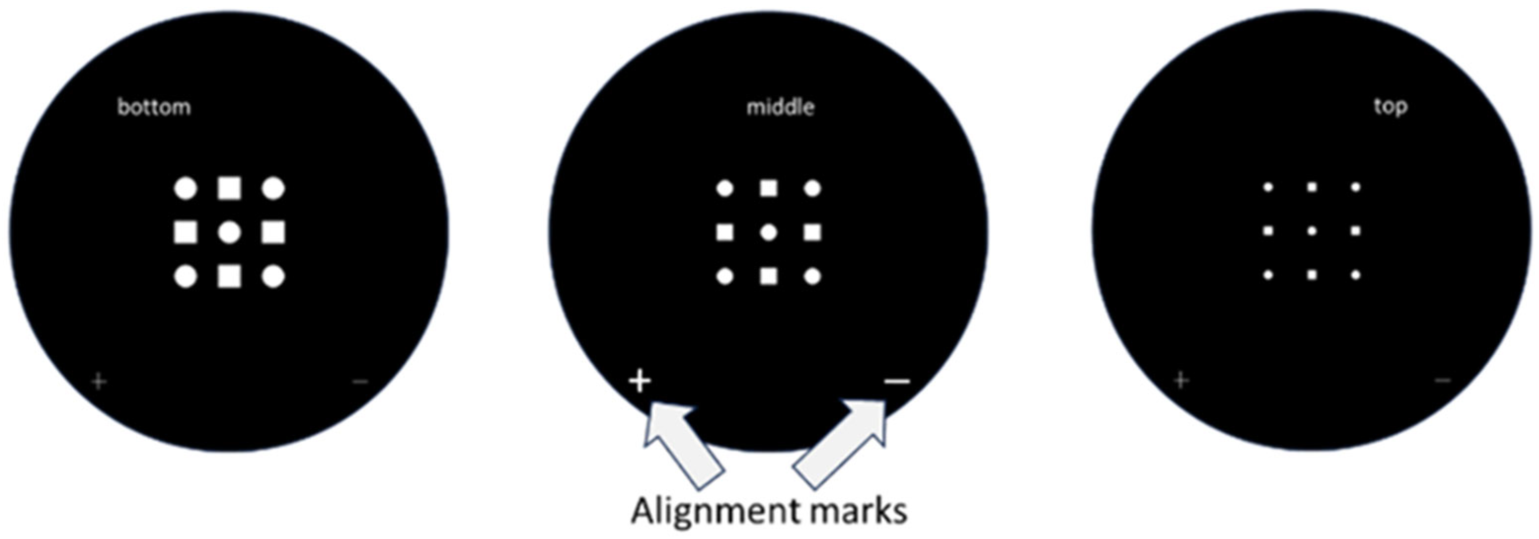
Figure 1. Inkjet-printed masks for a 3-layer mold fabrication.
Engproc 109 00003 g001
Figure 2. (a) Mask alignment punch; (b) Si wafer and mask jig in a UV-KUB 2 tray.
Engproc 109 00003 g002
Figure 3. Disk and square three-layer pyramid master molds were created, and the alignment accuracy was measured using a Meiji Techno microscope (EMZ-8TR).
Engproc 109 00003 g003
Figure 4. UV–vis measurements of the Pelikan transparent sheet photomask compared to the Procircuit photomasks. The red line represents free transmission of the measurement beam.
Engproc 109 00003 g004
Disclaimer/Publisher’s Note: The statements, opinions and data contained in all publications are solely those of the individual author(s) and contributor(s) and not of MDPI and/or the editor(s). MDPI and/or the editor(s) disclaim responsibility for any injury to people or property resulting from any ideas, methods, instructions or products referred to in the content.