Proceeding Paper

Addressing Manufacturing and Cost Challenges Toward Solving Low-Cost In Situ Digital Holographic Microscopy Problems †

by
Larissa Hurter
*,
Heinrich Edgar Arnold Laue
* and
Johan Schoeman
*
Department of Electrical, Electronic and Computer Engineering, University of Pretoria, Hatfield, Pretoria 0002, South Africa
*
Authors to whom correspondence should be addressed.
Presented at the Micro Manufacturing Convergence Conference, Stellenbosch, South Africa, 7–9 July 2024.
Eng. Proc. 2025, 109(1), 14; https://doi.org/10.3390/engproc2025109014
Published: 16 September 2025
(This article belongs to the Proceedings of Micro Manufacturing Convergence Conference)

Abstract

Digital holographic microscopes provide a microscopy solution with a resolution in the low-micrometre range that offers similar performance to optical microscopy, but as a relatively low-cost alternative. The most significant cost saving is due to the ability to reconstruct microscopic images from holograms using low-cost components without the need for an optical stack. The cost saving opens up the avenue towards a feasible solution for geographically distributed in situ microscopic sensing in rural areas for problems like air and water pollution monitoring. The most significant contributors to cost are the camera sensor module, the pinhole, and the processing platform. The latter two components are addressed, at least in part, in this work. We successfully manufactured sub-100 μ m diameter pinholes using ultraviolet (UV) laser cutting with an LPKF printed circuit board (PCB) prototyping platform and present the low-cost micromachining method. The pinholes were utilised within a prototype field-programmable gate array (FPGA) demonstrator that successfully reconstructed the holographic images. The choice for the FPGA approach as the initial step, albeit more complex, lends itself towards the easier development of a dedicated reconstructed application-specific integrated circuit (ASIC) to ultimately drive the cost down even further.

1. Introduction

Digital in-line holographic microscopes (DIHMs) use light from a single point source to illuminate a sample [1]. The sample diffracts some of the light which interferes with the non-diffracted light to form an interference pattern, also known as a hologram, which is captured by a camera sensor [1]. The technique offers a wide field of view (FOV) and allows three-dimensional imaging, making it ideal for observing sparse samples [2,3]. The main factors that limit the resolution achievable by this type of microscope are the temporal coherence of the light source, the distance between the sample and the camera sensor, the camera sensor pixel size, the size of the image used for reconstruction, and the spatial coherence of the light wave emanating from the aperture [4].
The spatial coherence of the light source is improved by decreasing either the ratio of sample-to-camera-sensor distance and light-source-to-sample distance or decreasing the emitting area of the light source [4]. The latter can be accomplished by placing a pinhole between the light source and sample [4]. Pinholes with sub-100 μ m diameters are commonly used [1,5]. Commercially available precision pinholes have limited discrete diameter sizes and are prohibitively expensive, ranging from 49 to 142 USD each [6,7]. Alternative approaches include using a digital micromirror device, an optical fibre and lens assembly, or a cone-shaped optical fibre to create the aperture [8,9,10]. The drawback of pinholes is that the pinhole reduces the amount of light available to form a hologram. This decreases the clarity and signal-to-noise ratio (SNR) of the hologram and faint details get lost in the noise. Quantifying the relationship between aperture size and SNR for a given setup would require a large number of pinholes of varying sizes.
Pinholes with diameters of 50, 100, and 200 μ m have previously been made for a confocal laser scanning microscope on 10 μ m stainless steel foil [11]. The pinholes were made by focusing a laser onto a point of the sheet with an objective lens and then using stepper motors, with step resolutions of 0.1 μ m, to move the platform on which the sheet rests to cut circular holes of the required diameter [11]. A pinhole array with 20 μ m diameter pinholes was made by depositing a 100 nm gold layer on a 200 μ m thick Borofloat33® substrate [12]. The pinhole array pattern was made in the gold layer using the lift-off method [12].
In this paper, we present a technique to quickly and cheaply manufacture pinholes from readily available materials to easily match the manufactured size to the optimal size, which depends on the design and components selected for a particular DIHM application.

2. Materials and Methods

2.1. Sub-100 μ m Pinhole Manufacturing

Pinholes were designed on a printed circuit board (PCB) layout using the LPKF CircuitPro software with diameters of 95, 65, 40, 25, and 20 μ m. Pinholes were manufactured through ultraviolet (UV) laser cutting with an LPKF ProtoLaser U4 PCB prototyping platform. The laser onboard this platform has a focused beam diameter of 20 ± 2 μ m. The pinholes were manufactured on single-sided FR4 PCB sheets with a measured thickness of 0.31 mm. Twenty holes of each size were manufactured, half with the copper layer at the top and the remainder by cutting from the substrate layer at the top.
The material settings were set to 0.36 mm ML104. The pinholes were made by repeating a drilling operation 17 times over a specified location. The drill parameters were set to use concentric fill from the outside as the strategy to create the pinholes. The laser parameters were set to a frequency of 45 kHz and a power of 5.85 W. The laser’s focus point was set to 0.18 mm below the FR4 surface.

2.2. FPGA Reconstruction Algorithm

Methods for reconstructing images, U [ x , y ] , include the angular spectrum method (ASM), Fresnel diffraction method, and methods based on Rayleigh–Sommerfield diffraction theory and the Fresnel diffraction formula [13,14]. The ASM was chosen due to the sample-to-camera-sensor distances used and its comparative computational simplicity. The ASM is given by (adapted from [15])
U [ x , y ] = F 1 F { U 0 [ x 0 , y 0 ] } × e j 2 π z λ 1 ( f x λ ) 2 + ( f y λ ) 2 ,
where U [ x 0 , y 0 ] is the captured image, z is the sample-to-camera-sensor distance, λ is the light source’s peak wavelength, and f x and f y are the spatial frequency matrices. Equation (1) was implemented on an Intel Cyclone V 5CSEMA4U23C6 field-programmable gate array (FPGA) chip.

3. Results

The 20 pinholes of each size were imaged and analysed using an Olympus DX1000 microscope. The diameters of the smallest possible outer circle that encloses the entire hole and the largest possible inner circle that does not cross the edges of the hole itself, as seen in Figure 1, were measured. It was found that the 20 μ m diameter pinholes did not penetrate through the entire sheet. The results of the other four sizes are summarised in Table 1. Circularity, the rightmost column in Table 1, is given as the ratio between the inner and outer circles.
Following our initial observations, additional pinholes with diameters ranging from 20 to 25 μ m were manufactured in 1 μ m increments. The pinholes successfully penetrated the substrate 0, 0, 1, 5, 6, and 10 out of 10 times, respectively.
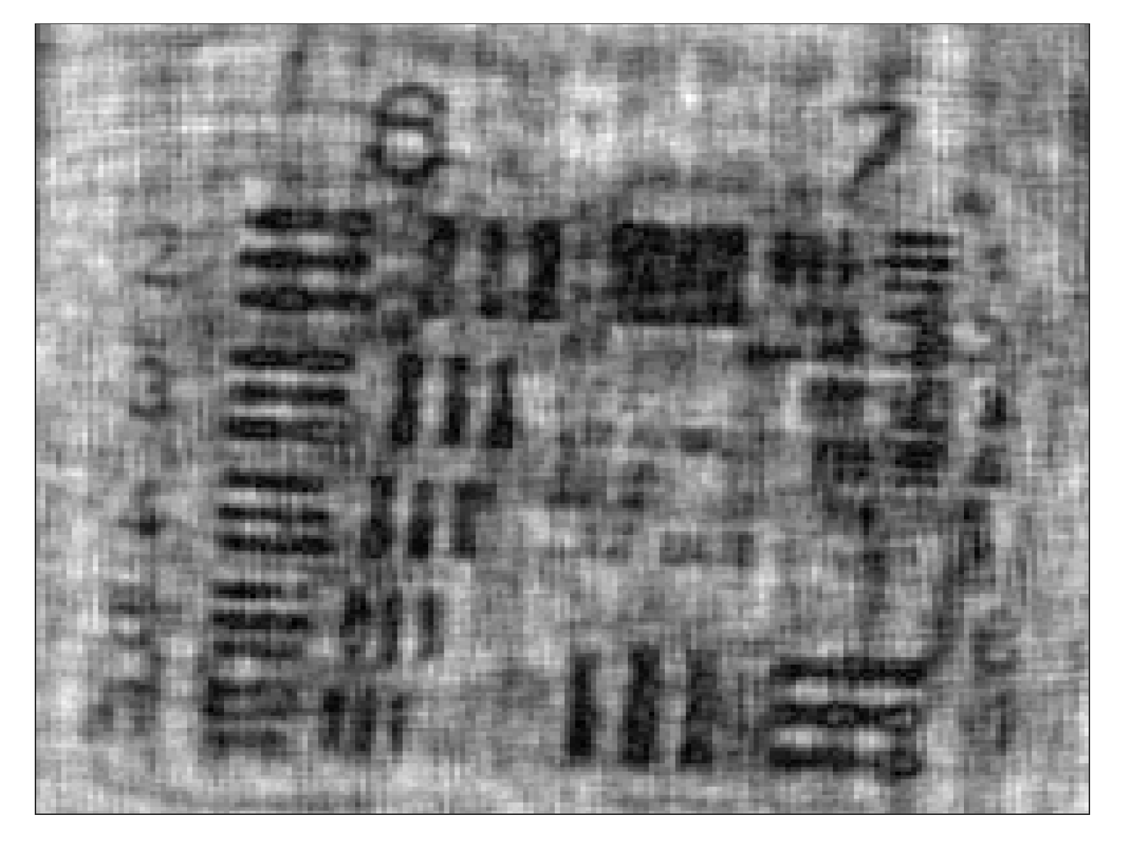
An image of a United States Air Force (USAF) 1951 resolution target was captured when a red light emitting diode (LED) with a spectral bandwidth of 20 nm and a peak wavelength of 640 nm was used with a pinhole with an outer diameter of 27.461 μ m. The resulting 512 × 512 pixel reconstructed image is shown in Figure 2. The group 6 elements of the resolution target have line widths extending from 4.38 to 7.81 μ m and can be distinguished in Figure 2.
The smallest apertures were achieved when cutting from the copper side. Regression was performed on the copper-layer-to-substrate pinhole measurements, leading to the design equation
y = 0.002794 x 2 + 1.232418 x + 4.544506 ,
where y is the pinhole diameter to be specified on the PCB layout and x is the desired outer diameter. Ten pinholes each with desired diameters of 30, 50, and 80 μ m were manufactured to verify Equation (2) as shown in Table 1, with mean outer circle diameters within 2.2, 2.4, and 6.4 μ m of their desired values, respectively.

4. Discussion

Sub-100 μ m pinholes were successfully manufactured using laser cutting on FR4 PCB sheets and used as an aperture for a DIHM to reconstruct images. Objects with micrometre sizes could be distinguished. Pinholes with diameters smaller than 18 μ m were made, below the manufacturer’s specification for the laser (focus beam diameter of 20 ± 2 μ m). Pinholes can be manufactured with a much finer range of values compared to commercially available pinholes using Equation (2). This design equation becomes more inaccurate as the desired pinhole size approaches 95 μ m. The reconstruction was successfully implemented on an FPGA as a precursor to a dedicated application-specific integrated circuit (ASIC).

Author Contributions

Conceptualisation, J.S.; methodology, validation, formal analysis, investigation, and writing, L.H., H.E.A.L. and J.S.; software, L.H.; resources, funding acquisition, and supervision, H.E.A.L. and J.S.; data curation, L.H.; visualisation, L.H. All authors have read and agreed to the published version of the manuscript.

Funding

This work is based on research supported partially by the National Research Foundation of South Africa (Grant Number: 129691) and the South African Department of Science and Innovation Nano and Micro Manufacturing Facility grant.

Institutional Review Board Statement

Not applicable.

Informed Consent Statement

Not applicable.

Data Availability Statement

Dataset available on request from the authors.

Conflicts of Interest

The authors declare no conflicts of interest. The funders had no role in the research or in the decision to publish the results.

Abbreviations

The following abbreviations are used in this manuscript:
ASICApplication-specific integrated circuit
ASMAngular spectrum method
DIHMDigital in-line holographic microscope
FPGAField-programmable gate array
FOVField of view
LEDLight emitting diode
PCBPrinted circuit board
SNRSignal-to-noise ratio
USAFUnited States Air Force
UVUltraviolet

References

  1. Ryle, J.P.; Sheridan, J.T.; McDonnell, S. Lensless multispectral digital in-line holographic microscope. J. Biomed. Opt. 2011, 16, 126004:1–126004:17. [Google Scholar] [CrossRef] [PubMed]
  2. McLeod, E.; Ozcan, A. Unconventional methods of imaging: Computational microscopy and compact implementations. Rep. Prog. Phys. 2016, 79, 076001:1–076001:30. [Google Scholar] [CrossRef] [PubMed]
  3. Wu, Y.; Ozcan, A. Lensless digital holographic microscopy and its applications in biomedicine and environmental monitoring. Methods 2018, 136, 4–16. [Google Scholar] [CrossRef] [PubMed]
  4. Zhang, J.; Sun, J.; Chen, Q.; Zuo, C. Resolution analysis in a lens-free on-chip digital holographic microscope. IEEE Trans. Comput. Imaging 2020, 6, 697–710. [Google Scholar] [CrossRef]
  5. Rostykus, M.; Soulez, F.; Unser, M.; Moser, C. Compact in-line lensfree digital holographic microscope. Methods 2018, 136, 17–23. [Google Scholar] [CrossRef] [PubMed]
  6. Precision Pinholes. Available online: https://www.edmundoptics.com/f/precision-pinholes/12073/ (accessed on 26 July 2024).
  7. Precision Pinholes. Available online: https://ealingcatalog.com/opto-mechanics/apertures/pinholes/precision-pinholes.html (accessed on 26 July 2024).
  8. Maritz, M.G.; Schoeman, J. Programmable aperture using a digital micromirror device for in-line holographic microscopy. IEEE J. Quantum Electron. 2022, 58, 1–8. [Google Scholar] [CrossRef]
  9. Frentz, Z.; Kuehn, S.; Hekstra, D.; Leibler, S. Microbial population dynamics by digital in-line holographic microscopy. Rev. Sci. Instrum. 2010, 81, 084301:1–084301:6. [Google Scholar] [CrossRef] [PubMed]
  10. Patiño-Jurado, B.; Botero-Cadavid, J.F.; Garcia-Sucerquia, J. Optical fiber point-source for digital lensless holographic microscopy. J. Light. Technol. 2019, 37, 5660–5666. [Google Scholar] [CrossRef]
  11. Boutilier, R.M.; Ahn, Y.J.; Park, J.S.; Lee, H. Development of an auto-interchangeable multi-pinhole array for confocal laser scanning microscopy systems using precision laser processing. Opt. Laser Technol. 2019, 116, 58–67. [Google Scholar] [CrossRef]
  12. Endrödy, C.; Mehner, H.; Grewe, A.; Hoffmann, M. Linear micromechanical stepping drive for pinhole array positioning. J. Micromech. Microeng. 2015, 25, 055009:1–055009:9. [Google Scholar] [CrossRef]
  13. Akhter, N.; Min, G.; Kim, J.W.; Lee, B.H. A comparative study of reconstruction algorithms in digital holography. Optik 2013, 124, 2955–2958. [Google Scholar] [CrossRef]
  14. Huaying, W.; Baoqun, Z.; Wei, L. Comparison of the reconstruction algorithms in digital micro-holography. In Proceedings of the IEEE International Conference on Intelligent Computing and Intelligent Systems, Shanghai, China, 20–22 November 2009; Volume 2, pp. 838–842. [Google Scholar]
  15. Goodman, J. Introduction to Fourier Optics; McGraw-Hill: New York, NY, USA, 1996; pp. 55–58. [Google Scholar]
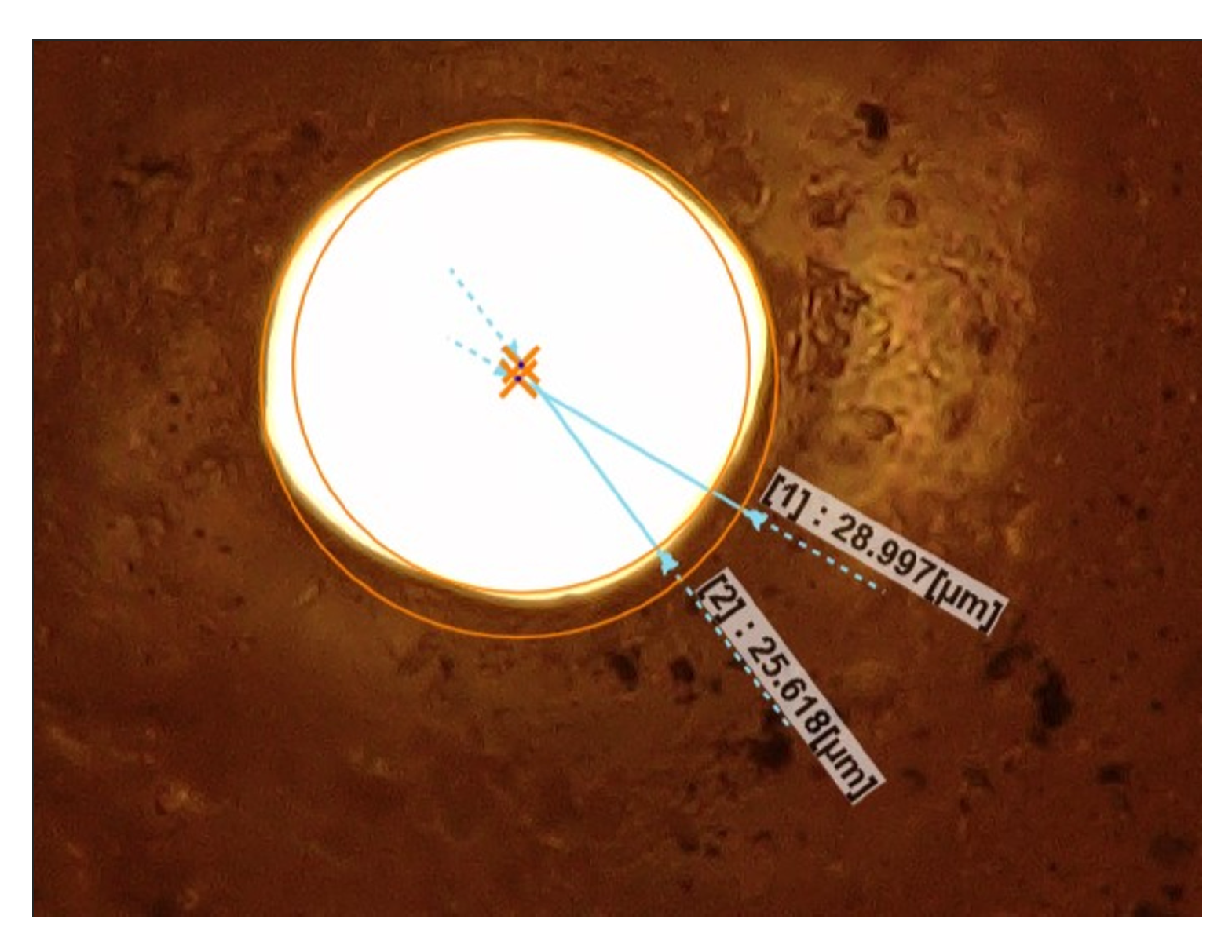
Figure 1. A 65 μ m pinhole with minimum and maximum circles indicated.
Engproc 109 00014 g001
Figure 2. A microscope image of a United States Air Force (USAF) resolution test target reconstructed using a 25 μ m pinhole.
Engproc 109 00014 g002
Table 1. Measurements of pinholes of sizes 25, 40, 65, and 95 μ m, as well as 30, 50, and 80 μ m pinholes designed using Equation (2). All sets consist of 10 samples. All dimensions excluding circularity are given in μ m.
Laser Cutting DirectionDesired Pinhole SizePinhole Diameter on LayoutOuter Circle Minimum SizeOuter Circle Maximum SizeInner Circle Mean SizeOuter Circle Mean SizeInner Circle Standard DeviationOuter Circle Standard DeviationAverage Circularity
Copper to substrate 2513.817.916.017.21.301.260.929
4028.935.628.431.31.731.990.907
6551.960.151.156.32.372.710.907
9586.497.881.892.54.713.850.885
Substrate to copper 2517.423.017.020.80.971.430.817
4030.037.027.432.12.342.010.853
6545.255.646.051.44.553.930.894
9572.689.975.282.26.144.710.913
Copper to substrate303927.736.828.132.22.252.800.873
505943.862.645.652.45.106.420.872
808563.386.465.673.67.349.100.892
Disclaimer/Publisher’s Note: The statements, opinions and data contained in all publications are solely those of the individual author(s) and contributor(s) and not of MDPI and/or the editor(s). MDPI and/or the editor(s) disclaim responsibility for any injury to people or property resulting from any ideas, methods, instructions or products referred to in the content.