
Photovoltaic Properties and Microstructures of Polysilane-Added Perovskite Solar Cells †

 , ,
, ,
Abstract
:1. Introduction
2. Experimental Procedure
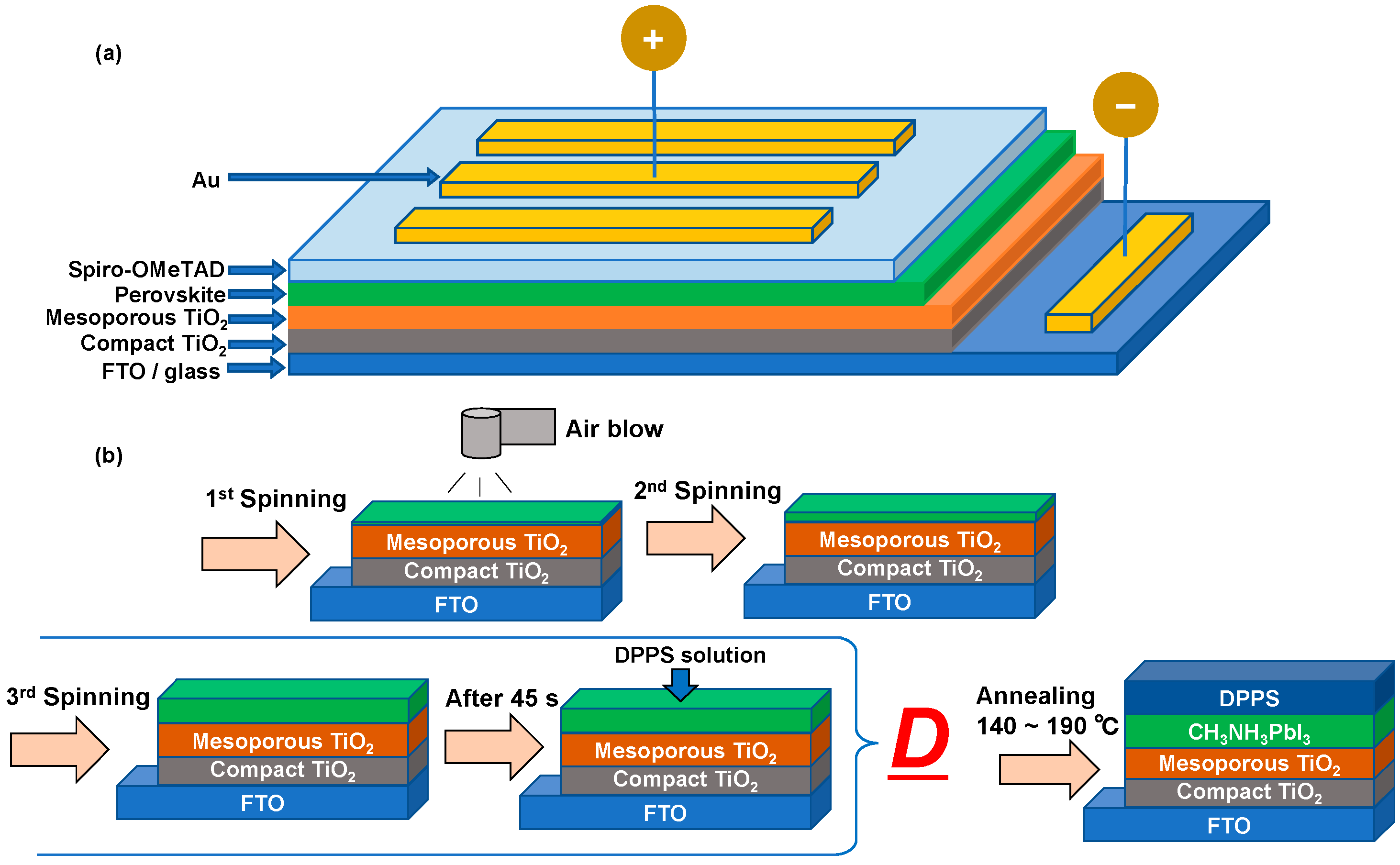
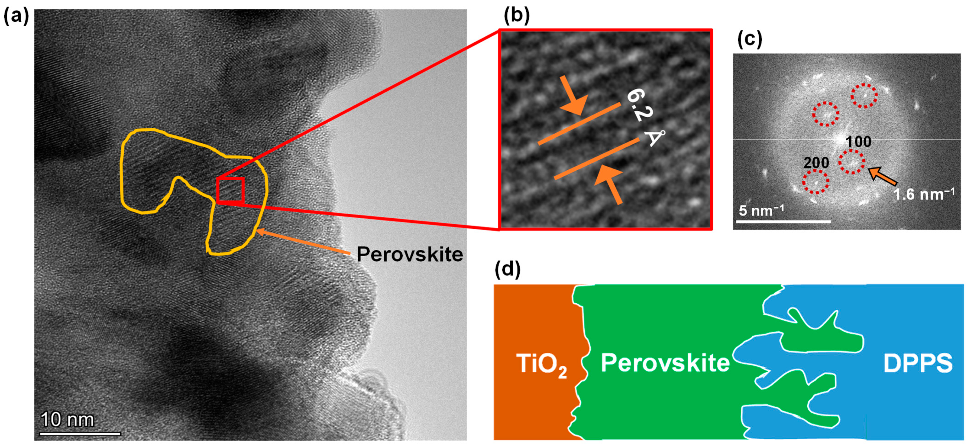
3. Results and Discussion
4. Conclusions
Author Contributions
Funding
Institutional Review Board Statement
Informed Consent Statement
Data Availability Statement
Conflicts of Interest
References
- Jiang, Q.; Zhang, L.; Wang, H.; Yang, X.; Meng, J.; Liu, H.; Yin, Z.; Wu, J.; Zhang, X.; You, J. Enhanced electron extraction using SnO2 for high-efficiency planar-structure HC(NH2)2PbI3-based perovskite solar cells. Nat. Energy 2017, 2, 16177. [Google Scholar] [CrossRef]
- Bi, E.; Chen, H.; Xie, F.; Wu, Y.; Chen, W.; Su, Y.; Islam, A.; Gratzel, M.; Yang, X.; Han, L. Diffusion engineering of ions and charge carriers for stable efficient perovskite solar cells. Nat. Commun. 2017, 8, 15330. [Google Scholar] [CrossRef]
- Han, Q.; Hsieh, Y.T.; Meng, L.; Wu, J.L.; Sun, P.; Yao, E.P.; Chang, S.Y.; Bae, S.H.; Kato, T.; Bermudez, V.; et al. High-performance perovskite/Cu(In,Ga)Se2monolithic tandem solar cells. Science 2018, 361, 904–908. [Google Scholar] [CrossRef] [PubMed]
- Mei, A.; Li, X.; Liu, L.; Ku, Z.; Liu, T.; Rong, Y.; Xu, M.; Hu, M.; Chen, J.; Yang, Y.; et al. A hole-conductor-free, fully printable mesoscopic perovskite solar cell with high stability. Science 2014, 345, 295–298. [Google Scholar] [CrossRef]
- Li, G.; Zhang, T.; Xu, F.; Zhao, Y. A facile deposition of large grain and phase pure α-FAPbI3 for perovskite solar cells via a flash crystallization. Mater. Today Energy 2017, 5, 293–298. [Google Scholar] [CrossRef]
- Oku, T. Crystal structures of perovskite halide compounds used for solar cells. Rev. Adv. Mater. Sci. 2020, 59, 264–305. [Google Scholar] [CrossRef]
- Ueoka, N.; Oku, T.; Suzuki, A. Effects of doping with Na, K, Rb, and formamidinium cations on (CH3NH3)0.99Rb0.01Pb0.99Cu0.01I3-x(Cl, Br)x perovskite photovoltaic cells. AIP Adv. 2020, 10, 125023. [Google Scholar] [CrossRef]
- Wu, Y.; Yang, X.; Chen, W.; Yue, Y.; Cai, M.; Xie, F.; Bi, E.; Islam, A.; Han, L. Perovskite solar cells with 18.21% efficiency and area over 1 cm2 fabricated by heterojunction engineering. Nat. Energy 2016, 1, 16148. [Google Scholar] [CrossRef]
- Guerra, V.L.P.; Altamura, D.; Trifiletti, V.; Colella, S.; Listorti, A.; Giannuzzi, R.; Pellegrino, G.; Condorelli, G.G.; Giannini, C.; Gigli, G.; et al. Implications of TiO2 surface functionalization on polycrystalline mixed halide perovskite films and photovoltaic devices. J. Mater. Chem. A 2015, 3, 20811–20818. [Google Scholar] [CrossRef]
- Suzuki, A.; Oe, M.; Oku, T. Fabrication and characterization of Ni-, Co-, and Rb-incorporated CH3NH3PbI3 perovskite solar cells. J. Electron. Mater. 2021, 50, 1980–1995. [Google Scholar] [CrossRef]
- Wang, R.; Mujahid, M.; Duan, Y.; Wang, Z.-K.; Xue, J.; Yang, Y. A review of perovskites solar cell stability. Adv. Funct. Mater. 2019, 29, 1808843. [Google Scholar] [CrossRef]
- Hou, X.; Huang, S.; Ou-Yang, W.; Pan, L.; Sun, Z.; Chen, X. Constructing efficient and stable perovskite solar cells via interconnecting perovskite grains. ACS Appl. Mater. Interfaces 2017, 9, 35200–35208. [Google Scholar] [CrossRef] [PubMed]
- Ueoka, N.; Oku, T. Effects of co-addition of sodium chloride and copper (II) bromide to mixed-cation mixed-halide perovskite photovoltaic devices. ACS Appl. Energy Mater. 2020, 3, 7272–7283. [Google Scholar] [CrossRef]
- Lee, J.W.; Kim, S.G.; Bae, S.H.; Lee, D.K.; Lin, O.; Yang, Y.; Park, N.G. The interplay between trap density and hysteresis in planar heterojunction perovskite solar cells. Nano Lett. 2017, 17, 4270–4276. [Google Scholar] [CrossRef]
- Berhe, T.A.; Su, W.-N.; Chen, C.-H.; Pan, C.-J.; Cheng, J.-H.; Chen, H.-M.; Tsai, M.-C.; Chen, L.-Y.; Dubale, A.A.; Hwang, B.-J. Organometal halide perovskite solar cells: Degradation and stability. Energy Environ. Sci. 2016, 9, 323–356. [Google Scholar] [CrossRef]
- Conings, B.; Drijkoningen, J.; Gauquelin, N.; Babayigit, A.; D’Haen, J.; D’Olieslaeger, L.; Ethirajan, A.; Verbeeck, J.; Manca, J.; Mosconi, E.; et al. Intrinsic thermal instability of methylammonium lead trihalide perovskite. Adv. Energy Mater. 2015, 5, 1500477. [Google Scholar] [CrossRef]
- Zhang, C.-C.; Li, M.; Wang, Z.-K.; Jiang, Y.-R.; Liu, H.-R.; Yang, Y.-G.; Gao, X.-Y.; Ma, H. Passivated perovskite crystallization and stability in organic-inorganic halide solar cells by doping a donor polymer. J. Mater. Chem. A 2017, 5, 2572–2579. [Google Scholar] [CrossRef]
- Zhao, Y.; Wei, J.; Li, H.; Yan, Y.; Zhou, W.; Yu, D.; Zhao, Q. A polymer scaffold for self-healing perovskite solar cells. Nat. Commun. 2016, 7, 10228. [Google Scholar] [CrossRef] [PubMed]
- Yang, W.S.; Park, B.W.; Jung, E.H.; Jeon, N.J.; Kim, Y.C.; Lee, D.U.; Shin, S.S.; Seo, J.; Kim, E.K.; Noh, J.H.; et al. Iodide management in formamidinium-lead-halide-based perovskite layers for efficient solar cells. Science 2017, 356, 1376–1379. [Google Scholar] [CrossRef]
- Lee, J.-W.; Dai, Z.; Lee, C.; Lee, H.M.; Han, T.-H.; De Marco, N.; Lin, O.; Choi, C.S.; Dunn, B.; Koh, J.; et al. Tuning molecular interactions for highly reproducible and efficient formamidinium perovskite solar cells via adduct approach. J. Am. Chem. Soc. 2018, 140, 6317–6324. [Google Scholar] [CrossRef]
- Jiang, J.; Wang, Q.; Jin, Z.; Zhang, X.; Lei, J.; Bin, H.; Zhang, Z.-G.; Li, Y.; Liu, S. Polymer doping for high-efficiency perovskite solar cells with improved moisture stability. Adv. Energy Mater. 2017, 8, 1701757. [Google Scholar] [CrossRef]
- Seo, S.; Jeong, S.; Bae, C.; Park, N.-G.; Shin, H. Perovskite solar cells with inorganic electron- and hole-transport layers exhibiting long-term (≈500 h) stability at 85 °C under continuous 1 sun illumination in ambient air. Adv. Mater. 2018, 30, e1801010. [Google Scholar] [CrossRef] [PubMed]
- Li, M.; Wang, Z.-K.; Kang, T.; Yang, Y.; Gao, X.; Hsu, C.-S.; Li, Y.; Liao, L.-S. Graphdiyne-modified cross-linkable fullerene as an efficient electron-transporting layer in organometal halide perovskite solar cells. Nano Energy 2018, 43, 47–54. [Google Scholar] [CrossRef]
- Chen, Q.; De Marco, N.; Yang, Y.; Song, T.-B.; Chen, C.-C.; Zhao, H.; Hong, Z.; Zhou, H.; Yang, Y. Under the spotlight: The organic-inorganic hybrid halide perovskite for optoelectronic applications. Nano Today 2015, 10, 355–396. [Google Scholar] [CrossRef]
- Xiang, W.; Chen, Q.; Wang, Y.; Liu, M.; Huang, F.; Bu, T.; Wang, T.; Cheng, Y.-B.; Gong, X.; Zhong, J.; et al. Improved air stability of perovskite hybrid solar cells via blending poly(dimethylsiloxane)-urea copolymers. J. Mater. Chem. A 2017, 5, 5486–5494. [Google Scholar] [CrossRef]
- Wang, K.; Zheng, L.; Zhu, T.; Liu, L.; Becker, M.L.; Gong, X. High performance perovskites solar cells by hybrid perovskites co-crystallized with poly(ethylene oxide). Nano Energy 2019, 67, 104229. [Google Scholar] [CrossRef]
- Han, T.-H.; Lee, J.-W.; Choi, C.; Tan, S.; Lee, C.; Zhao, Y.; Dai, Z.; De Marco, N.; Lee, S.-J.; Bae, S.-H.; et al. Perovskite-polymer composite cross-linker approach for highly-stable and efficient perovskite solar cells. Nat. Commun. 2019, 10, 520. [Google Scholar] [CrossRef]
- Wang, R.; Xue, J.; Meng, L.; Lee, J.; Zhao, Z.; Sun, P.; Cai, L.; Huang, T.; Wang, Z.; Wang, Z.K.; et al. Caffeine improves the performance and thermal stability of perovskite solar cells. Joule 2019, 3, 1464–1477. [Google Scholar] [CrossRef]
- Liu, L.; Huang, S.; Lu, Y.; Liu, P.; Zhao, Y.; Shi, C.; Zhang, S.; Wu, J.; Zhong, H.; Sui, M.; et al. Grain-Boundary “patches” by in situ conversion to enhance perovskite solar cells stability. Adv. Mater. 2018, 30, e1800544. [Google Scholar] [CrossRef]
- Lee, J.-W.; Dai, Z.; Han, T.-H.; Choi, C.; Chang, S.-Y.; Lee, S.-J.; De Marco, N.; Zhao, H.; Sun, P.; Huang, Y.; et al. 2D perovskite stabilized phase-pure formamidinium perovskite solar cells. Nat. Commun. 2018, 9, 3021. [Google Scholar] [CrossRef]
- Lee, J.W.; Bae, S.H.; Hsieh, Y.T.; De Marco, N.; Wang, M.; Sun, P.; Yang, Y. A bifunctional Lewis base additive for microscopic homogeneity in perovskite solar cells. Chem 2017, 3, 290–302. [Google Scholar] [CrossRef]
- Taguchi, M.; Suzuki, A.; Oku, T.; Fukunishi, S.; Minami, S.; Okita, M. Effects of decaphenylcyclopentasilane addition on photovoltaic properties of perovskite solar cells. Coatings 2018, 8, 461. [Google Scholar] [CrossRef]
- Oku, T.; Kandori, S.; Taguchi, M.; Suzuki, A.; Okita, M.; Minami, S.; Fukunishi, S.; Tachikawa, T. Polysilane-inserted methylammonium lead iodide perovskite solar cells doped with formamidinium and potassium. Energies 2020, 13, 4776. [Google Scholar] [CrossRef]
- Taguchi, M.; Suzuki, A.; Oku, T.; Ueoka, N.; Minami, S.; Okita, M. Effects of annealing temperature on decaphenylcyclopentasilane-inserted CH3NH3PbI3 perovskite solar cells. Chem. Phys. Lett. 2019, 737, 136822. [Google Scholar] [CrossRef]
- Oku, T.; Taguchi, M.; Suzuki, A.; Kitagawa, K.; Asakawa, Y.; Yoshida, S.; Okita, M.; Minami, S.; Fukunishi, S.; Tachikawa, T. Effects of polysilane addition to chlorobenzene and high temperature annealing on CH3NH3PbI3 perovskite photovoltaic devices. Coatings 2021, 11, 665. [Google Scholar] [CrossRef]
- Oku, T.; Nakagawa, J.; Iwase, M.; Kawashima, A.; Yoshida, K.; Suzuki, A.; Akiyama, T.; Tokumitsu, K.; Yamada, M.; Nakamura, M. Microstructures and photovoltaic properties of polysilane-based solar cells. Jpn. J. Appl. Phys. 2013, 52, 04CR07. [Google Scholar] [CrossRef]
- Oku, T.; Nomura, J.; Suzuki, A.; Tanaka, H.; Fukunishi, S.; Minami, S.; Tsukada, S. Fabrication and characterization of CH3NH3PbI3 perovskite solar cells added with polysilanes. Int. J. Photoenergy 2018, 2018, 8654963. [Google Scholar] [CrossRef]
- Suzuki, A.; Taguchi, M.; Oku, T.; Okita, M.; Minami, S.; Fukunishi, S.; Tachikawa, T. Additive effects of methyl ammonium bromide or formamidinium bromide in methylammonium lead iodide perovskite solar cells using decaphenylcyclopentasilane. J. Mater. Sci. Mater. Electron. 2021, 32, 26449–26464. [Google Scholar] [CrossRef]
- Oku, T.; Zushi, M.; Imanishi, Y.; Suzuki, A.; Suzuki, K. Microstructures and photovoltaic properties of perovskite-type CH3NH3PbI3 compounds. Appl. Phys. Express 2014, 7, 121601. [Google Scholar] [CrossRef]
- Kishimoto, T.; Oku, T.; Suzuki, A.; Ueoka, N. Additive effects of guanidinium iodide on CH3NH3PbI3 perovskite solar cells. Phys. Status Solidi A 2021, 218, 2100396. [Google Scholar] [CrossRef]
- Kandori, S.; Oku, T.; Nishi, K.; Kishimoto, T.; Ueoka, N.; Suzuki, A. Fabrication and characterization of potassium- and formamidinium-added perovskite solar cells. J. Ceram. Soc. Jpn. 2020, 128, 805–811. [Google Scholar] [CrossRef]
- Nishi, K.; Oku, T.; Kishimoto, T.; Ueoka, N.; Suzuki, A. Photovoltaic characteristics of CH3NH3PbI3 perovskite solar cells added with ethylammonium bromide and formamidinium iodide. Coatings 2020, 10, 410. [Google Scholar] [CrossRef]
- Machiba, H.; Oku, T.; Kishimoto, T.; Ueoka, N.; Suzuki, A. Fabrication and evaluation of K-doped MA0.8FA0.1K0.1PbI3(Cl) perovskite solar cells. Chem. Phys. Lett. 2019, 730, 117–123. [Google Scholar] [CrossRef]
- Oku, T.; Ohishi, Y.; Ueoka, N. Highly (100)-oriented CH3NH3PbI3(Cl) perovskite solar cells prepared with NH4Cl using an air blow method. RSC Adv. 2018, 8, 10389–10395. [Google Scholar] [CrossRef] [PubMed]
- Suzuki, A.; Kitagawa, K.; Oku, T.; Okita, M.; Fukunishi, S.; Tachikawa, T. Additive effects of copper and alkali metal halides into methylammonium lead iodide perovskite solar cells. Electron. Mater. Lett. 2022, 18, 176–186. [Google Scholar] [CrossRef]
- Ono, I.; Oku, T.; Suzuki, A.; Asakawa, Y.; Terada, S.; Okita, M.; Fukunishi, S.; Tachikawa, T. Fabrication and characterization of CH3NH3PbI3 solar cells with added guanidinium and inserted with decaphenylpentasilane. Jpn. J. Appl. Phys. 2022, 61, SB1024. [Google Scholar] [CrossRef]
- Okumura, R.; Oku, T.; Suzuki, A.; Okita, M.; Fukunishi, S.; Tachikawa, T.; Hasegawa, T. Effects of adding alkali metals and organic cations to Cu-based perovskite solar cells. Appl. Sci. 2022, 12, 1710. [Google Scholar] [CrossRef]
- Enomoto, A.; Suzuki, A.; Oku, T.; Okita, M.; Fukunishi, S.; Tachikawa, T.; Hasegawa, T. Effects of Cu, K and guanidinium addition to CH3NH3PbI3 perovskite solar cells. J. Electron. Mater. 2022, 51, 4317–4328. [Google Scholar] [CrossRef]

| Devices | JSC (mA cm−2) | VOC (V) | FF | RS (Ω cm−2) | RSh (Ω cm−2) | η (%) | ηave (%) |
|---|---|---|---|---|---|---|---|
| Standard | 18.9 | 0.844 | 0.410 | 5.90 | 85.3 | 6.55 | 5.19 |
| D × 1 | 17.0 | 0.846 | 0.443 | 5.07 | 110 | 6.38 | 5.65 |
| D × 2 | 21.3 | 0.696 | 0.466 | 8.38 | 290 | 6.89 | 5.36 |
| D × 3 | 23.2 | 0.771 | 0.620 | 5.59 | 2100 | 11.09 | 9.19 |
| D × 4 | 17.3 | 0.877 | 0.493 | 7.21 | 124 | 7.50 | 5.96 |
| Time (Day) | JSC (mA cm−2) | VOC (V) | FF | RS (Ω cm−2) | RSh (Ω cm−2) | η (%) | ηave (%) |
|---|---|---|---|---|---|---|---|
| As-prepared | 23.2 | 0.771 | 0.620 | 5.59 | 2100 | 11.09 | 9.19 |
| 149 days | 18.6 | 0.862 | 0.707 | 4.54 | 842 | 11.38 | 9.46 |
| 191 days | 21.4 | 0.887 | 0.701 | 5.17 | 1840 | 13.33 | 11.22 |
| 226 days | 19.3 | 0.893 | 0.701 | 5.99 | 1410 | 12.10 | 10.40 |
Publisher’s Note: MDPI stays neutral with regard to jurisdictional claims in published maps and institutional affiliations. |
© 2022 by the authors. Licensee MDPI, Basel, Switzerland. This article is an open access article distributed under the terms and conditions of the Creative Commons Attribution (CC BY) license (https://creativecommons.org/licenses/by/4.0/).
Share and Cite
Mizuno, S.; Oku, T.; Suzuki, A.; Okita, M.; Fukunishi, S.; Tachikawa, T.; Hasegawa, T. Photovoltaic Properties and Microstructures of Polysilane-Added Perovskite Solar Cells. Chem. Proc. 2022, 9, 20. https://doi.org/10.3390/IOCC_2022-12169
Mizuno S, Oku T, Suzuki A, Okita M, Fukunishi S, Tachikawa T, Hasegawa T. Photovoltaic Properties and Microstructures of Polysilane-Added Perovskite Solar Cells. Chemistry Proceedings. 2022; 9(1):20. https://doi.org/10.3390/IOCC_2022-12169
Chicago/Turabian StyleMizuno, Shinichiro, Takeo Oku, Atsushi Suzuki, Masanobu Okita, Sakiko Fukunishi, Tomoharu Tachikawa, and Tomoya Hasegawa. 2022. "Photovoltaic Properties and Microstructures of Polysilane-Added Perovskite Solar Cells" Chemistry Proceedings 9, no. 1: 20. https://doi.org/10.3390/IOCC_2022-12169
APA StyleMizuno, S., Oku, T., Suzuki, A., Okita, M., Fukunishi, S., Tachikawa, T., & Hasegawa, T. (2022). Photovoltaic Properties and Microstructures of Polysilane-Added Perovskite Solar Cells. Chemistry Proceedings, 9(1), 20. https://doi.org/10.3390/IOCC_2022-12169