Proceeding Paper

First Principles Investigation of the Optoelectronic Properties of Molybdenum Dinitride for Optical Sensing Applications †

by
Amall A. Ramanathan
Department of Physics, The University of Jordan, Amman 11942, Jordan
Presented at the 1st International Electronic Conference on Chemical Sensors and Analytical Chemistry, 1–15 July 2021; Available online: https://csac2021.sciforum.net/.
Chem. Proc. 2021, 5(1), 27; https://doi.org/10.3390/CSAC2021-10429
Published: 30 June 2021

Abstract

:
The electronic and optical properties of the newly synthesized molybdenum dinitride (MoN2) in the hypothetical 2H structure analogous to MoS2 is investigated using the density functional theory (DFT) full potential linearized augmented plane wave (FP-LAPW) method and the modified Becke–Johnson (mBJ) approximation. The aim is to investigate the optoelectronic properties of this compound for potential optical sensing applications and compare with the capabilities of MoS2 in this field. As compared to MoS2, which is a semiconductor, MoN2 is found to be a semi metal from the band structure plots. The dielectric function, optical conductivity and the optical constants, namely, the refractive index, the reflectivity, the extinction and absorption coefficients, are evaluated and compared with those of MoS2 and discussed with reference to the sensing performance.

1. Introduction

The high potential of transition metal dichalcogenides (TMD) for electronic, sensing, photonic and thermoelectric device applications has been exploited this past decade, and especially MoS2, a prototype TMD material, has shown a lot of promise [1,2,3]. It has been studied and characterized extensively for structural, electronic, optical and transport properties both in bulk and in the 2D limit [4,5,6]. Interest in TM nitrides has been rekindled because they exhibit a number of unique and advanced catalytic properties for photo and electrochemical catalysis [7,8]. There were no layered structures in any of these studies. Layered structures provide more flexibility in doping, the ease of going down to lower dimensions and materials design.
The search for layered nitrogen rich TM nitrides, particularly those of the MoS2 type, led to the recent synthesis and discovery of 3R-MoN2, which has the rhombohedral MoS2 structure [9]. It was synthesized through a high P-T route of solid-state ion exchange and has shown great potential for applications in catalysis and hydrogenation. In addition, the very recent first principle study of MoN2 monolayer by Zhang et al. [10] showed the 1H configuration to be the most stable among the structures considered in their study. Their study revealed the importance of 2D MoN2 as a high-capacity electrode material for metal ion batteries. Further, the first principles study of Ramanathan and Khalifeh [11] has shown the 2H MoN2 to be a promising thermoelectric material.
All the above interesting results for MoN2 provide a strong motivation to study this compound. Considering that to date no optical characterization of MoN2 has been performed, the present study is devoted to the determination of the electronic and optical properties from first principles and to look at the various possibilities for optical sensing applications of MoN2. Since an optical sensor measures a physical property of light and, depending upon the sensor usage, converts it to a readable output, it is highly essential to characterize the optical properties of the new layered material MoN2. The hypothetical 2H structure analogous to MoS2 of MoN2 is investigated using the DFT full potential linearized augmented plane wave (FP-LAPW) method and the mBJ approximation. In addition, the 2H MoS2 optoelectronic properties are determined by the same method for the sake of completeness and comparison.

2. Calculation Details

The geometry of MoN2 is optimized using the ABINIT software program [12,13] with the generalized gradient approximation (GGA) of Perdew, Burke and Ernzerhof (PBE) PAW (projector augmented wave) pseudopotentials [14]. All the structural calculations are performed with convergence criteria of less than 1 × 10⁻⁶ Ha for the self-consistent field (SCF) iterations and a threshold of less than 1 mRy/a.u. for the optimization of the geometries [15,16]. The fully relaxed MoS2 lattice constant values are taken from our previous work [6].
The optimized structures and lattice constant values are then used with the WIEN2k [17] code to perform full-potential linearized-augmented plane wave (FP-LAPW) calculation employing GGA_PBE to obtain the ground state energy and electronic properties at a 20 × 20 × 4 k-point grid. The optical properties are evaluated using denser grids of 40 × 40 × 5 with the more accurate mBJ exchange correlation of Trans Blaha (TB-mBJ) [18].

3. Results and Discussion

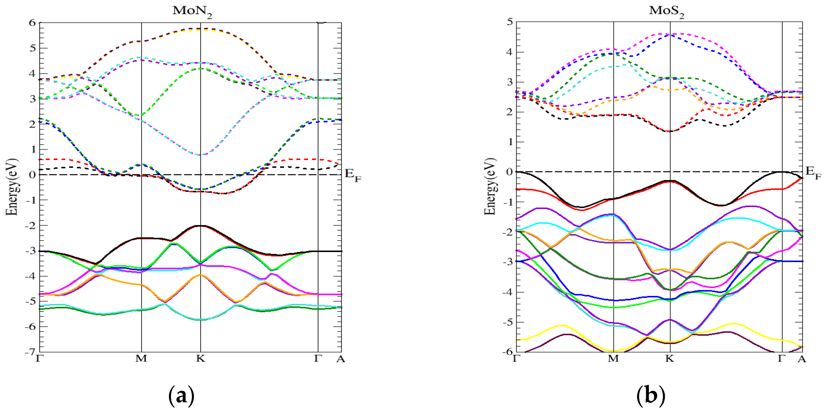
3.1. Structural and Electronic

The 2H-MoN2/MoS2 unit cells have hexagonal symmetry and consist of two stacks of three atomic layers; each stack consists of a Mo atomic plane sandwiched between two N/S atomic planes respectively. The atoms are bonded covalently in plane and the stacks are held together by weak Van der Waals force.
The non-magnetic state is the ground state for both the layered compounds and the structural relaxation of the system with a complete relaxation of all the atoms which simultaneously gives us the equilibrium geometry. The lattice parameter a and c values of MoN2 are 3.094 and 11.975 Å, respectively. The lattice parameter values of MoN2 are much smaller than that of MoS2 due to the shorter bond lengths of Mo–N as compared to Mo–S. The lattice parameters for MoS2 a = 3.193 and c = 12.359 Å taken from previous work [6] using the LDA (local density approximation) are in good agreement with the experimental values [19] aexp = 3.16 Å and cexp = 12.29 Å and within 2.3 and 0.6%, respectively.
The equilibrium lattice constant values for MoN2 and MoS2 are used with the GGA-PBE WIEN2k code to extract the electronic band structures with a 20 × 20 × 4 k-point grid.
We notice that there is a change in the electronic distribution of MoN2 as compared to MoS2 which is reflected in the band structure of MoN2, as shown in Figure 1. The MoS2 band structure is also shown on the right panel of Figure 1. The band structures illustrate the change in behavior of MoN2 to a semi metal one from the semiconducting one of MoS2. There is an overlap between the bottom of the conduction band and the top of the valence band in MoN2. This semi-metal feature implies that there is a range of energies for which electrons and holes co-exist. The Mo 4d, S 3p and N 2p atomic orbitals play a decisive role in the band structure properties as shown by the total and partial density of states plots Figures S1 and S2 (a and b).

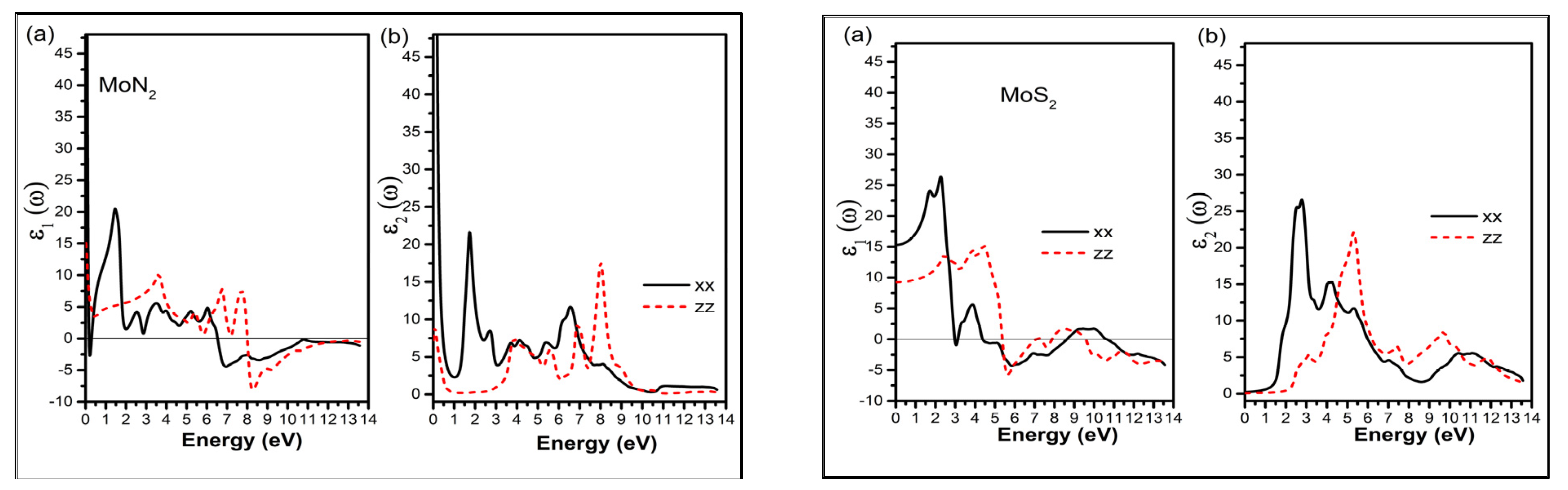
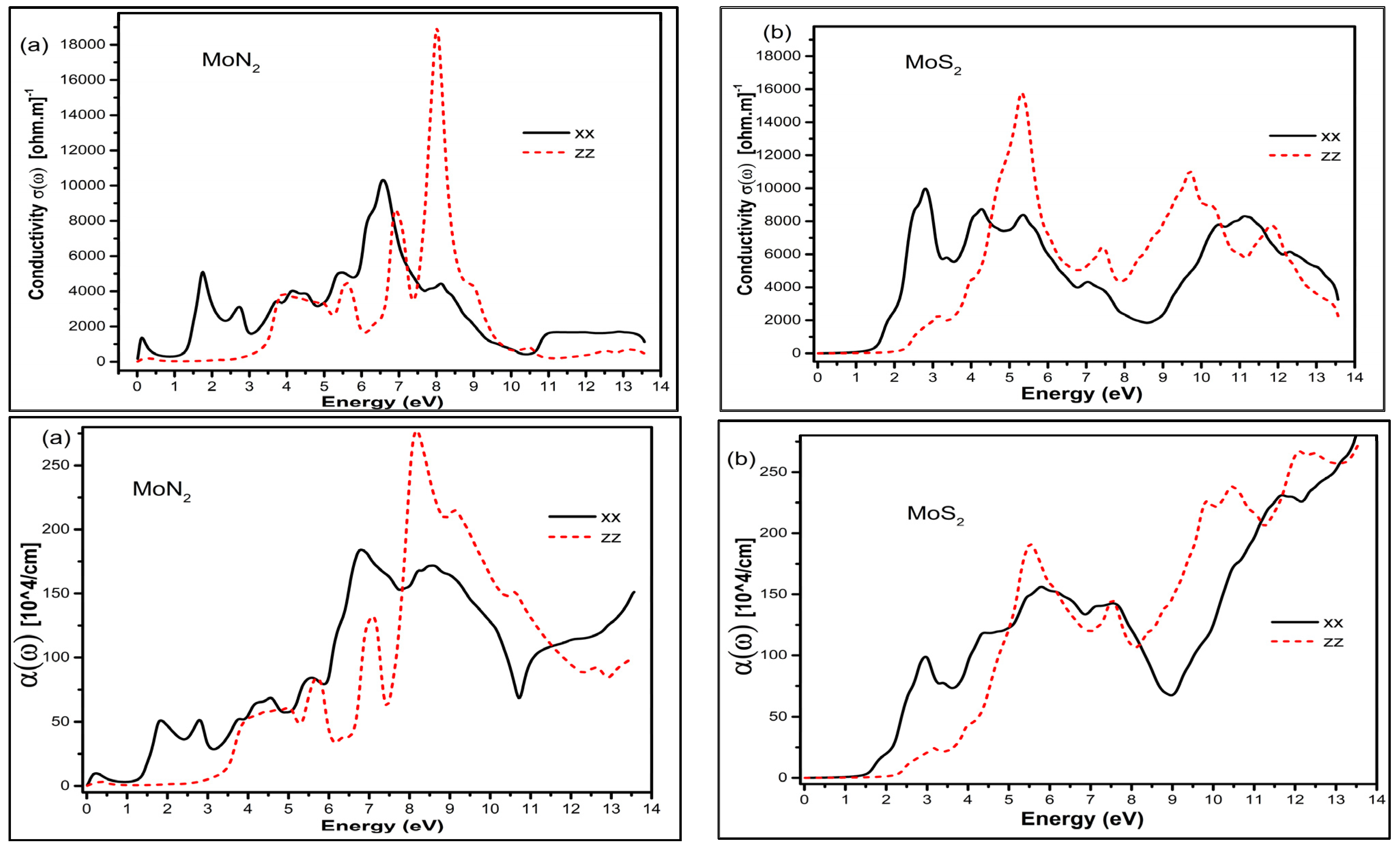
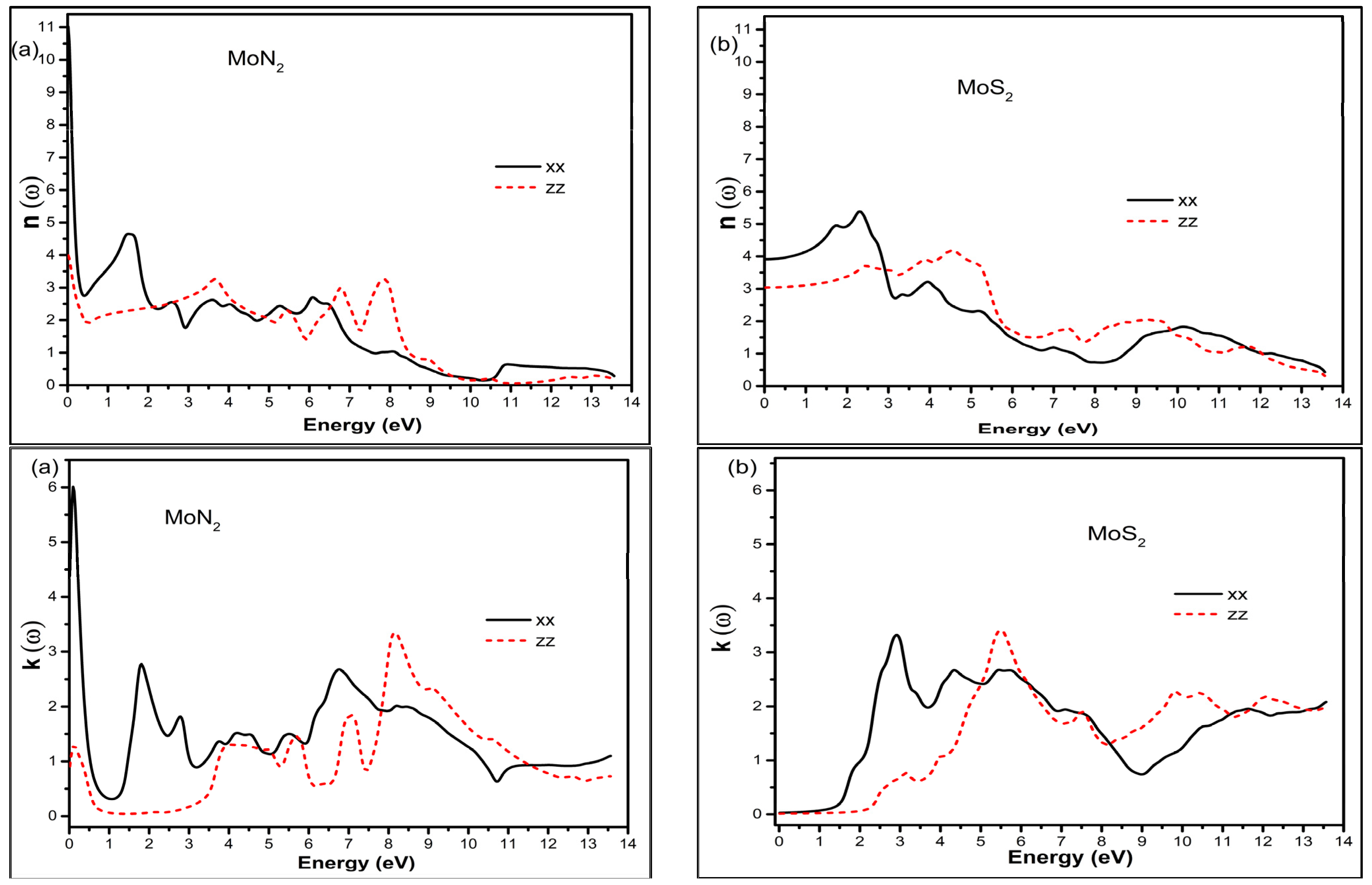
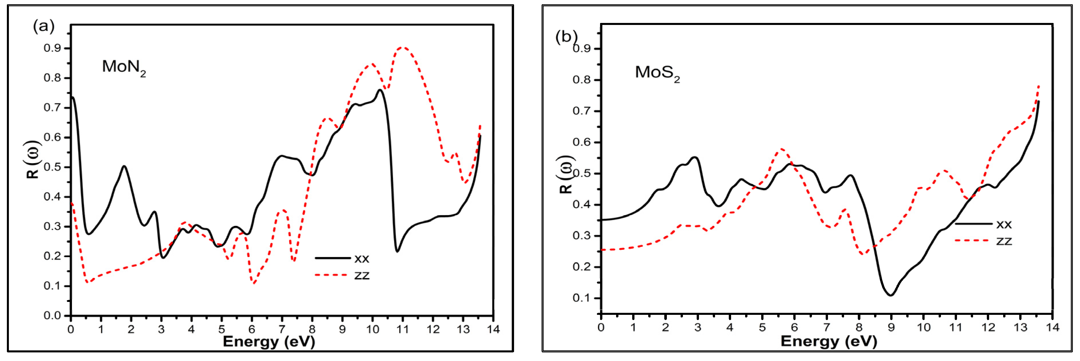
3.2. Optical Properties

The TB-mBJ proves to be an excellent choice with a 40 × 40 × 5 grid for calculating the optical properties with a high degree of accuracy for MoN2 and MoS2. This section is devoted to the presentation and discussion of the results for the dielectric function and optical conductivity. In addition, the optical constants, namely, the refractive index, the reflectivity, the extinction and absorption coefficients, are obtained and interpreted.
The complex dielectric function (ε = ε1 + iε2) is a function of the amount of light absorbed by the material. The imaginary part of dielectric function, ε2 (ω), which represents absorption behavior, can be calculated from the electronic band structure of solids. The real part of dielectric function, ε1 (ω), which represents the electronic polarization under incident light can be calculated according to Kramers–Kroing relation [20,21]. Figure 2 shows the real and imaginary plots for the dielectric function for MoN2 and MoS2 in the photon energy range of 0–14 eV. We see from the plots the anisotropy of the dielectric function. The general trend is the in-plane values are almost double that of the out-of-plane direction and the peaks for the zz direction are shifted more towards the right, towards higher photon energies. The dielectric plots show the high capability for absorption in the visible part of the spectrum for the in-plane direction and ultra-violet (UV) for the perpendicular direction, thereby effectively covering a wide range of energies.
The complex index of refraction of the medium N is defined as N = ε = n + i k , where n is the refractive index and k the extinction coefficient. These are depicted in Figure 3.
Once again, we see the anisotropy in the two directions for these optical constants. The amplitudes in the xx direction are larger and closer to the visible range for both the n (ω) and k (ω) compounds. We notice that MoN2 has large static (ω = 0) refractive index values of ~11 and 4 in the xx and zz directions, respectively. In contrast the corresponding values for MoS2 are 4 and 3. The larger values of n (ω) imply higher electron density. In contrast to MoS2, MoN2 has peak extinction coefficient values at ω = 0 of 4.4 and 0.9 in the xx and zz directions, respectively. Both MoN2 and MoS2 show low k (ω) values in the infrared and MoS2 continues to have almost zero values up to 1.5 and 2.5 eV for the xx and zz directions, respectively. The first maxims of MoS2 are at 3 eV of the spectra and the magnitude in the xx direction is almost six times larger than in the zz direction. The second k peak for the zz direction is in the UV region and slightly larger than the first xx peak. Since the extinction coefficient reflects the degree to which light is absorbed, we can see that the in-plane direction is most favorable for both compounds. However, in contrast to MoS2, with MoN2 we have strong absorption in infrared in addition to the visible region of the photon energy.
The conductivity and absorption coefficient graphs for MoN2 and MoS2 are shown in Figure 4. The graphs show for the xx in-plane direction maximum conductivity is in the UV region for MoN2 whereas for MoS2 it is in the visible part of the photon energy. The conductivity in the zz direction has peak positions in the UV region around 8 and 5 eV for MoN2 and MoS2, respectively.
The absorption on the other hand shows the first peak in the visible and second broader peak with a much higher magnitude in the UV region for MoN2; and a very broad peak of almost constant magnitude for MoS2, covering the visible and the UV region in the in-plane xx direction. Beyond 10 eV, both MoN2 and MoS2 show a rise in the absorption coefficient. With respect to the zz direction, there are a set of small peaks beyond the visible and a sharp maximum value peak at around 9 eV of the UV region for MoN2; whereas for MoS2, the peaks are around 6, 10 and 12 eV in the UV region. These characteristics confirm the suitability of MoN2 and MoS2 for visible and UV sensing applications. The reflectance is depicted in Figure 5 and we observe large static reflectance value greater than 0.7 for MoN2 that is double that of MoS2 in the xx direction. In the zz direction, the values are 0.35 and 0.25 for MoN2 and MoS2 respectively. The graphs show that MoN2 is a good infrared reflector, whereas MoS2 reflects best just beyond the visible range.

4. Conclusions

In conclusion, as opposed to MoS2, MoN2 is a semi metal as evinced from the band structure plots. Both the layered materials show anisotropy for all the optical properties with different magnitudes and peak positions, although the shapes of the graphs for the same property are similar in the two directions.
The large values of refractive index and good optical conductivity, absorption and reflectance results obtained reinstate the suitability of these materials for optical sensing applications. In comparison to MoS2, MoN2 shows suitability for infrared sensing applications in addition to visible and UV.

Supplementary Materials

The following are available online at https://www.mdpi.com/article/10.3390/CSAC2021-10429/s1.

Funding

No funding was received for this research work.

Institutional Review Board Statement

Not applicable.

Informed Consent Statement

Not applicable.

Data Availability Statement

Data can be provided upon reasonable request.

Conflicts of Interest

There are no conflict of interest to declare.

References

  1. Onofrio, N.; Guzman, D.M.; Strachan, A. Novel doping alternatives for transition metal dichalcogenides from high-throughput DFT calculations. J. Appl. Phys. 2017, 122, 185102. [Google Scholar] [CrossRef] [Green Version]
  2. Wang, Y.H.; Huang, K.J.; Wu, X. Recent advances in transition-metal dichalcogenides based electrochemical biosensors: A review. Biosens. Bioelectron. 2017, 97, 305. [Google Scholar] [CrossRef]
  3. Vikraman, D.; Akbar, K.; Hussain, S.; Yoo, G.; Jang, J.-Y.; Chun, S.-H.; Jung, J.; Park, H.J. Direct synthesis of thickness-tunable MoS2 quantum dot thin layers: Optical, structural and electrical properties and their application to hydrogen evolution. Nano Energy 2017, 35, 101. [Google Scholar] [CrossRef]
  4. Ramanathan, A.A. Defect Functionalization of MoS2 nanostructures as toxic gas sensors. IOP Conf. Ser. Mater. Sci. Eng. 2018, 305, 012001. [Google Scholar] [CrossRef] [Green Version]
  5. Zhang, H.; Lu, S.B.; Zheng, J.; Du, J.; Wen, S.C.; Tang, D.Y.; Loh, K.P. Molybdenum disulfide (MoS2) as a broadband saturable absorber for ultra-fast photonics. Opt. Express 2014, 22, 7249–7260. [Google Scholar] [CrossRef]
  6. Ramanathan, A.A.; Khalifeh, J.M. Enhanced thermoelectric properties of suspended mono and bilayer of MoS2 from first principles. IEEE Trans. Nanotechnol. 2018, 17, 974. [Google Scholar] [CrossRef]
  7. Chen, W.-F.; Muckerman, J.T.; Fujita, E. Recent developments in transition metal carbides and nitrides as hydrogen evolution electrocatalysts. Chem. Commun. 2013, 49, 8896–8909. [Google Scholar] [CrossRef] [PubMed]
  8. Tabata, M.; Maeda, K.; Higashi, M.; Lu, D.; Takata, T.; Abe, R.; Domen, K. Modified Ta3N5 powder as a photocatalyst for O2 evolution in a two-step water splitting system with an iodate/iodide shuttle redox mediator under visible light. Langmuir 2010, 26, 9161–9165. [Google Scholar] [CrossRef] [PubMed]
  9. Wang, S.M.; Ge, H.; Sun, S.L.; Zhang, J.Z.; Liu, F.M.; Wen, X.D.; Yu, X.H.; Wang, L.P.; Zhang, Y.; Xu, H.W.; et al. A New Molybdenum Nitride Catalyst with Rhombohedral MoS2 Structure for Hydrogenation Applications. J. Am. Chem. Soc. 2015, 137, 4815. [Google Scholar] [CrossRef] [PubMed]
  10. Zhang, X.; Yao, Y.; Yu, Z.; Wang, S.-S.; Guan, S.; Yang, H.Y.; Yang, S.A. Theoretical prediction of MoN2 monolayer as a high capacity electrode material for metal ion batteries. J. Mater. Chem. A 2016, 4, 15224. [Google Scholar] [CrossRef] [Green Version]
  11. Ramanathan, A.A.; Khalfeh, J.M. Thermoelectrics of MoS2(1−x)N2x Compounds. Phys. Sci. Biophys. J. 2021, 5, 000167. [Google Scholar] [CrossRef]
  12. Ramanathan, A.A. A DFT calculation of Nb and Ta (001) Surface Properties. J. Mod. Phys. 2013, 4, 432–437. [Google Scholar] [CrossRef] [Green Version]
  13. Gonze, X.; Jollet, F.; Araujo, F.A.; Adams, D.; Amadon, B.; Applencourt, T.; Audouze, C.; Beuken, J.M.; Bieder, J.; Bokhanchuk, A. Recent developments in the ABINIT software package. Comput. Phys. Commun. 2016, 205, 106. [Google Scholar] [CrossRef] [Green Version]
  14. Perdew, J.P.; Burke, K.; Ernzerhof, M. Generalized Gradient Approximation Made Simple. Phys. Rev. Lett. 1996, 77, 3865. [Google Scholar] [CrossRef] [Green Version]
  15. Ramanathan, A.A.; Khalifeh, J.M. Substrate matters: Magnetic tuning of the Fe monolayer. J. Magn. Magn. Mater. 2017, 426, 450–453. [Google Scholar] [CrossRef]
  16. Ramanathan, A.A.; Khalifeh, J.M.; Hamad, B.A. Evidence of surface magnetism in the V/Nb(0 0 1) system: A total energy pseudopotential calculation. Surf. Sci. 2008, 602, 607–613. [Google Scholar] [CrossRef]
  17. Blaha, P.; Schwarz, K.; Tran, F.; Laskowski, R.; Madsen, G.K.H.; Marks, L.D. WIEN2k: An APW+lo program for calculating the properties of solids. J. Chem. Phys. 2020, 152, 074101. [Google Scholar] [CrossRef]
  18. Tran, F.; Blaha, P. Accurate band gaps of semiconductors and insulators with a semilocal exchange-correlation potential. Phys. Rev. Lett. 2009, 102, 226401. [Google Scholar] [CrossRef] [PubMed] [Green Version]
  19. Coehoorn, R.; Haas, C.; Dijkstra, J.; Flipse, C.J.F.; de Groot, R.A.; Wold, A. Electronic structure of MoSe2, MoS2, and WSe2. I. Band-structure calculations and photoelectron spectroscopy. Phys. Rev. B 1987, 35, 6195. [Google Scholar] [CrossRef] [Green Version]
  20. Hulthén, R. Kramers–Kronig relations generalized: On dispersion relations for finite frequency intervals. A spectrum-restoring filter. J. Opt. Soc. Am. 1982, 72, 794–803. [Google Scholar] [CrossRef]
  21. Ramanathan, A.A.; Khalifeh, J.M. Electronic, magnetic and optical properties of XScO3 (X = Mo, W) perovskites. PeerJ Mater. Sci. 2021, 3, e15. [Google Scholar] [CrossRef]
Figure 1. The band structures of (a) MoN2 and (b) MoS2.
Chemproc 05 00027 g001
Figure 2. The dielectric function left panel MoN2 and right panel MoS2; (a) the real ε1 (ω) and (b) imaginary part ε2 (ω) for the in-plane (xx) and out of plane (zz) directions.
Chemproc 05 00027 g002
Figure 3. The refractive index top panel and extinction coefficient bottom panel for MoN2 (a) and MoS2 (b) in the xx in-plane and zz out of plane directions.
Chemproc 05 00027 g003
Figure 4. The optical conductivity top panel and absorption coefficient bottom panel for MoN2 (a) and MoS2 (b) in the xx in-plane and zz out of plane directions.
Chemproc 05 00027 g004
Figure 5. The reflectance R (ω) for MoN2 (a) and MoS2 (b) in the xx in-plane and zz out of plane directions in the photon energy range of 0–14 eV.
Chemproc 05 00027 g005
Publisher’s Note: MDPI stays neutral with regard to jurisdictional claims in published maps and institutional affiliations.

