Abstract
The exigency for continuous use of electrical devices has created greater demands for electricity along with more efficient transmission techniques. Energy from natural resources can be solar, thermal, vibration, friction, or Radio Frequencies (RF) signals. This state-of-the-art work provides a summary of RF energy harvesting techniques and can be used as a guide for the manufacture of RF energy scavenging modules. The use of Radio Frequency (RF) Energy Harvesting (EH) technique contributes to the development of autonomous energy devices and sensors. A rectenna system includes three main units: the receiving antenna, the impedance matching network, and the rectifier. We thoroughly analyze how to design a rectenna system with special emphasis given on the design of the rectifier. At the same time many works of the last 10 years are presented. This review article categorizes the used topologies depending on the type of antennas, IMNs, and rectifiers and comparatively presents their advantages and disadvantages.
1. Introduction
Energy harvesting (EH) is the process in which energy is harvested from the environment and converted into electrical power. The aim of energy harvesting is the energy autonomy of systems that would normally use batteries or were connected to a power supply network. This can be achieved by designing autonomous energy systems that can function in a variety of applications, such as in the diagnostic and therapeutical field (medical implants) with very low power consumption. Energy from the natural resources can be solar, thermal, vibration, friction, or Radio Frequencies (RF) signals and behave differently over time, depending on the operating environment of the system. In this work, we focus on RF Energy Harvesting and wireless power transfer (WPT techniques as potential sources in autonomous energy systems) [1].
Τhere are two different approaches of energy transfer: the dedicated transfer that means high power values or the harvesting of ambient energy that means low power values [2]. A circuit that harvests RF energy, from a dedicated source at a short-range is expected to produce power levels in the 50 nW/cm2 range. An example is an RFID chip that is powered by an RFID reader. The dedicated source enables embedded devices to recharge batteries. On the other hand, a circuit that harvests RF energy from an ambient source, can exploit this energy to charge various storage systems. This type of circuit is expected to produce power levels in the 2 nW/cm2 range. Typical ambient sources include Wi-Fi, GSM/Cellular, FM/TV/DTV, Bluetooth, etc. This type of source is common for applications for which is very difficult or impossible to replace batteries [3]. RF energy scavenging circuits are known for more than 60 years, but only a few have been able to harvest energy from ambient RF sources [4].
Maxwell formulated the first theoretical knowledge about wireless power transfer in 1864. Almost two centuries ago Nikola Tesla described how to transfer energy between two points without the need for a physical connection to a power source as “all-surpassing importance to man”. Hence the idea of wireless power transfer (WPT) has been around since the inception of electricity [5]. William C. Brown in the 1960s with the development of wireless communication technologies developed a rectifying antenna named “rectenna”. As a follow-up to this invention, his team conducted several experiments in 1968 on the transmission of microwave power, which were successful [6]. Figure 1 illustrates a typical RF energy harvesting system that consists of a transmission antenna and a rectenna that is comprised of receiving antenna, an impedance matching network (IMN), a rectifier, and a power management circuit. From all the parts of the rectenna, we discuss in detail about the synthesis of the rectifier. The challenge, during the design of a low input power rectifier, is the combination of a high output voltage and a high power conversion efficiency.
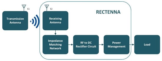
Figure 1.
Block diagram of a typical RF harvesting system.
The remainder of this review work is structured as follows. Firstly, the details and the parameters of the review process, as well as our contribution to this research topic are introduced in Section 2. In Section 3, a detailed analysis of the rectenna parts is performed and their qualitative and quantitative characteristics are described. Section 4 discusses the main results and remarks of this review work. Finally, Section 5 outlines the concluding remarks of this work.
2. Materials and Methods
During the last years, the RF energy harvesting and the design of rectenna systems are gaining popularity and have attracted the attention of several researchers. A bibliographic search using the keyword “RF energy harvesting” in the Scopus database shows that there are 1893 conference papers and 1442 journal papers related to RF energy harvesting from 2010 to 2020. Figure 2 displays the number of papers related to RF energy harvesting for the last 10 years. The purpose of this work is to describe in-depth the design process of a rectenna system and to present selected recent works about this scientific topic. Note that we emphasize on the design of the rectifier circuit. In this state-of-the-art work, we mention the most relevant works that had in their title the keywords “RF energy harvesting “or “RF to DC rectifier “or “DTMOS RF energy harvesting” and were published within the last 10 years.
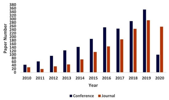
Figure 2.
Papers referring to RF energy harvesting from 2010 until 2020.
At first, we introduce few works that are categorized according to the type of receiving antenna. It should be noted that the antennas will not be analyzed in depth but we will only mention some basic designs, because such an analysis is out of the scope of this work. Then we present many works that are divided depending on the type of diode, the topology of the impedance matching network, and the topology of the rectifier circuit. We mention the pros and cons of each topology for both rectifiers and impedance matching networks. Presenting these works in this way, we aim to provide a detailed guide for the process of the rectenna design.
3. Results
3.1. Design Methology
The design methodology includes 4 steps:
- The procedure of choosing the right energy harvesting circuit topology.
- The selection process of a suitable diode.
- The design of an appropriate impedance matching network.
- The design, the optimization, and the simulation of the whole system [7].
Figure 3 illustrate this process.

Figure 3.
Block diagram of the design methodology in a rectenna system.
3.2. Design Specification
As it was mentioned in the introduction, a rectenna (rectifying antenna) is a combination of a jointly working antenna and an RF-to-DC rectifier. The antenna captures the RF electromagnetic energy, while the rectifier converts the input AC voltage into DC voltage, that can be used for low-power battery-operated devices. Additionally, another component between the RF-to-DC rectifier and the antenna is included, which is an impedance matching network and whose function is to adjust the impedance between these two elements. In this application, the input is the free space, while the output is the antenna port connected to the rest of the harvesting circuit.
3.2.1. Receiving Antenna
The main function of the receiving antenna is to scavenge as much RF radiation-power as possible. The main factors that are taken into account in its design are the reflected power at the input of the antenna, the impedance, the gain, and the antenna efficiency, as well as its weight and size. Several types exist in antenna design and various materials are utilized. The most common types are Bowtie antennas [8,9], log-periodic dipole arrays [10], dipole antennas [11], monopole antennas [12], loop antennas [13,14], Yagi-Uda antennas [15,16,17], planar inverted-F antennas [18], dielectric resonator antennas (DRAs) [19], etc. One of the most famous type of antennas for RF EH is the microstrip antennas, due to their comparative advantages [20,21,22,23].
In [8] we can find a broadband bowtie antenna, which operates as an energy harvester at 845 MHz and 3.5 GHz. The authors in [9] designed a modified printed bowtie antenna, operating in the frequency band of 5G NR mobile commutation networks. The log-periodic antenna in [10] was manufactured to harvest energy from six bands within the frequency range of 650 MHz to 2500 MHz. A compact rectenna with RF-based energy harvesting for IoT smart sensors is presented in [11]. The antenna of this system is a dipole antenna that operates in the range 902 MHz to 928 MHz. In [12] we can find a monopole antenna for ambient RF energy harvesting at the 600–1500 MHz band. The authors in [13] designed a loop antenna for RF energy harvesting at GSM-1800 band. Another loop antenna that operates at dual bands is described in [14]. The authors in [15] manufactured a rectenna using a Yagi-Uda antenna that can harvest RF power of GSM-1800 and UMTS-2100 bands. In [16,17] we can also find systems that use Yagi-Uda antennas. The first system operates at 2.45 GHz and the second at GSM-900 and GSM-1800 frequency bands. The authors in [18] designed a planar inverted-F antenna operating in the frequency bands GSM-900, GSM-1800. In [19] a dielectric resonator antenna is presented, which operates as an energy scavenger in the frequency band from 1.67 GHz to 6.7 GHz. The authors in [20] designed a differential microstrip antenna for the GSM900 band (890–960 MHz). Stacking two single-port patch antennas back to back gives us a compact dual-port L-probe patch antenna [21]. The measurement results show that there is an efficiency greater than 40% for the whole rectenna. In [22] we can find a dual-band E-shaped (modified) patch antenna, which operates as an energy scavenger at the frequency bands of two different systems; Narrow-band Internet of Things (NB-IoT) and EGSM-900 Mobile Communication Systems. Also, the same authors in [23] designed, optimized, and fabricated a multiband patch antenna that was operating in the frequency bands of LoRaWAN, GSM-1800 UMTS-2100. The proposed antenna showed acceptable performance for RF energy harvesting applications. Table 1 summarizes different types of antennas that have been utilized in RF energy harvesting systems.

Table 1.
Type of antennas that have been applied in RF energy harvesting systems.
3.2.2. Impedance Matching Network
The design of an impedance matching network is indispensable for the design of the rectenna because when the impedance of the rectifier does not match the impedance of the antenna, a percentage of the power from the source is not absorbed and is reflected in the environment. Therefore, the impedance of the antenna and the rectifier must be matched at the desired operating frequency so that the impedances are complex conjugates of each other [24]. An ideal circuit of this type for RF energy scavenging must not only provide the desired impedance matching between the antenna and rectifier but must further do so with minimum losses so that the amount harvested can be maximized [25].
The complex source impedance (RSource + jXSource) has to be matched with the load impedance (RLoad + j0). This can be achieved with a matching network (−jXMatch), which has equal and opposite reactance from the source. In this way, the opposite reactance gets canceled thereby matching the source and the load (assuming RSource = RLoad). Theoretically, if the impedances of the source and the load are completely matched, we will have a transfer without losses, all the energy from the source will be transferred to the load. Therefore, it can be understood that the IMN makes a condition in which we have left only pure resistance value at the source and the load. This can be achieved if the load impedance changes into a complex conjugate of the source impedance.
At this point we have to say that the circuit’s reactance depends on frequency, hence the impedance match between the source and the load will be achieved at a specific frequency. The frequencies in which the impedance is matched determined by the “Q” factor of the matching network, which depends on the network design. The Bandwidth is given by the following equation, in which BW is the Bandwidth, F is the operating frequency and Q is the measure of energy stored in reactance to that being dissipated.
In many applications, due to the limitation of small sizes of PCBs, used antennas with higher Q. Thus, the design of a high Q-factor IMN for a high Q antenna can display performance problems that are caused by the matching components. Therefore, it is important to keep the Q factor of the IMN at low levels. The value of the Q factor is a key parameter that should be chosen carefully on the design of the impedance matching network. The interested reader may find additional details in [26].
Figure 4 depicts the four most widely used matching networks, which are the L, the reversed L, the π, and the T network. The selection process of an adequate adaptation network depends on the intended goal. One of most popular impedance matching networks is the L network. The L network got its name of the positions of its elements, which form an “L” shape. There are also different L network variations like as the inverted L section and the reverse L section networks. The L-network is simple and elegant, and it is the key building block of any other impedance matching network design. But it has a limitation, its Q-factor. That is the source, and the load impedance are determined but the Q factor is defined. The designers do not have control over the Q factor’s value because its value is a function of the value of the resistance of the series and the parallel components. So, while designing the L-type network the designers have, as a result, a fixed Q, or a fixed bandwidth, which may not achieve the circuit requirements.
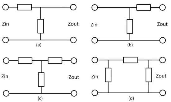
Figure 4.
Different types of impedance matching networks with distributed elements: (a) L-network, (b) Reversed L-network, (c) T-network, (d) π-network [1].
According to the Equation (1), the Q factor defines the bandwidth of the matching network, which is a key parameter when we design an impedance matching network. If a wideband matching network is required, an L-type IMN would be sufficient. But if we have to limit the bandwidth, it is not to be possible to achieve a high Q matching network with L-type network architecture. In that case, we want a network with three elements that provides an additional freedom degree. Thus, with a network with three elements, the designers can choose any value of the Q factor that is higher than that can be possibly achieved by an L-type network. There are two possible configurations, the π-type network and the T-type network [27].
A common application of the π-network is matching a high antenna impedance to the low rectifier impedance. The T-network got its name because the elements form a T-shape as shown in Figure 4c. The T-network is the dual of the π-network. The T-network can be considered as a series combination of two back-to-front L networks.
The performance of the system depends on different features such as the quality of components, frequency, cost, the size, hence we could not select one of these topologies for every application. The networks that are looking to maximize the absorption from the antenna and the output voltage gain have to be designed taking into account the tradeoffs created by the components in the specific circuit [3]. The L matching is frequently used and has only two components, which makes the design and control process match more simple. On the other hand, for example, if a band-pass HF filter needs to be designed, it is better to choose a T or π impedance matching network that achieves wider bandwidth than the L network.
In more detail, if we want to design efficient filters, it is important to understand which type of IMN is better for each application. The LPF (Low Pass Filter) configuration appears a low or high impedance at the harmonic frequencies in order to suppress them. If the LPF presents a high-impedance, then it reflects the harmonics to the source, while if it presents a low-impedance, then it diverts the harmonic energy to the ground plane. In high-impedance LPF commonly a T-type network configuration is used, where the starting element is a series inductor. On the other hand, a low-impedance LPF uses a π-type network configuration, the starting element is a parallel Capacitor. Thus, the most suitable IMN type is determined by the load impedance and/or the source impedance at the harmonic frequency. As it is recommended in [26] commonly we use a T-type network to match low-value impedances (<50 Ω) and an π-type network to match high-value impedances (>50 Ω) [26].
Depending on the circuit requirements, we can create several configurations of impedance matching networks as a combination of the simple types (L, π, Τ), either with lumped elements, such as capacitors and inductors (Figure 5) or with distributed elements, such as stubs and microstrip lines (Figure 4). Distributed elements are preferred at microwave frequencies (3–300 GHz), while lumped elements are generally used at lower frequencies (below 3 GHz). The lumped elements parasitic reactance is avoided in the design and they are operated below the self-resonance frequency [7,28].
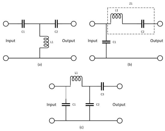
Figure 5.
Different types of impedance matching networks with lumped elements: (a) T-Network (b) L-Network (c) π-Network.
For instance, in [29,30] a self-startup RF power scavenging system with storage capability was designed an impedance matching network with lumped elements (LC). The authors in [31] presented two rectifiers, one half-wave rectifier and one voltage doubler rectifier with the maximum efficiency of the voltage doubler up to 70%. To achieve this, they use an L-matching network. In [32] though, a triple-band rectifier with open stubs operates at 1800, 2100, and 2600 MHz with conversion efficiency to reach 35% at an input power of −20 dBm. The authors in [33] designed an N-stage rectifier. The key research area of this work is the impedance matching network that was used. In addition to the L matching network used, a microstrip line network was designed. The L-network in combination with the microstrip line network is equivalent to the T-network. Figure 6 illustrates an example of the previously mentioned design.
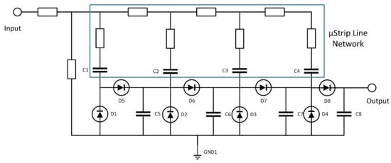
Figure 6.
L-network in combination with the microstrip line network is equivalent to the T- Impedance Matching Network (IMN).
In [34], a triple band differential rectenna was designed with a maximum efficiency of 56% at 3.5 GHz. The impedance matching network of the differential rectenna was consisted of a combination of radial stubs, open stubs, and meander line stubs. The same approach to the impedance matching network with the previous circuit is applied in the dual-band rectifier in [35]. Table 2 lists the aforementioned works of this section.
Table 2.
Different types of Impedance Matching Networks.
3.2.3. Diodes
In rectifier design, one important step is the selection of a diode. The characteristics of the diode determine the overall efficiency of the circuit as it can be the main source for losses because depending on their values, changes the voltage drop across the diode [36]. Conventionally, a Schottky diode was selected because of its low junction capacitance, low threshold voltage, low barrier (high saturation current), and high switching capacity [37]. Low threshold voltage allows more efficient operation at frequencies in which we operate. The junction capacitance will determine the maximum operating frequency at which the diode will operate. These characteristics (Cj is the junction capacitance, Rs is the series resistance, Rj is the junction resistance) are presented in Figure 7a. Figure 7b illustrates the I-V characteristic of a Schottky diode and Figure 7c depicts the symbol of Schottky diode [38].
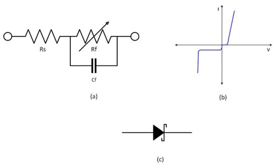
Figure 7.
The characteristics of a diode (a) electronic equivalent circuit (b) I-V characteristic of Schottky diode (c) symbol of Schottky diode.
Table 3 presents the Schottky diodes and their parameters, which are used in several papers in the literature. There are some issues that we need to consider for the proper diode selection. For example, the diode has a nonlinear behavior [39], hence the RF to DC conversion efficiency varies with different power levels of the input. The main goal of the designers is to maximize the harvested RF power; hence they have to minimize the forward voltage drop of the diode and maximize the input voltage level of the rectifier. If the input voltage level of the rectifier is not larger than the forward voltage drop of the diode, then the rectifier circuit doesn’t work. In addition to that, the diode doesn’t work if the reverse breakdown voltage is exceeded [40].
Table 3.
Schottky diodes.
The most commonly used Schottky diodes are the HSMS-285X (n-type) and the HSMS-286X (p-type). The first one has a high fence and low values of Rs, whereas the second one has a low barrier and high values of Rs [7]. In [41] a dual-stage voltage doubler was manufactured for operation at a frequency of 3.5 GHz using HSMS-2820 diodes. In [42] the authors designed three rectifiers and connected them in series. Each rectifier is a single series diode rectifier. For this design, they used an SMS7630-079 diode. A voltage doubler was manufactured in [43] with an efficiency of 50.7% at 2.45 GHz and 20.1% at 5.85 GHz. The authors used the SMS-7630 diode [44].
According to the above, the diode greatly affects the efficiency of the rectifier. The energy conversion efficiency increases when we have a decrease of turn-ON threshold voltage or decrease of junction tension Vj and decreases when we have an increase of resistance Rs or decrease of junction capacitance Cj [7].The authors in [45] designed a dual-band (1800 MHz, 2.1 GHz) rectenna in which the rectification was achieved with a single diode rectifier (by the use of an SMS7630 diode). The efficiency of this work is 33% for −7 dBm input power. The authors have used HSMS-285C diodes in [46] to manufacture and compare a 1-stage Dickson rectifier and a 3-stage Dickson rectifier. The circuits tune in 1 GHz and for −7 dBm input power. The first circuit achieved 70.5% efficiency while the second circuit achieved 77% efficiency. The authors in [47] designed a rectenna in which HSMS-286C diodes were used. The circuit resonates at 868 MHz. The maximum efficiency is 44.5% at −10 dBm. Table 4 lists the most common types of diodes that are used in various rectifiers’ designs.
Table 4.
Types of diodes that are utilized in various rectifiers’ designs.
3.2.4. Rectifier
The rectifier is the fundamental circuit of the rectenna, and its role is to convert the AC output voltage of the receiving antenna to DC voltage. It consists of passive elements (capacitors, coils, resistors) and diodes or diode-connected transistors.
As Figure 8 depicts, there are three basic types of rectifier designs: single diode, voltage multiplier, and bridge of diodes. Single diode and bridge rectifiers can provide a DC voltage to the load, but the amplitude of the output signal is lower than the amplitude of the received signal. More specifically, a half-wave rectifier is the simplest rectifier circuit, but it is rarely used because it diminishes half of the input power [40]. The bridge rectifier circuit rectifies both cycles of the AC input. This circuit has 4 diodes operating simultaneously, hence there is a higher drop voltage. On the other side, a voltage multiplier is a rectifier circuit that not only converts the AC input to DC output but boosts it. At RF energy harvesting systems with a demand of high efficiency and high output power, at low input voltages, the full-wave rectifier is the best choice [48]. When the rectified power is insufficient and there is a demand for further increasing voltage, a better approach is the use of stacking single rectifiers into series (Figure 9), making a voltage multiplier [6,44].
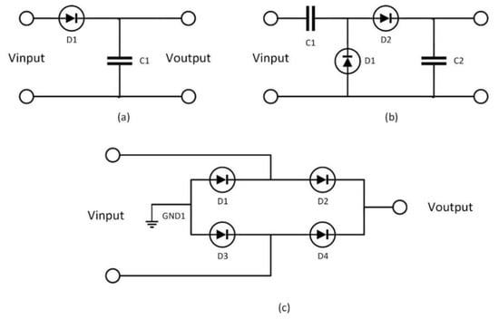
Figure 8.
Types of rectifier configurations (a) half-wave rectifier (b) full-wave rectifier (c) bridge rectifier [1].
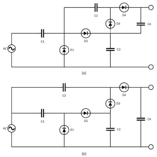
Figure 9.
Topologies of voltage multipliers: (a) Villard Topology (b) Dickson Topology.
In [49] the authors manufactured a rectifier prototype with a single HSMS-2860 Schottky diode at 2.45 GHz. The authors in [50] have designed a rectifier based on the approach of a multiplier. Also, to improve the efficiency of their circuit, they placed a coil at the input of the circuit. As a result, they achieved an efficiency of 81.65% for 0 dBm input at 868 MHz. A different approach of designing a rectifier in a rectenna is presented in [51,52]. In both works, the authors manufactured a modified Greinacher rectifier that receives input from a rat-race coupler, that was used to divide the input RF signal into two signals with equal power and a 180° phase shift. The conventional Greinacher circuit was placed inside the rat-race coupler structure. In the first design, the efficiency enhanced over 5% for input ranges from −20 dBm to −10 dBm. In the second design, the maximum efficiency is 71% for 4.7 dBm input power.
A common practice to improve the efficiency in RF energy harvesting systems is to add a boost converter to the output of the rectifier [53]. In [54], the authors manufactured a low-complexity double diode rectifier that was connected to a commercial boost converter. Implementing this practice, they achieved an efficiency of 21% for input power of −15 dBm at 97.5 MHz. In [55], a design of a compact rectifier for ambient wireless energy harvesting is presented that operates in two frequency bands, namely at 2.4 GHz and 5.8 GHz. The proposed rectifier consists of a dual-band matching network and a voltage quadrupler. It has an efficiency over 70% and can boost up the voltage level up to 9 Volts. In [56] we can find a Latour rectifier. This circuit is practically a modified voltage doubler. The authors achieved 38% efficiency for input −10 dBm at 850 MHz. In [43,57,58,59,60], rectifiers that are voltage doublers can be found. These circuits operate at different frequencies and differ in the choice of materials (capacitors, diodes) and the substrate.
The choice of substrate and diode are two factors that are very important in the design of a rectifier. The authors in [61] designed a Karthaus-Fischer voltage multiplier that which operates at 2.45 GHz. In [62] we can find a 7-stages voltage multiplier that resonances at 900 MHz. A system that works at 575 MHz, 900 MHz, and 2.45 GHz, can be found in [63]. The efficiencies for this system are 55%, 45%, and 30% for each frequency, respectively. In [64] there are four design approaches about differential connection. In [65] there is a 3-stage multiplier that operates at 915 MHz and at 2.4 GHz. The authors in [66] design a rectifier at 2.34 GHz with an input power of −25 dBm. A voltage doubler at 900 MHz can be found in [67] with an efficiency of 78.70% for input power of less than 10 dBm. In [68] a voltage multiplier with multistage Wilkinson was designed. The authors in [69] designed their dual-band rectifier on a polyimide-based substrate, a nonrigid substrate. They achieve at 900 MHz a 20% RF-DC efficiency for −15 dBm input and a 30% for −5 dBm input. At 2.4 GHz they achieve 10% efficiency. The authors of [70] design their rectifier on paper. This is a single diode rectifier because the input power is very low. The authors in [71] designed a single-stage voltage multiplier that operates at 900 MHz. They achieved 50.2% and 49.1% efficiencies for 14 dBm and 16 dBm, respectively. In [72] we can find an RF combiner. This circuit concatenates the RF signals of many rectifiers. Each rectifier is a triple band rectifier (GSM1800, UMTS2100, Wi-Fi). The whole system achieves 40% efficiency. In [73] we can find step by step the process of designing a rectenna on a thin flexible substrate. The whole system can achieve efficiency up to 60%.
The designs of rectifiers with diodes suffer from the high-dropout voltage across the diodes. So, in order to overcome this limitation, the diodes must be replaced with diode-connected MOSFETs (metal-oxide-semiconductor field-effect transistor). Figure 10 below displays a 4-stage Dickson multiplier (Figure 10a) and a conventional differential rectifier (Figure 10b). Over the years and the evolution in circuit design, CMOS technology is preferred, because it assists in custom designing in electronics but also because CMOS transistors, at low voltages, are more sensitive than Schottky diodes [44]. On the other hand, MOS transistors suffer at high RF power due to a reverse current that drains some of the scavenged energy back to the input [74]. For instance, the authors in [37] designed a CMOS Villard multiplier that operates at 400 MHz and 2.4 GHz. The specific circuit achieves a 160% increase in output power over traditional circuits at 0 dBm of input power.
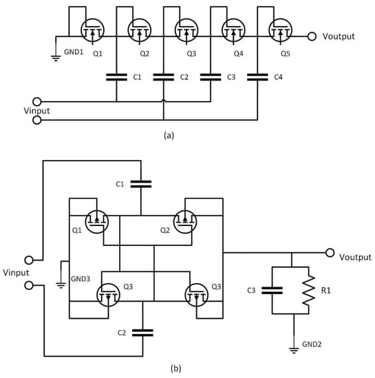
Figure 10.
CMOS rectifier topologies: (a) Dickson Charge Pump (b) Differential Voltage Multiplier.
To overcome some of the limitations such as the low-efficiency and limited working range of the RF energy scavenging systems, many designers manufacture rectennas with reconfigurable rectifiers. For instance, in [29] we can find a self-startup RF power scavenging system with storage capability. The authors in [75] designed a reconfigurable 12-stage rectifier with MPPT (Maximum power point tracking) for input power from −22 to 4 dBm at 915 MHz. A reconfigurable multistage RF rectifier circuit at 900 MHz can be found in [76] with an efficiency of 45% for input power from −15 to 20 dBm. In [77] the authors designed a single-stage receiver in which they used a 3-mode reconfigurable rectifier. The circuit was fabricated in a standard CMOS 0.35 um. This circuit works at 6.78 MHz and achieves 92.2% power efficiency.
Designers constantly try to take advantage of lower input voltages looking for new ways of designing. In a standard CMOS process, a diode is usually replaced more easily with a transistor MOS connected as a diode. The conventional way to implement the MOS-connected (BTMOS) diode with parasitic diodes is shown in Figure 11a, in which the gate is connected to the drain and the bulk to the source. This common connection displays a disadvantage during OFF mode, allowing high reverse current. To overcome the limitation, one solution is to use transistors with a dynamically adjustable threshold voltage, VTH. In the DTMOS (Dynamic Threshold MOSFET) architecture shown in Figure 11b the substrate (bulk) and the gate are connected to dynamically change the VTH of the transistor, using the following equation. In which VTH is the threshold voltage, VT0 is the zero bias threshold voltage with VSB = 0, γ is called body-effect coefficient or body factor and φF is the inversion layer voltage.
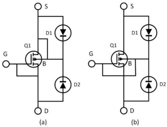
Figure 11.
Diode connected transistors: (a) BTMOS (b) DTMOS.
This not only improves power flow but also minimizes reverse leakage current. Figure 12 shows how the threshold voltage changes to BTMOS and DTMOS for various VSB voltage values [78,79]. The authors in [80] designed a N(1,2,3)-stage rectifier used the DTMOS technique. They achieved for 1-stage at 900 MHz efficiency 79.4% and sensitivity −32 dBm.
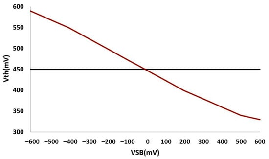
Figure 12.
VT-VSB (The red color refers to DTMOS and the dark blue to BTMOS).
All rectifiers of this section are listed in Table 5. Table 6 consists of the same rectifiers separated by topology.
Table 5.
Different rectifier circuits in bibliography.
Table 6.
List of rectifiers based on their topology.
3.2.5. Load
The most basic parameter that characterizes the quality of RF to DC conversion systems, as shown in the above analysis, is the power conversion efficiency (PCE). PCE refers to the amount of energy transferred from the device and is defined as:
Pin is the RF input power, Pout refers to the output power with Vout as the output voltage and RL as the output load. To achieve maximum efficiency of the device, the load resistance must be adjusted. However, high voltage requires high resistance, according to Ohm’s law. Therefore, trade-off becomes inevitable. From the above equation, we understand the importance of choosing the proper load value. The load can be capacitive, inductive, or purely ohmic. For this reason, all works involved in the design of such circuits are given a special study of what load will be used. As can be deduced from [43,54], the efficiency of the system decreases when the load increases. As a result of the previous analysis, we notice that it is very important that the load impedance be carefully selected for a specific energy harvesting circuit [81]. Figure 13 depicts the change of the PCE depending on the output loads for various power inputs [82].
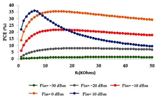
Figure 13.
The change of PCE depends on different output loads.
4. Discussion
Energy harvesting is the process in which energy is harvested from the environment and converted into electrical power. The aim of energy harvesting is the energy autonomy of systems. Energy from the natural resources can be solar, thermal, vibration, friction, or Radio Frequencies (RF) signals and behave differently over time, depending on the operating environment of the system. We focused on RF Energy Harvesting and how an RF EH system, a rectenna, can be designed.
Τhere are two different approaches of energy transfer: the dedicated transfer that means high power values or the harvesting of ambient energy that means low power values.
A rectenna consists of a receiving antenna, an impedance matching network, and a rectifier. The design process includes the selection of the proper energy harvesting circuit topology, the selection of a suitable diode, and the design of an appropriate impedance matching network. At the end of the design process, there is the optimization and simulation of the whole system.
We categorized many designs according to the type of different modules (antennas, impedance matching networks, rectifier circuit) and we mentioned the pros and cons of each topology. Furthermore, we came to some basic conclusions about the design of each unit of the rectenna, which we mention below.
Some antennas are made from several materials and in several designs, such as dipole antennas, Yagi-Uda antennas, microstrip antennas, etc. From the bibliographic research that was performed, no design is used or preferred more than the rest. Maybe in the near future and due to their easy fabrication as well as their small size, microstrip antennas will be preferably selected.
In terms of the design of the impedance matching circuit the most used matching networks, are the L, the reversed L, the π, and the T network. The L matching is frequently used and has only two components, which makes the design and control process match more simple. In some designs it’s better to choose a T or π impedance matching network because these topologies achieve wider bandwidth than the L network. Additionally, the T matching network can be used to improve the output voltage levels. In addition to that, the vast majority of the authors chose to use distributed elements in their designs that are preferred at microwave frequencies (3–300 GHz). The lumped elements are generally used at lower frequencies (below 3 GHz).
The selection of diodes is one of the most critical steps in the design of the rectifier. Usually, Schottky diodes are used because of their low junction capacitance, low threshold voltage, low barrier, and high switching capacity.
A rectifier, which is the fundamental circuit of the rectenna, can be designed with diodes or with MOSFETs. There are benefits to both. But one thing that is clear from all these works is that circuit designers at these frequencies (4G, 5G, etc.) prefer diodes because MOS transistors suffer at high RF power due to a reverse current, which drains some of the scavenged energy back to the input. On the other hand, CMOS technology (BTMOS, DTMOS) sometimes is preferred, because CMOS transistors when operating in low voltages are more sensitive than diodes. Also, as shown in Table 6 above, most designs are voltage doublers and not multipliers because if we use more stages, then we will have a higher drop voltage. In most cases, this is not acceptable.
Many designers design reconfigurable rectifiers to overcome some of the limitations such as the low-efficiency and limited working range of the RF energy scavenging systems. Another practice to improve the efficiency in RF energy harvesting systems is to add a boost converter to the output of the rectifier.
One of the most basic parameters that characterize the quality of a rectenna system is the power conversion efficiency (PCE), which mainly depends on the load, which in turn can be capacitive, inductive, or purely ohmic. In addition to that, in most of the designs studied, the characteristic impedance of the circuits is at 50 Ω and most authors agree on the use of the substrate, with the FR4 substrate being the most common because it is quite cheap.
Energy harvesting is without a doubt a very attractive technique for a large number of self-powered microsystems. Examples of such systems are wireless sensors, implantable medical devices, military surveillance devices, remote weather stations, calculators, watches, Bluetooth, or even mobile phones. There are already companies on the market that have launched mobile phones that charge using RF energy harvesting. With the great development of the Internet of Things (IoT) in recent years, the RF energy harvesting will play a very important role because RF signals are all around us and are inexhaustible. A rectenna system will be very useful in Smart Cities and Smart Homes which is also a huge new scientific field. It aims to solve the power supply problem of the countless sensors used in the IoT to monitor and develop data collection, thus contributing to the need to reduce their battery or power supply.
Finally, we made an extensive analysis of the design of the RF energy harvesting system, but it is not necessary to limit energy scavenging to RF power if other sources are abundantly available. As we mentioned before, other energy sources can be kinetic, chemical, friction, heat radiation, solar, etc. Hence, the future of energy harvesting could be the combination of these types of energy to improve efficiency. This approach is the hybrid systems. Nowadays, for example, hybrid vehicles are the future of the car industry.
5. Conclusions
In this work, we focus on RF Energy Harvesting and wireless power transfer. We have summarized the state-of-the-art RF energy scavenging technology during the last 10 years. A basic RF energy scavenging unit is composed of the following: the antenna, the impedance matching network, and the rectifier. All modules were presented, but we emphasized mostly on the rectifier’s design, which can be designed with diodes or with MOSFETs (BTMOS, DTMOS). Additionally, the power conversion efficiency (PCE) depends on the load of the system and characterizes the quality of a rectenna system. After this literature research, we concluded that most authors use distributed elements to design their impedance matching networks and choose the doubler topology in a rectifier circuit.
Author Contributions
The conceptualization of the paper was done by I.D.B., A.D.B., M.S.P. and S.K.G.; I.D.B. writing—original draft preparation, I.D.B. and K.K. performed the data curation, S.K.G. supervised the process. A.D.B., M.S.P. and K.K. analyzed the methodology and results and contributed to writing the manuscript. All authors contributed to reviewing the manuscript. All authors have read and agreed to the published version of the manuscript.
Funding
This research has been co-financed by the European Union and Greek national funds through the Operational Program Competitiveness, Entrepreneurship and Innovation, under the call RESEARCH-CREATE-INNOVATE (project code: T1EDK-05274).
Institutional Review Board Statement
Not applicable.
Informed Consent Statement
Not applicable.
Data Availability Statement
Data sharing not applicable.
Conflicts of Interest
The authors declare no conflict of interest.
References
- Bougas, I.D.; Papadopoulou, M.S.; Psannis, K.; Sarigiannidis, P.; Goudos, S.K. State-of-the-Art Technologies in RF Energy Harvesting Circuits—A Review. In Proceedings of the 2020 3rd World Symposium on Communication Engineering (WSCE), Thessaloniki, Greece, 9–11 October 2020; pp. 18–22. [Google Scholar] [CrossRef]
- Marian, V.; Allard, B.; Vollaire, C.; Verdier, J. Strategy for Microwave Energy Harvesting From Ambient Field or a Feeding Source. IEEE Trans. Power Electron. 2012, 27, 4481–4491. [Google Scholar] [CrossRef]
- Soyata, T.; Copeland, L.; Heinzelman, W. RF Energy Harvesting for Embedded Systems: A Survey of Tradeoffs and Methodology. IEEE Circuits Syst. Mag. 2016, 16, 22–57. [Google Scholar] [CrossRef]
- Piñuela, M.; Mitcheson, P.D.; Lucyszyn, S. Ambient RF Energy Harvesting in Urban and Semi-Urban Environments. IEEE Trans. Microw. Theory Tech. 2013, 61, 2715–2726. [Google Scholar] [CrossRef]
- Valenta, C.R.; Durgin, G.D. Harvesting Wireless Power: Survey of Energy-Harvester Conversion Efficiency in Far-Field, Wireless Power Transfer Systems. IEEE Microw. Mag. 2014, 15, 108–120. [Google Scholar] [CrossRef]
- Qasem, S.; Husain, M.; Zakaria, Z.; Zin, M.; Alhegazi, A. Rectenna Designs for RF Energy Harvesting System: A Review. Int. J. Commun. Antenna Propag. (IRECAP) 2016, 6, 82–89. [Google Scholar] [CrossRef]
- Almorabeti, S.; Rifi, M.; Terchoune, H. Rectifier Circuit Designs for RF Energy Harvesting applications. In Proceedings of the Colloque sur les Objets et ystems Connectés, Ecole Supérieure de Technologie de Casablanca (Maroc), Institut Universitaire de Technologie d’Aix-Marseille, Aix-en-Provence, France, 17 June 2019. [Google Scholar]
- Congedo, F.; Monti, G.; Tarricone, L.; Cannarile, M. Broadband bowtie antenna for RF energy scavenging applications. In Proceedings of the 5th European Conference on Antennas and Propagation (EUCAP), Rome, Italy, 11–15 April 2011; pp. 335–337. [Google Scholar]
- Boursianis, A.D.; Papadopoulou, M.S.; Nikolaidis, S.; Goudos, S.K. Modified Printed Bow-Tie Antenna for RF Energy Harvesting Applications. In Proceedings of the 2020 IEEE Microwave Theory and Techniques in Wireless Communications (MTTW), Riga, Latvia, 1–2 October 2020; pp. 67–71. [Google Scholar] [CrossRef]
- Khaliq, H.S.; Awais, M.; Ahmad, W.; Khan, W.T. A high gain six band frequency independent dual CP planar log periodic antenna for ambient RF energy harvesting. In Proceedings of the 2017 Progress in Electromagnetics Research Symposium-Fall (PIERS-FALL), Singapore, 19–22 November 2017; pp. 3024–3028. [Google Scholar] [CrossRef]
- Khang, S.-T.; Lee, W.-S.; Yu, J.W. Compact folded dipole rectenna with RF-based energy harvesting for IoT smart sensors. Electron. Lett. 2015, 51, 926–928. [Google Scholar] [CrossRef]
- Saghlatoon, H.; Björninen, T.; Sydänheimo, L.; Tentzeris, M.M.; Ukkonen, L. Inkjet-Printed Wideband Planar Monopole Antenna on Cardboard for RF Energy-Harvesting Applications. IEEE Antennas Wirel. Propag. Lett. 2015, 14, 325–328. [Google Scholar] [CrossRef]
- Zeng, M.; Andrenko, A.S.; Liu, X.; Li, Z.; Tan, H. A Compact Fractal Loop Rectenna for RF Energy Harvesting. IEEE Antennas Wirel. Propag. Lett. 2017, 16, 2424–2427. [Google Scholar] [CrossRef]
- Kamoda, H.; Kitazawa, S.; Kukutsu, N.; Kobayashi, K. Loop Antenna Over Artificial Magnetic Conductor Surface and Its Application to Dual-Band RF Energy Harvesting. IEEE Trans. Antennas Propag. 2015, 63, 4408–4417. [Google Scholar] [CrossRef]
- Sun, H.; Guo, Y.; He, M.; Zhong, Z. A Dual-Band Rectenna Using Broadband Yagi Antenna Array for Ambient RF Power Harvesting. IEEE Antennas Wirel. Propag. Lett. 2013, 12, 918–921. [Google Scholar] [CrossRef]
- Soboll, P.; Wienstroer, V.; Kronberger, R. Stacked Yagi-Uda Array for 2.45-GHz Wireless Energy Harvesting. IEEE Microw. Mag. 2015, 16, 67–73. [Google Scholar] [CrossRef]
- Hu, Y.; Sun, S.; Xu, H. Compact Collinear Quasi-Yagi Antenna Array for Wireless Energy Harvesting. IEEE Access 2020, 8, 35308–35317. [Google Scholar] [CrossRef]
- Shen, S.; Zhang, Y.; Chiu, C.; Murch, R. An Ambient RF Energy Harvesting System Where the Number of Antenna Ports is Dependent on Frequency. IEEE Trans. Microw. Theory Tech. 2019, 67, 3821–3832. [Google Scholar] [CrossRef]
- Agrawal, S.; Gupta, R.D.; Parihar, M.S.; Kondekar, P.N. A wideband high gain dielectric resonator antenna for RF energy harvesting application. AEU-Int. J. Electron. Commun. 2017, 78, 24–31. [Google Scholar] [CrossRef]
- Arrawatia, M.; Baghini, M.S.; Kumar, G. Differential Microstrip Antenna for RF Energy Harvesting. IEEE Trans. Antennas Propag. 2015, 63, 1581–1588. [Google Scholar] [CrossRef]
- Shen, S.; Chiu, C.; Murch, R.D. A Dual-Port Triple-Band L-Probe Microstrip Patch Rectenna for Ambient RF Energy Harvesting. IEEE Antennas Wirel. Propag. Lett. 2017, 16, 3071–3074. [Google Scholar] [CrossRef]
- Boursianis, A.D.; Papadopoulou, M.S.; Gotsis, A.; Wan, S.; Sarigiannidis, P.; Nikolaidis, S.; Goudos, S.K. Smart Irrigation System for Precision Agriculture-The AREThOU5A IoT Platform. IEEE Sens. J. 2020, 21, 17539–17547. [Google Scholar] [CrossRef]
- Boursianis, A.D.; Papadopoulou, M.S.; Pierezan, J.; Mariani, V.C.; Coelho, L.S.; Sarigiannidis, P.; Koulouridis, S.; Goudos, S.K. Multiband Patch Antenna Design Using Nature-Inspired Optimization Method. IEEE Open J. Antennas Propag. 2021, 2, 151–162. [Google Scholar] [CrossRef]
- Lu, X.; Wang, P.; Niyato, D.; Kim, D.I.; Han, Z. Wireless Networks With RF Energy Harvesting: A Contemporary Survey. IEEE Commun. Surv. Tutor. 2015, 17, 757–789. [Google Scholar] [CrossRef]
- Hameed, Z.; Moez, K. Design of impedance matching circuits for RF energy harvesting systems. Microelectron. J. 2017, 62, 49–56. [Google Scholar] [CrossRef]
- AN1275: Impedance Matching Network Architectures. Available online: https://www.silabs.com/documents/public/application-notes/an1275-imp-match-for-network-arch.pdf (accessed on 21 October 2021).
- Khan, D.; Basim, M.; Ali, I.; Pu, Y.; Hwang, K.C.; Yang, Y.; Kim, D.I.; Lee, K.Y. A Survey on RF Energy Harvesting System with High Efficiency RF-DC Converters. J. Semicond. Eng. 2020, 1, 13–30. [Google Scholar]
- Hosain, M.K.; Kouzani, A.Z. Design and analysis of efficient rectifiers for wireless power harvesting in DBS devices. In Proceedings of the 2013 IEEE 8th Conference on Industrial Electronics and Applications (ICIEA), Melbourne, VIC, Australia, 19–21 June 2013; pp. 651–655. [Google Scholar] [CrossRef]
- Abouzied, M.A.; Ravichandran, K.; Sánchez-Sinencio, E. A Fully Integrated Reconfigurable Self-Startup RF Energy-Harvesting System With Storage Capability. IEEE J. Solid-State Circuits 2017, 52, 704–719. [Google Scholar] [CrossRef]
- Nimo, A.; Beckedahl, T.; Ostertag, T.; Reindl, L. Analysis of Passive RF-DC Power Rectification and Harvesting Wireless RF Energy for Micro-watt Sensors. AIMS Energy 2015, 3, 184–200. [Google Scholar] [CrossRef]
- Chuc, D.H.; Duong, B.G. Investigation of rectifier circuit configurations for microwave power transmission system operating at S. band. Int. J. Electr. Comput. Eng. 2015, 5, 967–974. [Google Scholar] [CrossRef]
- Tung, N. Multi-band ambient RF energy harvesting rectifier for autonomous Wireless Sensor networks. In Proceedings of the 2016 IEEE Region 10 Conference (TENCON), Singapore, 22–25 November 2016; pp. 3736–3739. [Google Scholar] [CrossRef]
- Fadel, L.; Oyhenart, L.; Bergès, R.; Vigneras, V.; Taris, T. A concurrent 915/2440 MHz RF energy harvester. Int. J. Microw. Wirel. Technol. 2016, 8, 405–413. [Google Scholar] [CrossRef]
- Chandravanshi, S.; Sarma, S.S.; Akhtar, M.J. Design of Triple Band Differential Rectenna for RF Energy Harvesting. IEEE Trans. Antennas Propag. 2018, 66, 2716–2726. [Google Scholar] [CrossRef]
- Ho, D.K.; Ngo, V.D.; Kharrat, I.; Vuong, T.P.; Nguyen, Q.C.; Le, M.T. Dual-band rectenna for ambient rf energy harvesting at GSM 900 MHz and 1800 MHz. Adv. Sci. Technol. Eng. Syst. 2017, 2, 612–616. [Google Scholar] [CrossRef]
- Jose, J.; George, S.; Bosco, L.; Bhandari, J.; Fernandes, F.; Kotrashetti, A. A review of RF energy harvesting systems in India. In Proceedings of the 2015 International Conference on Technologies for Sustainable Development (ICTSD), Mumbai, India, 4–6 February 2015; pp. 1–4. [Google Scholar] [CrossRef]
- Jabbar, H.; Song, Y.S.; Jeong, T.T. RF energy harvesting system and circuits for charging of mobile devices. IEEE Trans. Consum. Electron. 2010, 56, 247–253. [Google Scholar] [CrossRef]
- Assogba, O.; Mbodji, A.K.; Diallo, A.K. Efficiency in RF energy harvesting systems: A comprehensive review. In Proceedings of the 2020 IEEE International Conf on Natural and Engineering Sciences for Sahel’s Sustainable Development—Impact of Big Data Application on Society and Environment (IBASE-BF), Ouagadougou, Burkina Faso, 4–6 February 2020; pp. 1–10. [Google Scholar] [CrossRef]
- Agrawal, S.; Pandey, S.K.; Singh, J.; Parihar, M.S. Realization of efficient RF energy harvesting circuits employing different matching technique. In Proceedings of the Fifteenth International Symposium on Quality Electronic Design, Santa Clara, CA, USA, 3–5 March 2014; pp. 754–761. [Google Scholar] [CrossRef]
- Cansiz, M.; Altinel, D.; Kurt, G.K. Efficiency in RF energy harvesting systems: A comprehensive review. Energy 2019, 174, 292–309. [Google Scholar] [CrossRef]
- Singh, N.; Kanaujia, B.K.; Beg, M.T.; Mainuddin; Kumar, S.; Choi, H.C.; Kim, K.W. Low profile multiband rectenna for efficient energy harvesting at microwave frequencies. Int. J. Electron. 2019, 106, 2057–2071. [Google Scholar] [CrossRef]
- Shen, S.; Chiu, C.; Murch, R.D. Multiport Pixel Rectenna for Ambient RF Energy Harvesting. IEEE Trans. Antennas Propag. 2018, 66, 644–656. [Google Scholar] [CrossRef]
- ur Rehman, M.; Ahmad, W.; Khan, W.T. Highly efficient dual band 2.45/5.85 GHz rectifier for RF energy harvesting applications in ISM band. In Proceedings of the 2017 IEEE Asia Pacific Microwave Conference (APMC), Kuala Lumpar, Malaysia, 13–16 November 2017; pp. 150–153. [Google Scholar] [CrossRef]
- Tran, L.G.; Cha, H.K.; Park, W.T. RF power harvesting: A review on designing methodologies and applications. Micro Nano Syst. Lett. 2017, 5, 14. [Google Scholar] [CrossRef]
- Khemar, A.; Kacha, A.; Takhedmit, H.; Abib, G. Design and experiments of a dual-band rectenna for ambient RF energy harvesting in urban environments. IET Microw. Antennas Propag. 2018, 12, 49–55. [Google Scholar] [CrossRef]
- Kasar, Ö.; Gözel, M.A.; Kahriman, M. Analysis of rectifier stage number and load resistance in an RF energy harvesting circuit. Microw. Opt. Technol. Lett. 2019, 62, 1542–1547. [Google Scholar] [CrossRef]
- Assimonis, S.D.; Daskalakis, S.; Bletsas, A. Sensitive and Efficient RF Harvesting Supply for Batteryless Backscatter Sensor Networks. IEEE Trans. Microw. Theory Tech. 2016, 64, 1327–1338. [Google Scholar] [CrossRef]
- Divakaran, S.K.; Das Krishna, D.; Nasimuddin, N. RF energy harvesting systems: An overview and design issues. Int. J. RF Microw. Comput. Aided Eng. 2019, 29, e21633. [Google Scholar] [CrossRef]
- Zhou, Y.; Froppier, B.; Razban, T. Schottky diode rectifier for power harvesting application. In Proceedings of the 2012 IEEE International Conference on RFID-Technologies and Applications (RFID-TA), Nice, France, 5–7 November 2012; pp. 429–432. [Google Scholar] [CrossRef]
- Chaour, I.; Bdiri, S.; Fakhfakh, A.; Kanoun, O. Modified rectifier circuit for high efficiency and low power RF energy harvester. In Proceedings of the 2016 13th International Multi-Conference on Systems, Signals & Devices (SSD), Leipzig, Germany, 21–24 March 2016; pp. 619–623. [Google Scholar] [CrossRef]
- Zhang, H.; Zhong, Z.; Guo, Y.; Wu, W. Differentially-fed charge pumping rectifier design with an enhanced efficiency for ambient RF energy harvesting. In Proceedings of the 2017 IEEE MTT-S International Microwave Symposium (IMS), Honololu, HI, USA, 4–9 June 2017; pp. 613–616. [Google Scholar] [CrossRef]
- Gozel, M.A.; Kahriman, M.; Kasar, O. Design of an efficiency-enhanced Greinacher rectifier operating in the GSM 1800 band by using rat-race coupler for RF energy harvesting applications. Int. J. RF Microw. Comput. Eng. 2018, 29, 1–8. [Google Scholar] [CrossRef]
- Visser, H.J.; Vullers, R.J.M. RF Energy Harvesting and Transport for Wireless Sensor Network Applications: Principles and Requirements. Proc. IEEE 2013, 101, 1410–1423. [Google Scholar] [CrossRef]
- Daskalakis, S.; Georgiadis, A.; Bletsas, A.; Kalialakis, C. Dual band RF harvesting with low-cost lossy substrate for low-power supply system. In Proceedings of the 2016 10th European Conference on Antennas and Propagation (EuCAP), Davos, Switzerland, 10–15 April 2016; pp. 1–4. [Google Scholar] [CrossRef]
- Yaldi, I.R.H.; Rahim, S.K.A.; Ramli, M.R. Compact rectifier design for RF energy harvesting. In Proceedings of the 2016 IEEE Asia-Pacific Conference on Applied Electromagnetics (APACE), Langkawi, Malaysia, 11–13 December 2016; pp. 258–262. [Google Scholar] [CrossRef]
- Mabrouki, A.; Latrach, M.; Lorrain, V. High efficiency low power rectifier design using zero bias schottky diodes. In Proceedings of the 2014 IEEE Faible Tension Faible Consommation FTFC 2014, Monaco, Monaco, 4–6 May 2014. [Google Scholar] [CrossRef]
- Mansour, M.M.; Kanaya, H. High-Efficient Broadband CPW RF Rectifier for Wireless Energy Harvesting. IEEE Microw. Wirel. Compon. Lett. 2019, 29, 288–290. [Google Scholar] [CrossRef]
- Mansour, M.M.; Kanaya, H. Compact RF rectifier circuit for ambient energy harvesting. In Proceedings of the 2017 IEEE International Symposium on Radio-Frequency Integration Technology (RFIT), Seoul, Korea, 30 August–1 September 2017; pp. 220–222. [Google Scholar] [CrossRef]
- Zhang, J.; Huang, Y.; Cao, P. An Investigation of Wideband Rectennas for Wireless Energy Harvesting. Wirel. Eng. Technol. 2014, 5, 107–116. [Google Scholar] [CrossRef]
- Taris, T.; Vigneras, V.; Fadel, L. A 900MHz RF energy harvesting module. In Proceedings of the 10th IEEE International NEWCAS Conference, Montreal, QC, Canada; 2012; pp. 445–448. [Google Scholar] [CrossRef]
- Rajawat, A.; Suri, K.; Mohta, M. Design of an efficient rectifier circuit based on karthaus-fischer voltage multiplier for energy harvesting. Adv. Intell. Syst. Comput. 2018, 624, 913–922. [Google Scholar] [CrossRef]
- Devi, K.; Din, N.; Chakrabarty, C. Optimization of the Voltage Doubler Stages in an RF-DC Convertor Module for Energy Harvesting. Circuits Syst. 2012, 3, 216–222. [Google Scholar] [CrossRef]
- Uzun, Y. Design of an efficient triple band RF energy harvester. Appl. Comput. Electromagn. Soc. J. 2015, 30, 1286–1293. [Google Scholar]
- Zeng, M.; Andrenko, A.S.; Liu, X.; Zhu, B.; Li, Z.; Tan, H.-Z. Differential topology rectifier design for ambient wireless energy harvesting. In Proceedings of the 2016 IEEE International Conference on RFID Technology and Applications (RFID-TA), Foshan, China, 21–23 September 2016; pp. 97–101. [Google Scholar] [CrossRef]
- Jolly, A.; Peer, M.; Bohara, V.A.; Verma, S. Design and development of dual-band multi-stage RF energy harvesting circuit for low power applications. In Proceedings of the 2017 IEEE International Conference on Advanced Networks and Telecommunications Systems (ANTS), Bhubaneswar, India, 17–20 December 2017; pp. 1–5. [Google Scholar] [CrossRef]
- Wei, M.; Chang, Y.; Wang, D.; Tseng, C.; Negra, R. Balanced RF Rectifier for Energy Recovery With Minimized Input Impedance Variation. IEEE Trans. Microw. Theory Tech. 2017, 65, 1598–1604. [Google Scholar] [CrossRef]
- Rajawat, A.; Singhal, P.K. Design and implementation of a dual-band rectifier antenna for efficient rf energy harvesting in wireless sensor networks. J. Circuits. Syst. Comput. 2019, 28, 1950034. [Google Scholar] [CrossRef]
- Chong, G.C.; Ramiah, H.; Yin, J.; Rajendran, J.; Wong, W.R.; Mak, P.-I.; Martins, R.P. Ambient RF energy harvesting system: A review on integrated circuit design. Analog. Integr. Circ. Sig. Process. 2018, 97, 515–531. [Google Scholar] [CrossRef]
- Berges, R.; Fadel, L.; Oyhenart, L.; Vigneras, V.; Taris, T. Conformable dual-band wireless energy harvester dedicated to the urban environment. Microw. Opt. Technol. Lett. 2020, 62, 3391–3400. [Google Scholar] [CrossRef]
- Palazzi, V.; Kalialakis, C.; Alimenti, F.; Mezzanotte, P.; Roselli, L.; Collado, A.; Georgiadis, A. Design of a ultra-compact low-power rectenna in paper substrate for energy harvesting in the Wi-Fi band. In Proceedings of the 2016 IEEE Wireless Power Transfer Conference (WPTC), Aveiro, Portugal, 5–6 May 2016; pp. 1–4. [Google Scholar] [CrossRef]
- Muhammad, S.; Tiang, J.J.; Wong, S.K.; Iqbal, A.; Alibakhshikenari, M.; Limiti, E. Compact rectifier circuit design for harvesting gsm/900 ambient energy. Electronics 2020, 9, 1614. [Google Scholar] [CrossRef]
- Shen, S.; Zhang, Y.; Chiu, C.; Murch, R. A Triple-Band High-Gain Multibeam Ambient RF Energy Harvesting System Utilizing Hybrid Combining. IEEE Trans. Ind. Electron. 2020, 67, 9215–9226. [Google Scholar] [CrossRef]
- Palazzi, V.; del Prete, M.; Fantuzzi, M. Scavenging for Energy: A Rectenna Design for Wireless Energy Harvesting in UHF Mobile Telephony Bands. IEEE Microw. Mag. 2017, 18, 91–99. [Google Scholar] [CrossRef]
- Almansouri, A.S.; Ouda, M.H.; Salama, K.N. A CMOS RF-to-DC Power Converter With 86% Efficiency and −19.2-dBm Sensitivity. IEEE Trans. Microw. Theory Tech. 2018, 66, 2409–2415. [Google Scholar] [CrossRef]
- Zeng, Z.; Shen, S.; Zhong, X.; Li, X.; Tsui, C.-Y.; Bermak, A.; Murch, R.; Sanchez-Sinencio, E. Design of Sub-Gigahertz Reconfigurable RF Energy Harvester From −22 to 4 dBm With 99.8% Peak MPPT Power Efficiency. IEEE J. Solid-State Circuits 2019, 54, 2601–2613. [Google Scholar] [CrossRef]
- MMansour, M.; Yamamoto, S.; Kanaya, H. Reconfigurable Multistage RF Rectifier Topology for 900 MHz ISM Energy-Harvesting Applications. IEEE Microw. Wirel. Compon. Lett. 2020, 30, 1181–1184. [Google Scholar] [CrossRef]
- Cheng, L.; Ki, W.; Tsui, C. A 6.78-MHz Single-Stage Wireless Power Receiver Using a 3-Mode Reconfigurable Resonant Regulating Rectifier. IEEE J. Solid-State Circuits 2017, 52, 1412–1423. [Google Scholar] [CrossRef]
- Chouhan, S.S.; Halonen, K. The design and implementation of DTMOS biased all PMOS rectifier for RF energy harvesting. In Proceedings of the 2014 IEEE 12th International New Circuits and Systems Conference (NEWCAS), Trois-Rivieres, QC, Canada, 22–25 June 2014; pp. 444–447. [Google Scholar] [CrossRef]
- Chouhan, S.S.; Halonen, K. The DTMOS based UHF RF to DC conversion. In Proceedings of the 2013 IEEE 20th International Conference on Electronics, Circuits, and Systems (ICECS), Abu Dhabi, United Arab Emirates, 8–11 December 2013; pp. 629–632. [Google Scholar] [CrossRef]
- Asli, A.N.F.; Wong, Y.C. −31 dBm sensitivity high efficiency rectifier for energy scavenging. AEU-Int. J. Electron. Commun. 2018, 91, 44–54. [Google Scholar] [CrossRef]
- Nintanavongsa, P.; Muncuk, U.; Lewis, D.R.; Chowdhury, K.R. Design Optimization and Implementation for RF Energy Harvesting Circuits. IEEE J. Emerg. Sel. Top. Circuits Syst. 2012, 2, 24–33. [Google Scholar] [CrossRef]
- Boursianis, A.D.; Papadopoulou, M.S.; Koulouridis, S.; Rocca, P.; Georgiadis, A.; Tentzeris, M.M.; Goudos, S.K. Triple-Band Single-Layer Rectenna for Outdoor RF Energy Harvesting Applications. Sensors 2021, 21, 3460. [Google Scholar] [CrossRef] [PubMed]


Publisher’s Note: MDPI stays neutral with regard to jurisdictional claims in published maps and institutional affiliations. |
© 2021 by the authors. Licensee MDPI, Basel, Switzerland. This article is an open access article distributed under the terms and conditions of the Creative Commons Attribution (CC BY) license (https://creativecommons.org/licenses/by/4.0/).