
In-Situ Characterisation of Charge Transport in Organic Light-Emitting Diode by Impedance Spectroscopy


Abstract
:
1. Introduction
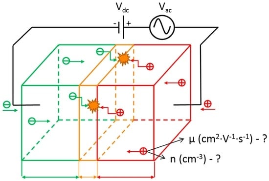
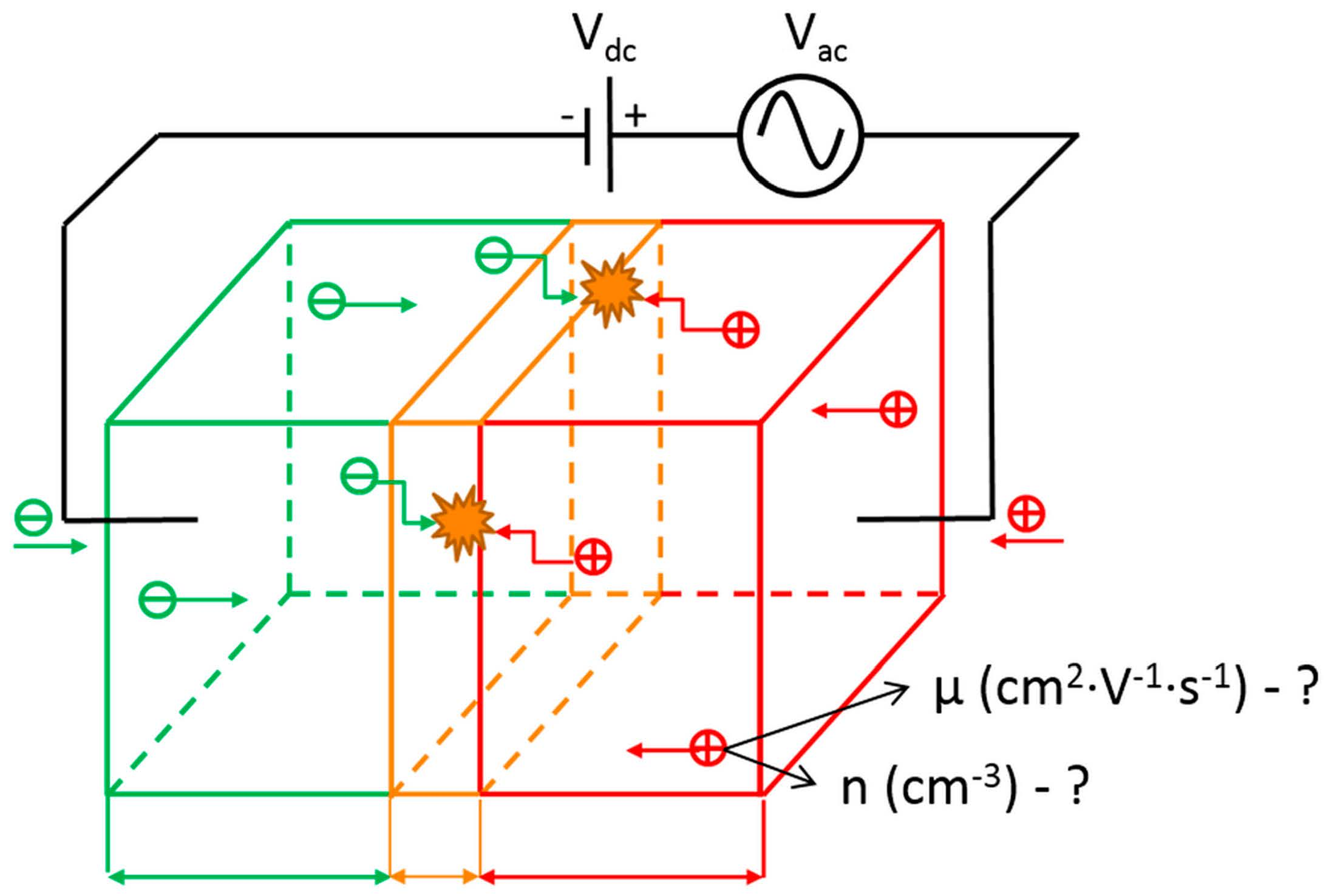
2. Materials and Methods
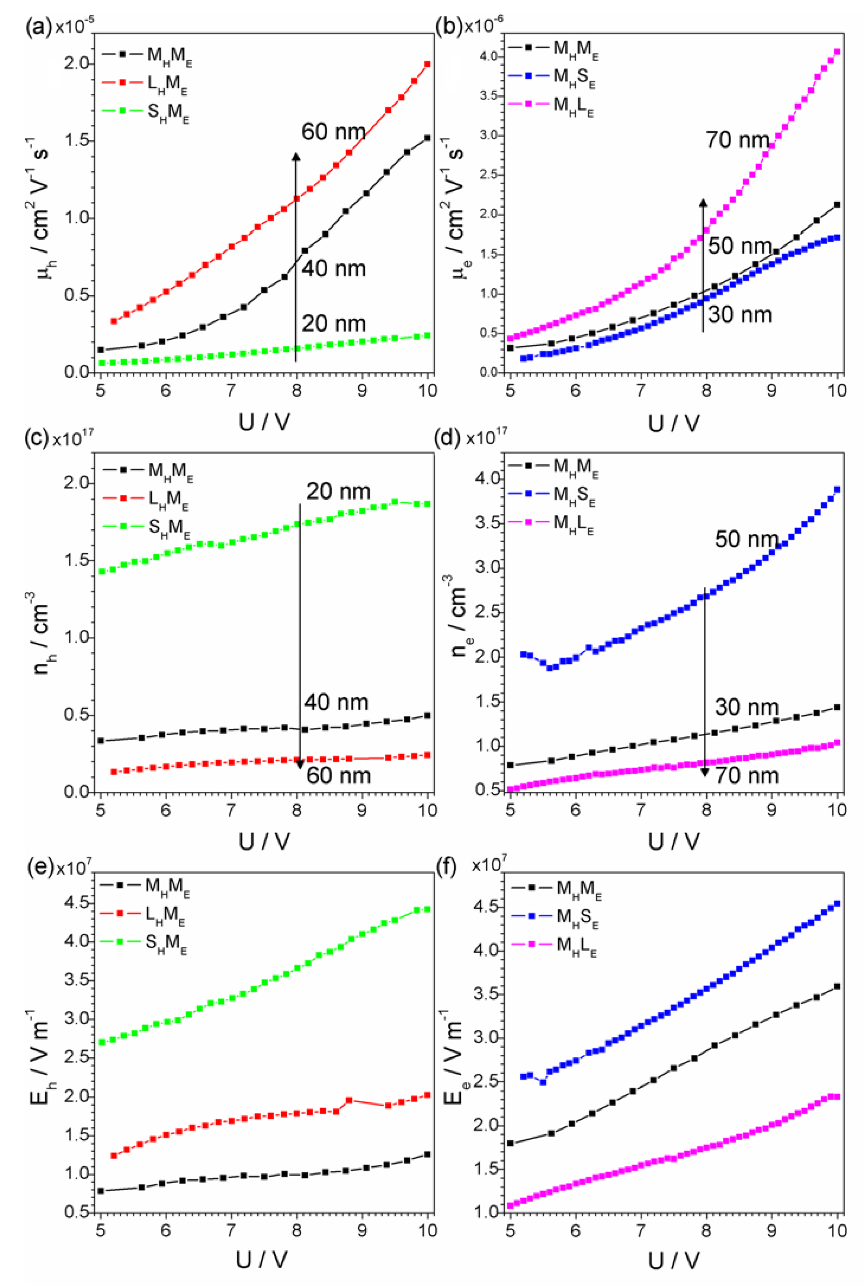
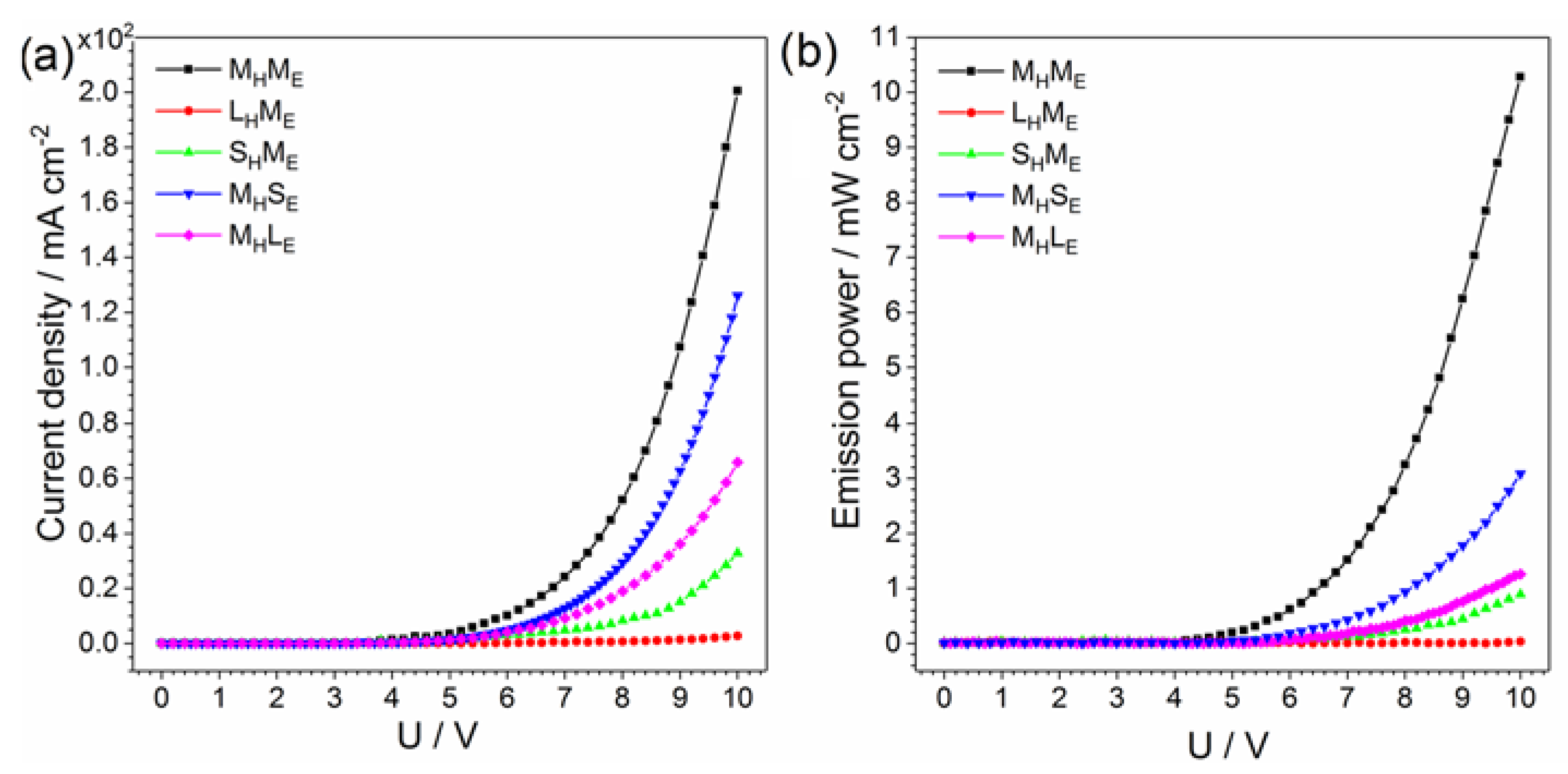
- LHME—ITO|NPB (60 nm)|NPB:TPBi (1:1) (20 nm)|TPBi (50 nm)|LiF (1 nm)|Al
- SHME—ITO|NPB (20 nm)|NPB:TPBi (1:1) (20 nm)|TPBi (50 nm)|LiF (1 nm)|Al
- MHME—ITO|NPB (40 nm)|NPB:TPBi (1:1) (20 nm)|TPBi (50 nm)|LiF (1 nm)|Al
- MHSE—ITO|NPB (40 nm)|NPB:TPBi (1:1) (20 nm)|TPBi (30 nm)|LiF (1 nm)|Al
- MHLE—ITO|NPB (40 nm)|NPB:TPBi (1:1) (20 nm)|TPBi (70 nm)|LiF (1 nm)|Al
3. Results
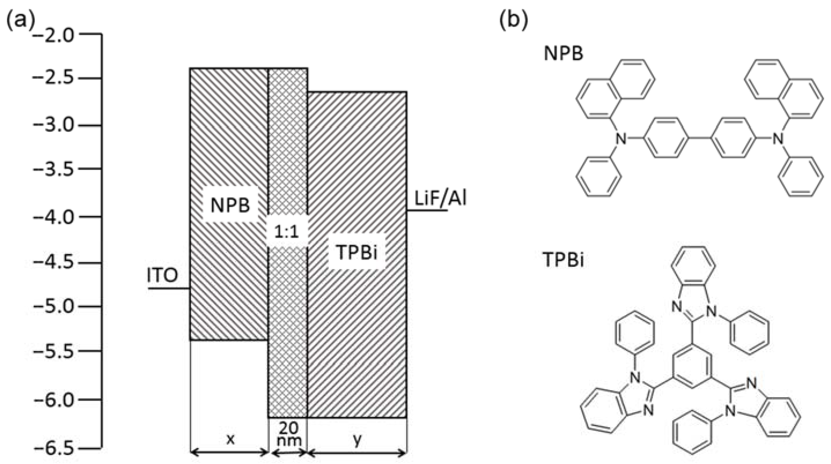
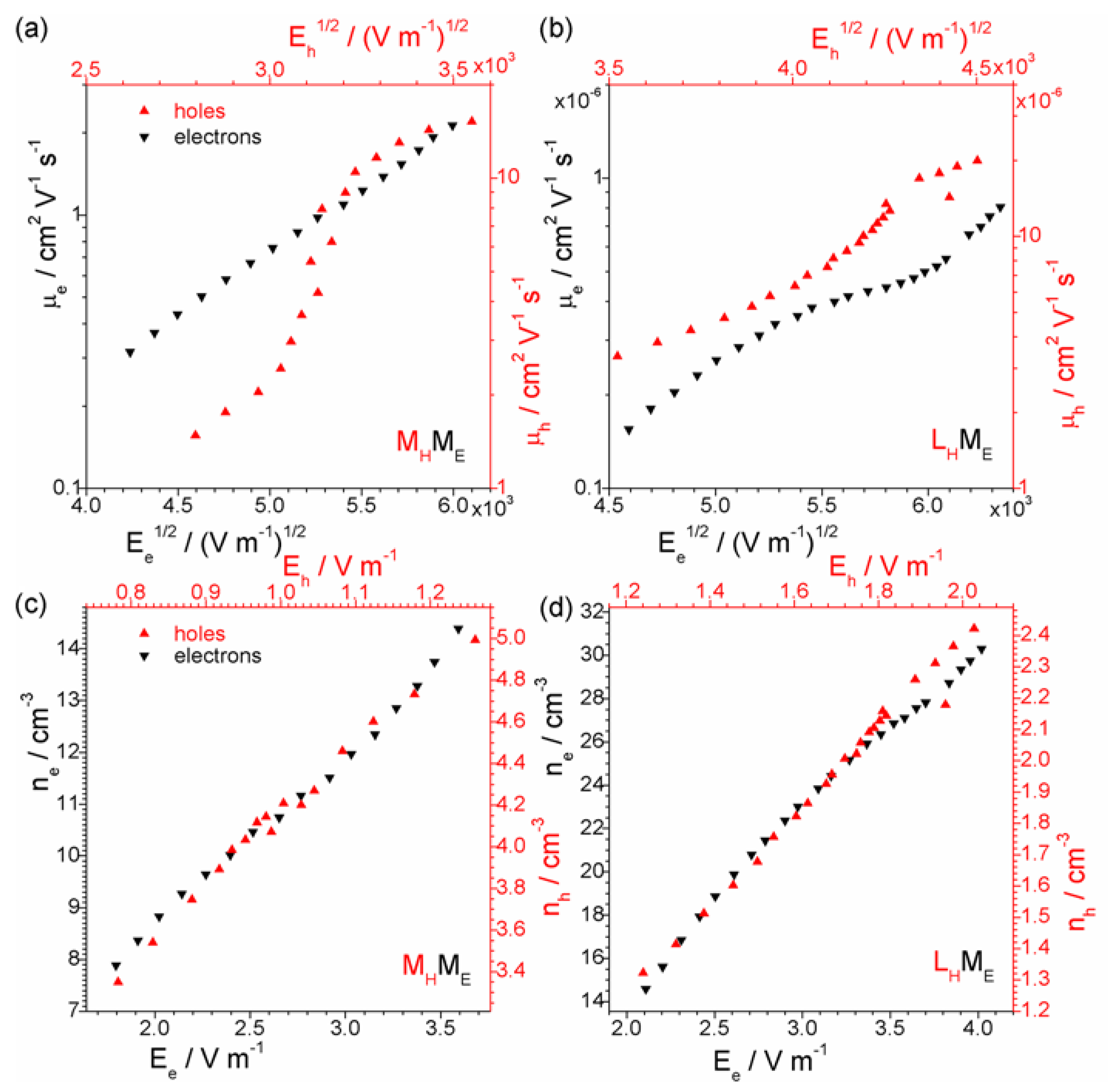
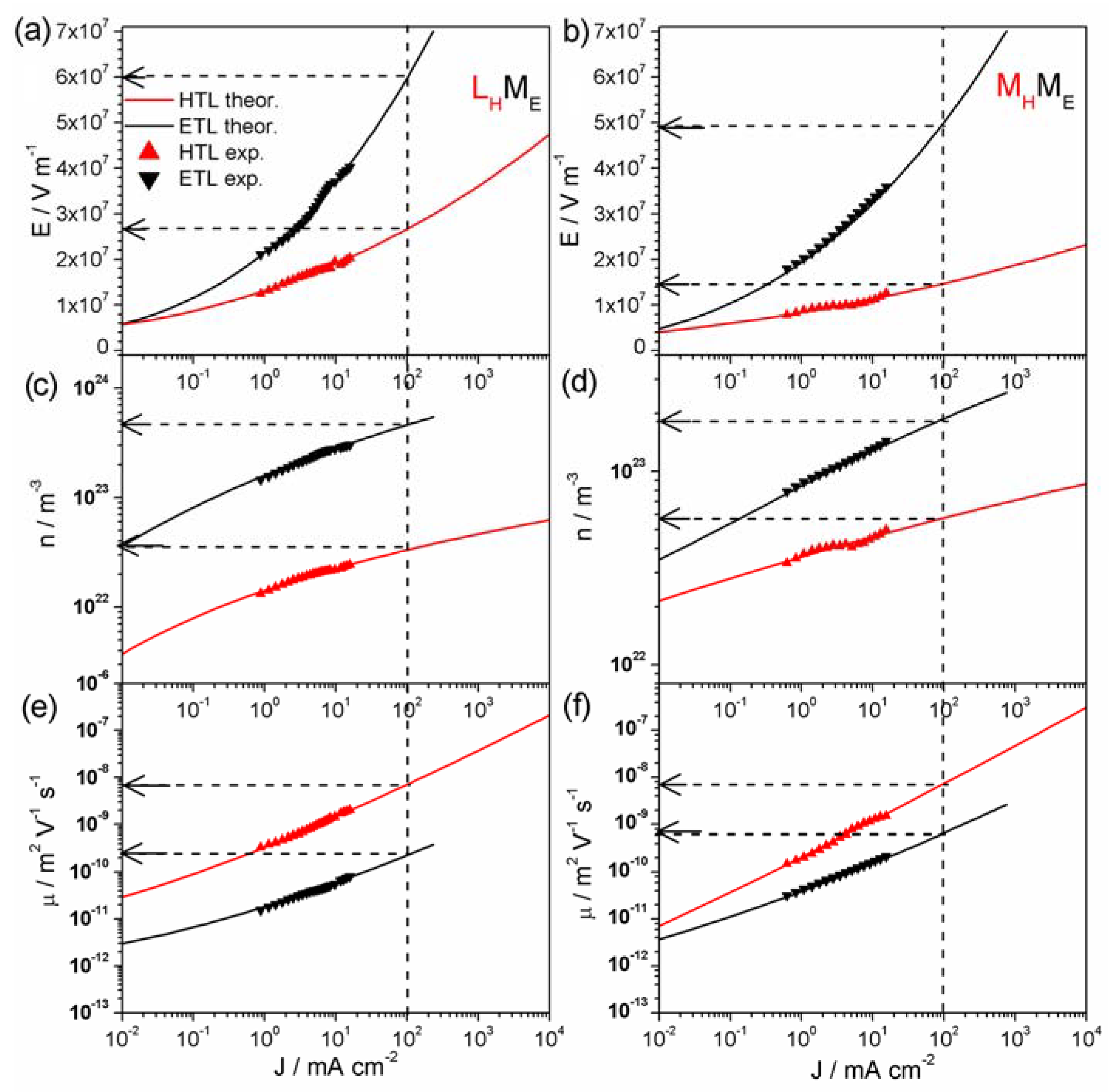
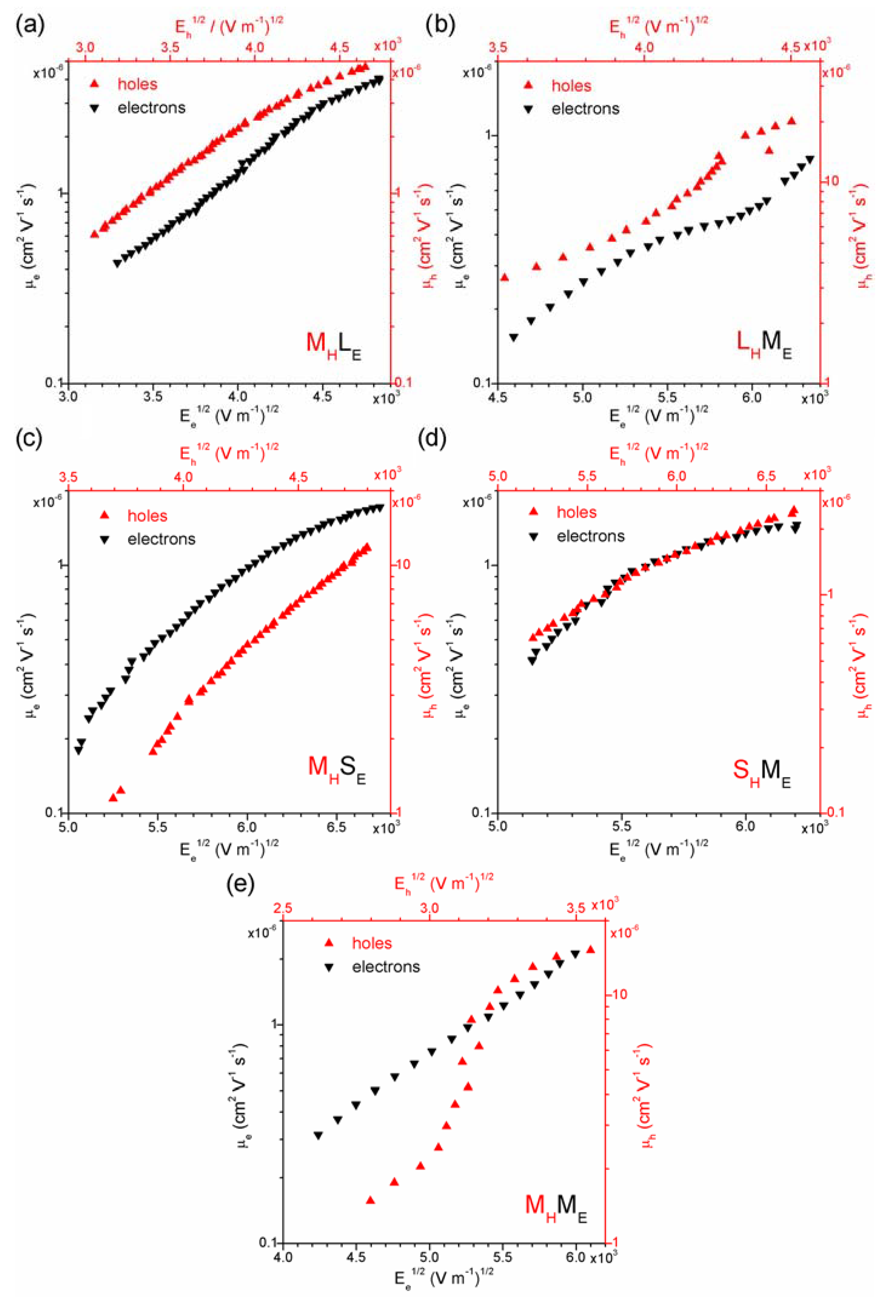
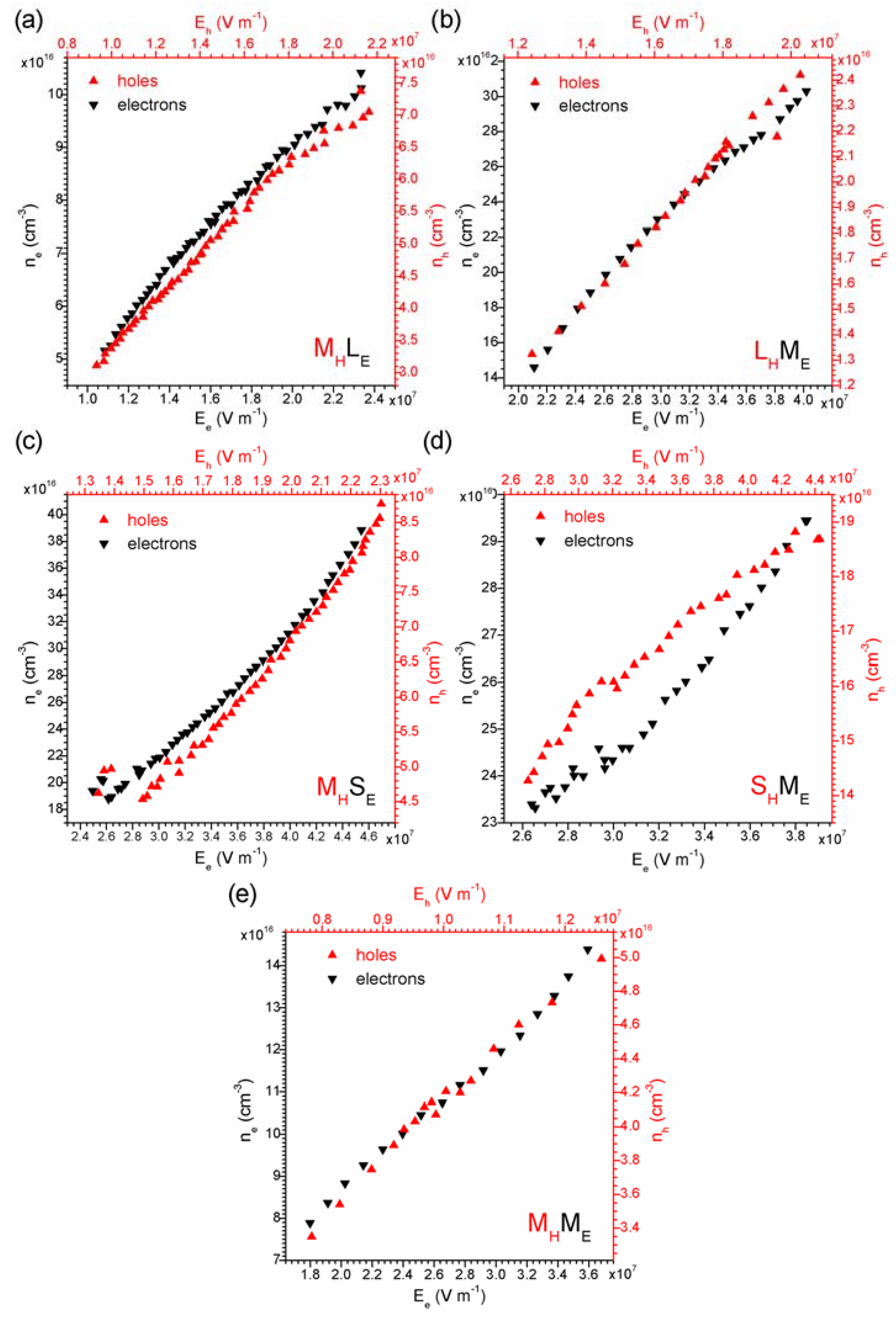
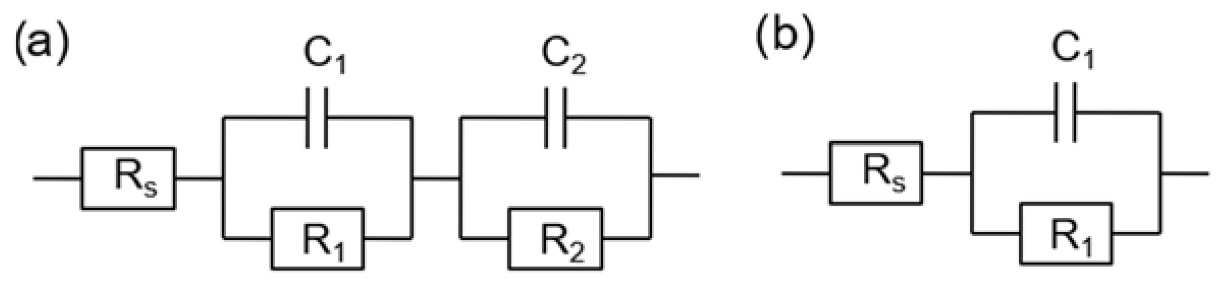
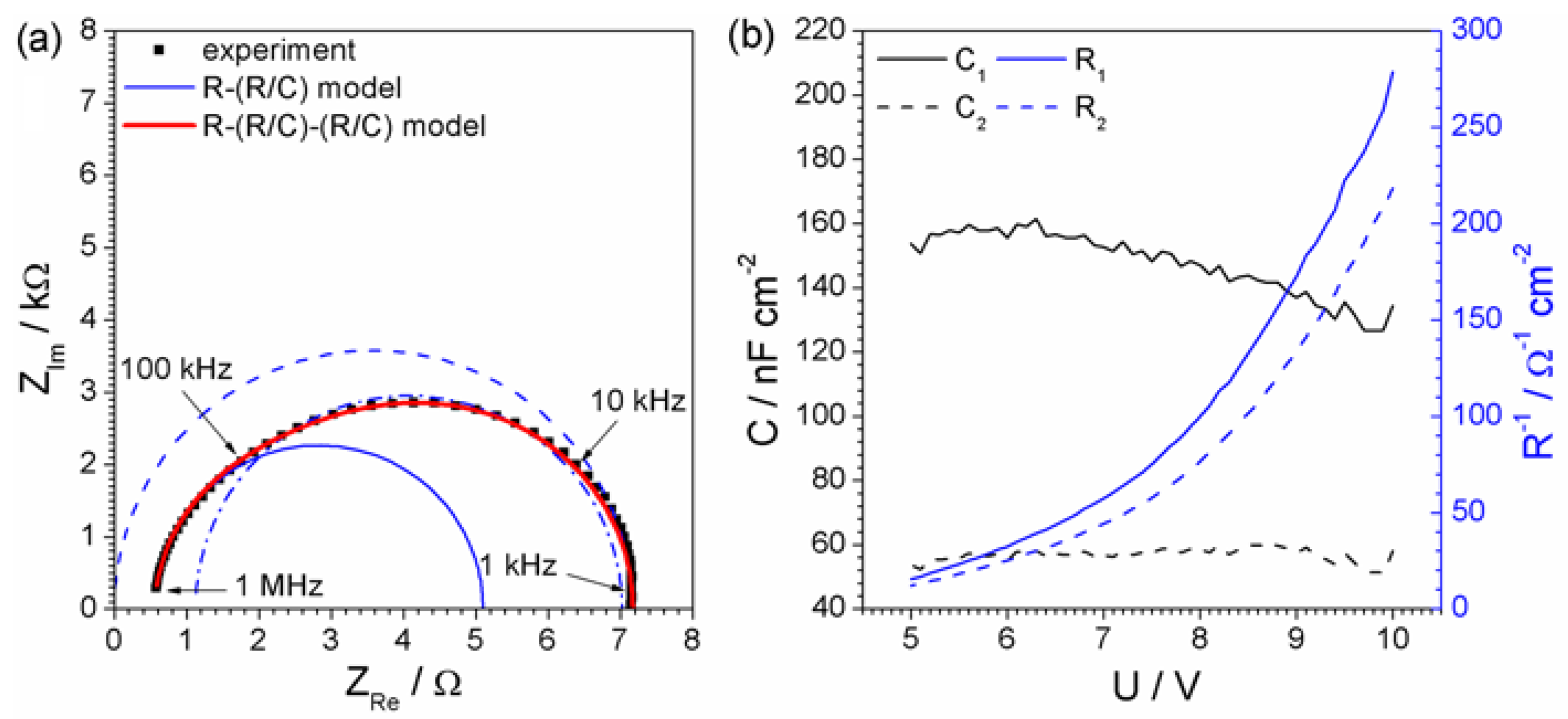
3.1. OLEDs Characterization by Impedance Spectroscopy
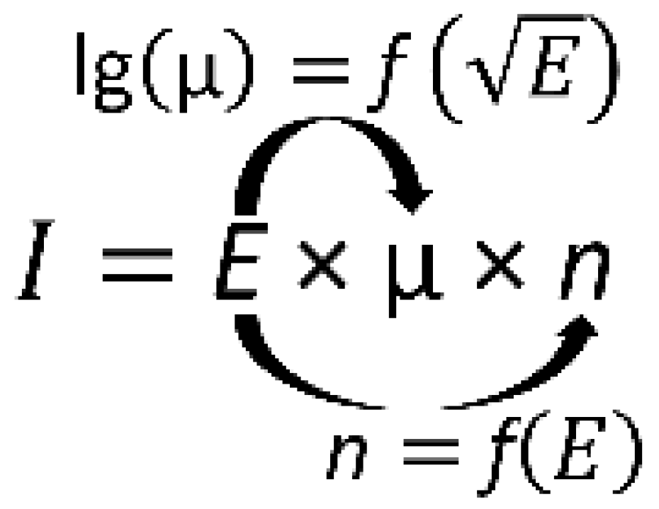
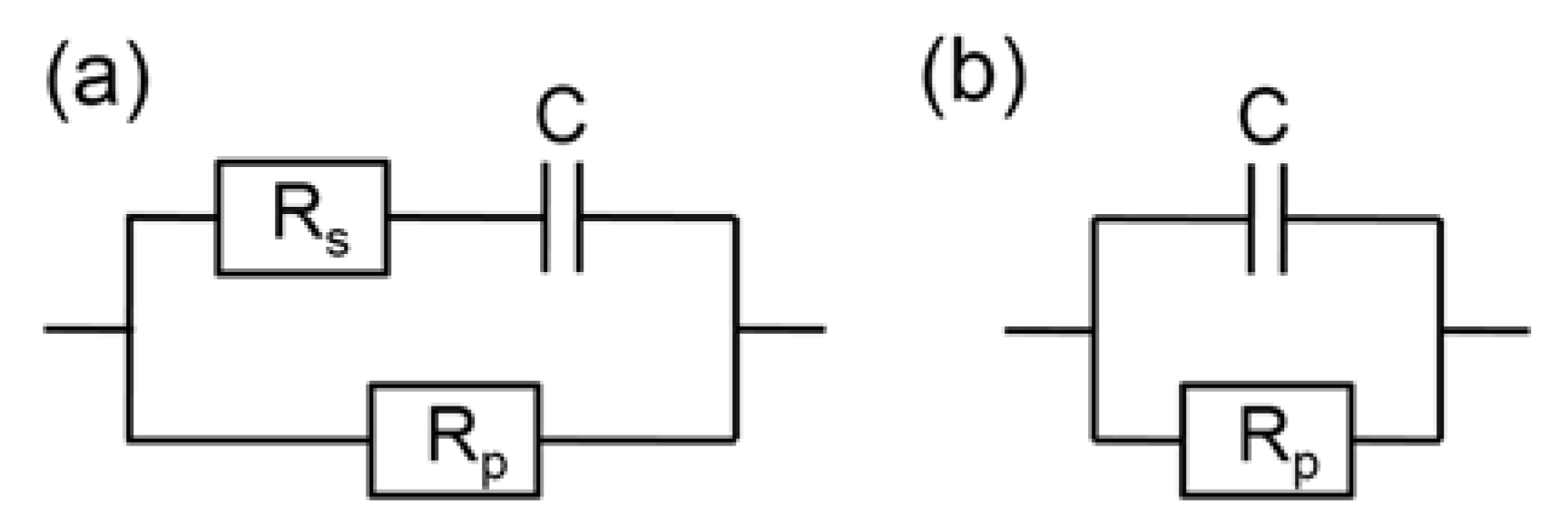
3.2. Experimental Data Processing and Discussion
4. Conclusions
Funding
Institutional Review Board Statement
Informed Consent Statement
Data Availability Statement
Acknowledgments
Conflicts of Interest
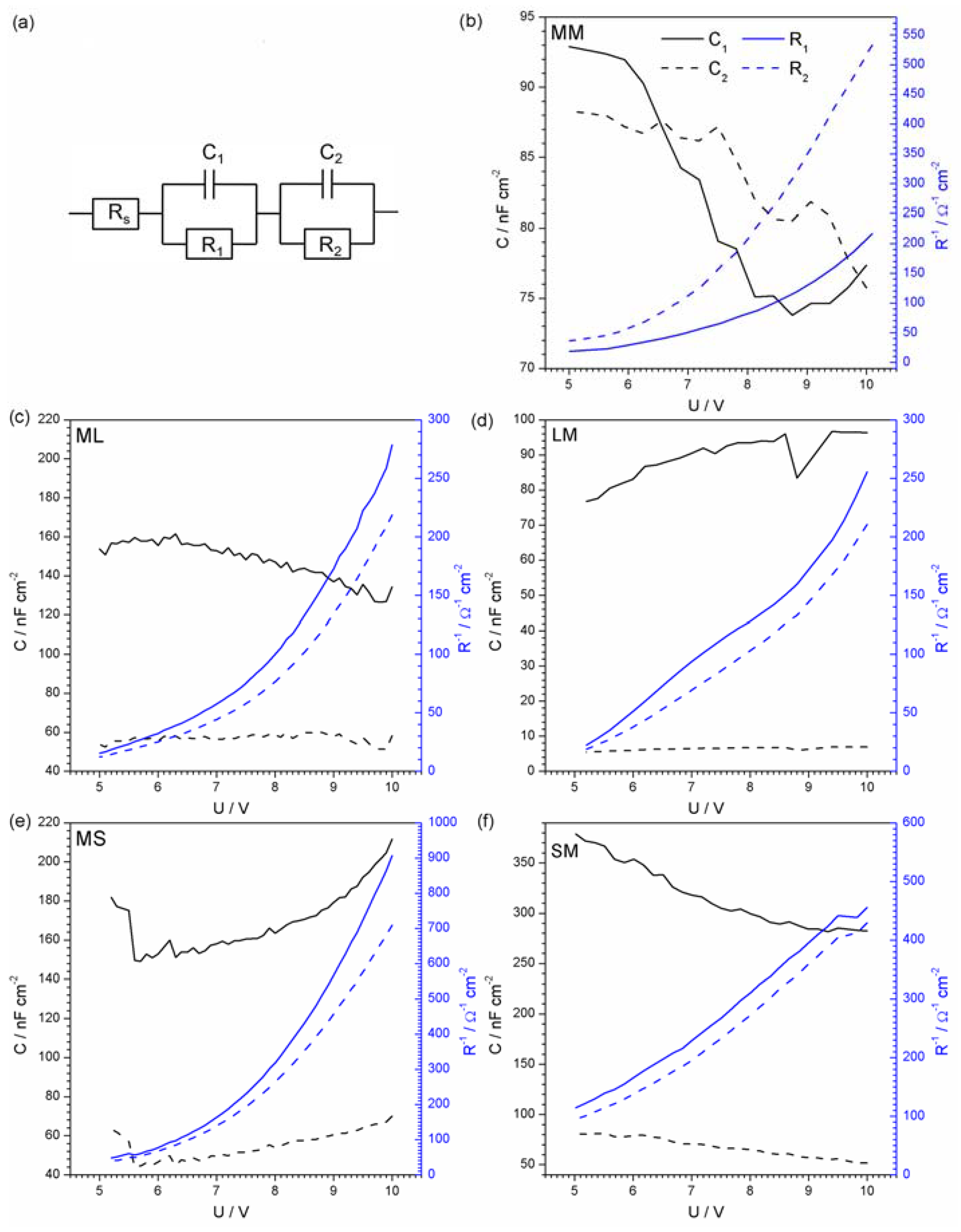
Appendix A. Results on the Characterization of the Diodes: Graphical Data


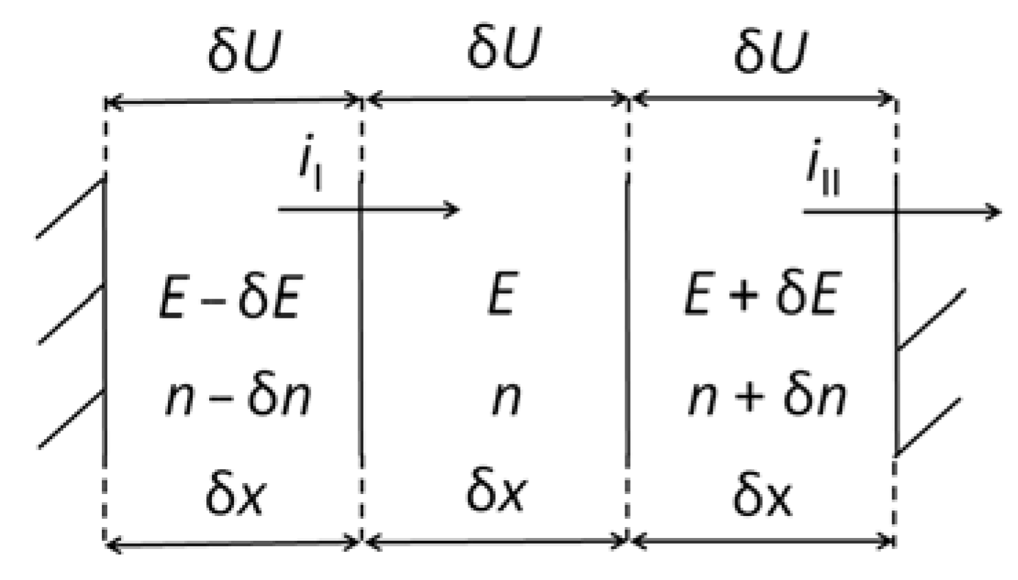
Appendix B. A Detailed Mathematical Procedure for Derivation of the Working Formulas
- F—Faraday constant (96,485 C∙mol−1);
- J—imaginary unit ();
- ε0—vacuum permittivity (8.85∙10−12 F∙m−1);
- ε—relative material permittivity (−);
- R—ideal gas constant (8.314 J∙mol−1∙K−1);
- T—temperature (accepted to be constantly equal to 298 K);
- f—secondary constant, equal to F/RT, introduced for simplification of expressions.
- X—distance (m);
- Δx—thickness of the discrete thin layer (m);
- c—concentration (mol∙m−3);
- δc—a difference of concentration in two neighbour discrete layers (mol m−3);
- D—diffusion coefficient (m2∙s−1);
- J—flux (mol∙m−2∙s−1).
- Electrical parameters:
- i—current density (A∙m−2);
- U—voltage (V);
- δU—voltage drop in a discrete thin layer (V);
- E—electric field intensity (V∙m−1);
- Z, Zre, Zim—impedance (complex value), real and imaginary part (Ω);
- Y—admittance (Ω−1);
- C—capacitance normalized by surface area (F m−2);
- R—resistance normalized by surface area (Ω m2), not to be confused with molar Boltzmann constant, which is always accompanied by T;
- Δi—periodic current density oscillation;
- ΔU—periodic voltage oscillation;
- Δc—periodic concentration oscillation.
- —current phasor;
- —voltage phasor;
- —concentration phasor.

References
- Müllen, K.; Scherf, U. Organic Light Emitting Devices: Synthesis, Properties and Applications; Wiley-VCH: Weinheim, Germany, 2006; ISBN 9783527607235. [Google Scholar]
- Pereira, L. Organic Light Emitting Diodes: The Use of Rare Earth and Transition Metals; CRC Press: Boca Raton, FL, USA, 2012; ISBN 9814267295. [Google Scholar]
- Kitai, A. Luminescent Materials and Applications; John Wiley: New York, NY, USA, 2008; ISBN 9780470058183. [Google Scholar]
- Kalinowski, J.; Cocchi, M.; Virgili, D.; Fattori, V.; Williams, J.A.G. Mixing of Excimer and Exciplex Emission: A New Way to Improve White Light Emitting Organic Electrophosphorescent Diodes. Adv. Mater. 2007, 19, 4000–4005. [Google Scholar] [CrossRef]
- Hung, W.-Y.; Fang, G.-C.; Lin, S.-W.; Cheng, S.-H.; Wong, K.-T.; Kuo, T.-Y.; Chou, P.-T. The First Tandem, All-exciplex-based WOLED. Sci. Rep. 2015, 4, 5161. [Google Scholar] [CrossRef]
- Kim, S.; Kim, B.; Lee, J.; Shin, H.; Park, Y.-I.; Park, J. Design of fluorescent blue light-emitting materials based on analyses of chemical structures and their effects. Mater. Sci. Eng. R Rep. 2016, 99, 1–22. [Google Scholar] [CrossRef]
- Duan, L.; Qiao, J.; Sun, Y.; Qiu, Y.; Duan, L.; Qiao, J.; Sun, Y.D.; Qiu, Y. Strategies to Design Bipolar Small Molecules for OLEDs: Donor-Acceptor Structure and Non-Donor-Acceptor Structure. Adv. Mater. 2011, 23, 1137–1144. [Google Scholar] [CrossRef]
- Li, Y.; Liu, J.-Y.; Zhao, Y.-D.; Cao, Y.-C. Recent advancements of high efficient donor–acceptor type blue small molecule applied for OLEDs. Mater. Today 2017, 20, 258–266. [Google Scholar] [CrossRef]
- Yu, T.; Liu, L.; Xie, Z.; Ma, Y. Chemistry Progress in small-molecule luminescent materials for organic light-emitting diodes. Sci. China 2015, 58, 907–915. [Google Scholar] [CrossRef]
- Gudeika, D.; Lygaitis, R.; Mimaitė, V.; Grazulevicius, J.V.; Jankauskas, V.; Lapkowski, M.; Data, P. Hydrazones containing electron-accepting and electron-donating moieties. Dye. Pigment. 2011, 91, 13–19. [Google Scholar] [CrossRef]
- Coropceanu, V.; Cornil, J.; Da, D.A.; Filho, S.; Olivier, Y.; Silbey, R.; Brédas, J.-L. Charge Transport in Organic Semiconductors. Chem. Rev. 2007, 107, 926–952. [Google Scholar] [CrossRef] [PubMed]
- Cheung, C.H.; Kwok, K.C.; Tse, S.C.; So, S.K. Determination of carrier mobility in phenylamine by time-of-flight, dark-injection, and thin film transistor techniques. J. Appl. Phys. 2008, 103, 093705. [Google Scholar] [CrossRef]
- Chan, C.Y.H.; Tsung, K.K.; Choi, W.H.; So, S.K. Achieving time-of-flight mobilities for amorphous organic semiconductors in a thin film transistor configuration. Org. Electron. Phys. Mater. Appl. 2013, 14, 1351–1358. [Google Scholar] [CrossRef]
- Luo, Y.; Duan, Y.; Chen, P.; Zhao, Y. Effect of hole mobilities through the emissive layer on space charge limited currents of phosphorescent organic light-emitting diodes. Opt. Quantum Electron. 2014, 47, 375–385. [Google Scholar] [CrossRef]
- Chen, C.; Liu, Y.F.; Chen, Z.; Wang, H.R.; Wei, M.Z.; Bao, C.; Zhang, G.; Gao, Y.H.; Liu, C.L.; Jiang, W.L.; et al. High efficiency warm white phosphorescent organic light emitting devices based on blue light emission from a bipolar mixed-host. Org. Electron. Phys. Mater. Appl. 2017, 45, 273–278. [Google Scholar] [CrossRef]
- Tsung, K.K.; So, S.K. Carrier trapping and scattering in amorphous organic hole transporter. Appl. Phys. Lett. 2008, 92, 95. [Google Scholar] [CrossRef]
- Tsung, K.K.; So, S.K. Advantages of admittance spectroscopy over time-of-flight technique for studying dispersive charge transport in an organic semiconductor. J. Appl. Phys. 2009, 106, 083710. [Google Scholar] [CrossRef]
- Okachi, T.; Nagase, T.; Kobayashi, T.; Naito, H. Determination of charge-carrier mobility in organic light-emitting diodes by impedance spectroscopy in presence of localized states. Jpn. J. Appl. Phys. 2008, 47, 8965–8972. [Google Scholar] [CrossRef]
- Ruhstaller, B.; Beierlein, T.; Riel, H.; Karg, S.; Scott, J.C.; Riess, W. Simulating electronic and optical processes in multilayer organic light-emitting devices. IEEE J. Sel. Top. Quantum Electron. 2003, 9, 723–731. [Google Scholar] [CrossRef]
- Ruhstaller, B.; Carter, S.A.; Barth, S.; Riel, H.; Riess, W.; Scott, J.C. Transient and steady-state behavior of space charges in multilayer organic light-emitting diodes. J. Appl. Phys. 2001, 89, 4575–4586. [Google Scholar] [CrossRef]
- Knapp, E.; Ruhstaller, B. Numerical impedance analysis for organic semiconductors with exponential distribution of localized states. Appl. Phys. Lett. 2011, 99, 093304. [Google Scholar] [CrossRef]
- Knapp, E.; Ruhstaller, B. The role of shallow traps in dynamic characterization of organic semiconductor devices. J. Appl. Phys. 2012, 112, 024519. [Google Scholar] [CrossRef] [Green Version]
- Kao, K.C.; Hwang, W. Electrical transport in solids with particular reference to organic semiconductors. Acta Polym. 1982, 33, 663. [Google Scholar] [CrossRef]
- Khan, M.A.; Xu, W.; Zhang, X.W.; Bai, Y.; Jiang, X.Y.; Zhang, Z.L.; Zhu, W.Q. Electron injection and transport mechanism in organic devices based on electron transport materials. J. Phys. D Appl. Phys. 2008, 41, 225105. [Google Scholar] [CrossRef]
- Basham, J.I.; Jackson, T.N.; Gundlach, D.J. Predicting the J—V Curve in Organic Photovoltaics Using Impedance Spectroscopy. Adv. Energy Mater. 2014, 4, 1400499. [Google Scholar] [CrossRef]
- Sacco, A. Electrochemical impedance spectroscopy: Fundamentals and application in dye-sensitized solar cells. Renew. Sustain. Energy Rev. 2017, 79, 814–829. [Google Scholar] [CrossRef]
- Leever, B.J.; Bailey, C.A.; Marks, T.J.; Hersam, M.C.; Durstock, M.F. In Situ Characterization of Lifetime and Morphology in Operating Bulk Heterojunction Organic Photovoltaic Devices by Impedance Spectroscopy. Adv. Energy Mater. 2012, 2, 120–128. [Google Scholar] [CrossRef]
- Chulkin, P.; Vybornyi, O.; Lapkowski, M.; Skabara, P.J.; Data, P. Impedance spectroscopy of OLEDs as a tool for estimating mobility and the concentration of charge carriers in transport layers. J. Mater. Chem. C 2018, 6, 1008–1014. [Google Scholar] [CrossRef]
- Jankus, V.; Data, P.; Graves, D.; McGuinness, C.; Santos, J.; Bryce, M.R.; Dias, F.B.; Monkman, A.P. Highly efficient TADF OLEDs: How the emitter-host interaction controls both the excited state species and electrical properties of the devices to achieve near 100% triplet harvesting and high efficiency. Adv. Funct. Mater. 2014, 24, 6178–6186. [Google Scholar] [CrossRef] [Green Version]
- Pander, P.; Kudelko, A.; Brzeczek, A.; Wroblewska, M.; Walczak, K.; Data, P. Analysis of Exciplex Emitters. Disp. Imaging 2016, 2, 265–277. [Google Scholar]
- Bandarenka, A.S.; Ragoisha, G.A. Inverse Problem in Potentiodynamic Electrochemical Impedance Spectroscopy. In Progress in Chemometrics Research; Nova Science Publishers: New York, NY, USA, 2005; pp. 89–102. [Google Scholar]
- Okachi, T.; Nagase, T.; Kobayashi, T.; Naito, H. Influence of injection barrier on the determination of charge-carrier mobility in organic light-emitting diodes by impedance spectroscopy. Thin Solid Film. 2008, 517, 1331–1334. [Google Scholar] [CrossRef]
- Lasia, A. Electrochemical Impedance Spectroscopy and Its Applications; Springer: New York, NY, USA, 2014; ISBN 978-1-4614-8932-0. [Google Scholar]
- Tsang, S.W.; So, S.K.; Xu, J.B. Application of admittance spectroscopy to evaluate carrier mobility in organic charge transport materials. J. Appl. Phys. 2006, 99, 013706. [Google Scholar] [CrossRef]
- Ruiz, R.; Papadimitratos, A.; Mayer, A.C.; Malliaras, G.G. Thickness dependence of mobility in pentacene thin-film transistors. Adv. Mater. 2005, 17, 1795–1798. [Google Scholar] [CrossRef]
- Gburek, B.; Wagner, V. Influence of the semiconductor thickness on the charge carrier mobility in P3HT organic field-effect transistors in top-gate architecture on flexible substrates. Org. Electron. 2010, 11, 814–819. [Google Scholar] [CrossRef]


Publisher’s Note: MDPI stays neutral with regard to jurisdictional claims in published maps and institutional affiliations. |
© 2021 by the author. Licensee MDPI, Basel, Switzerland. This article is an open access article distributed under the terms and conditions of the Creative Commons Attribution (CC BY) license (https://creativecommons.org/licenses/by/4.0/).
Share and Cite
Chulkin, P. In-Situ Characterisation of Charge Transport in Organic Light-Emitting Diode by Impedance Spectroscopy. Electron. Mater. 2021, 2, 253-273. https://doi.org/10.3390/electronicmat2020018
Chulkin P. In-Situ Characterisation of Charge Transport in Organic Light-Emitting Diode by Impedance Spectroscopy. Electronic Materials. 2021; 2(2):253-273. https://doi.org/10.3390/electronicmat2020018
Chicago/Turabian StyleChulkin, Pavel. 2021. "In-Situ Characterisation of Charge Transport in Organic Light-Emitting Diode by Impedance Spectroscopy" Electronic Materials 2, no. 2: 253-273. https://doi.org/10.3390/electronicmat2020018