Article

Photoelastic Refractive Index Changes in GaAs Investigated by Finite Element Method (FEM) Simulations

by
Daniel T. Cassidy
Department of Engineering Physics, Faculty of Engineering, McMaster University, Hamilton, ON L8S 4L7, Canada
Optics 2025, 6(2), 21; https://doi.org/10.3390/opt6020021
Submission received: 30 January 2025 / Revised: 26 April 2025 / Accepted: 13 May 2025 / Published: 18 May 2025
(This article belongs to the Section Engineering Optics)

Abstract

:
Changes in the refractive indices of a GaAs laser chip owing to bonding strain are investigated by two-dimensional (2D) and three-dimensional (3D) finite element method (FEM) simulations. The strain induced by die attach (i.e., the bonding strain) was estimated by fitting simulations to the measured degree of polarisation (DOP) of photoluminescence from the facet of the bonded chip. Changes in the refractive indices were estimated using the strains obtained from fits to DOP data. Differences between the 2D and 3D FEM estimations of the deformation and of the photo-elastic effect are noted. It is recommended that 2D FEM simulations be used as starting points for 3D FEM simulations. Elastic constants for GaAs in plane-of-the-facet coordinate systems for 2D (plane stress and plane strain) and 3D FEM simulations are given.

1. Introduction

Kirby, Selby, and Westbrook, using analytic expressions for deformation given surface tractions, showed that strain affects the operation of GaAs lasers [1]. Analytic expressions are useful [1,2,3,4,5], but derivation of the expressions usually involves approximations such as semi-infinite media which might compromise the accuracy in real life applications. In addition, not all structures of interest are planar.
Figure 1 shows false colour maps of the measured degree of polarisation (DOP) and rotated degree of polarisation (ROP) of photoluminescence from a cleaved facet through a photonic integrated circuit (PIC). The inset shows schematically, as a cross section, elements that are on the top surface. The top surface is seen edge-on in the figure, and the intersection of the facet with the top-surface is hidden by the magenta coloured areas at the tops of the false colour images. The DOP (and ROP) are sensitive functions of strain [6]. If there was no locally varying strain in the PIC, the DOP and ROP would be uniform and zero. Experimentally it is found that the DOP and ROP are zero for an unprocessed, high-quality wafer.
The constituents of the PIC align with the lobes in the false colour images of the DOP and of the ROP. The question is how to estimate accurately the strain and the changes in refractive index owing to the etching, dielectrics, and metal over-layers shown in the inset. Experience has shown that strain from the over-layers and surface relief affects operation of the PIC.
In this work, 2D and 3D finite element (FEM) simulations of a simple structure are considered. The results from investigations on a simple structure are easier to interpret than for a sample with multiple sources of strain and with surface relief. With a simple structure, the chance of a discrepancy owing to incorrect boundary conditions in the FEM simulation or attribution of an effect to an incorrect source is greatly diminished as compared to a more complex structure.
The goal of this work is to understand if 2D FEM estimates of the deformation and photo-elastic effect, as obtained by fitting 2D FEM simulations to measured DOP data, are accurate representations of the existing deformation. 2D FEM simulations require considerably less computer resources than 3D FEM simulations; 8 s and 0.16 GB of memory versus 280 s and 7.8 GB of memory for the 2D and 3D simulations employed in the work reported in this paper. Fits of simulations to measured DOP data provide a method to make deductions informed by experiment.
The FEM simulations are used to compute the DOP and ROP (collectively DOP) given assumed boundary conditions, and are fit to the measured DOP to obtain estimates of the deformation of the sample. In this manner, the simulations are calibrated by experiment.
The measured DOP (of the photoluminescence) is obtained as
D O P y = P x P z P x + P z
where P x and P z are the measured photoluminescence from a small area (ideally, width of order of a diffraction limited spot ) on the facet and a small depth behind the facet (depth of order of an absorption length in the GaAs) and are polarised in the two orthogonal directions of x and z, and the normal to the measurement surface is in the y direction.
The measured ROP is obtained in a similar manner, except that the measurement axes are obtained by a rotation of the x, y, z Cartesian system about the y axis by 45 deg to create an ( x , y , z ) measurement system [6]. The PL yield equals P x + P z = P x + P z and is the total PL measured for the small area and depth.
The definitions for the measured DOP and ROP, D O P y and R O P y , are general and are independent of alignment of the measurements axes x and z, or x and z , with the GaAs crystal coordinate system that aligns with the unit cell directions of [ 100 ] , [ 010 ] , and [ 001 ] .
The measured DOP and ROP are sensitive functions of strain in III-V materials such as GaAs and InP and the quaternaries of the binary compounds, and the functions of strain depend on the alignment of the measurement axes x and z, and x and z , with the crystal axes [7]. This stands in contrast to the measured DOP and ROP, as described above.
Since the measured surface is a cleaved facet and the goal is to use DOP and ROP measurements to calibrate simulations of deformations, and to use these simulations of the deformations to predict photoelastic changes to the refractive indices, it is necessary to specify the alignment of the measurement coordinate system with the crystal coordinate system.
For the measurements and calculations presented here, the sample is aligned such that the facet is a y = 0 or { 011 } plane with facet normal along the y or 011 direction, the vertical direction is in the z or 100 direction, and the horizontal direction is in the x or 0 1 ¯ 1 direction and is in the plane of the facet. This ( x , y , z ) coordinate system is the usual measurement (coordinate) system.
Figure 2 is composed of schematic diagrams of the sample, and the orientations of the measurement coordinate systems and crystal coordinate systems. Note that the aspect ratio of the sample is not correct in Figure 2. The purpose of Figure 2 is to provide a visual representation of the information on coordinate systems that is presented in the previous paragraph. For the front view, which is a view of the measurement surface, D O P y measurement axes, ( x , y , z ) , are shown in black whereas R O P y measurements axes, ( x , y , z ) , are shown in red.
The cleavage planes for III-V materials such as GaAs, InP, (crystals of InP and GaAs have a cubic structure with an F 4 ¯ 3 m space group symmetry) and related quaternaries are { 011 } planes [8] (Section 2.2). It is thus necessary to rotate all tensors that are determined in the crystal coordinate system by 45 deg about the z axis to obtain values to use in calculations in the plane of the facet. This coordinate rotation should not be confused with the rotation of 45 deg about the surface normal to obtain the ( x , y , z ) coordinate system used to measure the ROP.
The simulated DOP and ROP are obtained from the expressions
D O P 011 = K e 1.252 e x x 0.8132 e z z R O P 011 = K e 1.4083 × 2 e x z ,
which are valid for a cleaved facet of GaAs and the usual measurement (coordinate) system [7]. In this expression, K e = | 3 b / 4 k B T | is a calibration constant and equals 58 0.6 at temperature T = 296 ± 3 K , K B is Boltzmann’s constant, and b is a shear deformation potential; e x x and e z z are the strains along the x and z directions; and, e x z is the tensor shear strain. The calibration constant has been estimated through measurement to be K e = 50 ± 10 for GaAs [9,10]. The subscript 110, which is an equivalent normal to a cleaved facet, has been added to reinforce the idea that the expressions are valid for a facet and for the usual orientation of the coordinate system. As it is cumbersome to typeset, the subscript will be dropped when there is little chance of confusion. The expressions for D O P 011 and R O P 011 are based on analytic expressions for the strain dependence of the band structure of III-V materials [11,12] and the GaAs band parameters from Vurg et al. [13].
The strains or equivalently the stresses in a sample can be estimated from a minimum mean squared error (mmse) fit of the simulated DOP and ROP to the measured DOP and ROP. The fits provide a calibration for calculation of the deformation in the sample. From the calculated deformation, the changes in the refractive index of the GaAs can be obtained as
Δ n x = n o 3 2 × 0.2245 e x x + 0.0805 e y y + 0.1400 e z z Δ n z = n o 3 2 × 0.1400 e x x + 0.1400 e y y + 0.1650 e z z
where e x x , e y y , and e z z are the strains in the plane of the facet, n o = 3.521 is the refractive index when the deformation is zero, n x and n z are the deformation-induced changes in the refractive indices for light that is polarised along the x and z directions and is propagating along the y direction [14] (pp. 241–251), [15] (p. 111), and [16,17,18].
In this work, the effect of shear strain on the refractive index has not been included. Shear causes a rotation of the indicatrix and a rotation of the plane of polarisation as light propagates through the regions of shear [19,20,21]. The non-zero regions of ROP in Figure 1 act as a spatially varying ‘wave plate’, with the sign and magnitude of the rotation varying with the ROP values, which are displayed by a false colour mapping. However, for this work, the propagation length in the shear field is ≲200 nm and neglect of the shear strain in determination of Δ n should not impact the results to any degree. For sufficiently long interaction lengths, the rotation of the plane of polarisation can be appreciable.
For light propagating the length L of a laser, the phase change Δ θ of the electric field of the light is Δ θ = 2 π n L / λ where n is the refractive index and λ is the vacuum wavelength of the light. If the light is propagating in a strain field, then the change in phase owing to the strain is Δ θ ( e ) = 2 π Δ n x L / λ for light that is polarized in the x direction. For a high-power laser, L can be of order 10 mm, λ = O ( 1 μ m ) , strain is typically < 0.001 , which from Equation (3) suggests Δ n < 0.001 also, and Δ θ ( e ) = O ( 3600 deg ) for strain at the upper level of 0.001 . For this laser, propagation through the assumed strain can be similar to propagation through multiple waveplates.
In this work, the light is created by photoluminescence (PL) and the propagation length of the PL is of order of the absorption length of the pump light in the GaAs, which is <200 nm. For the PL and assuming Δ n = 0.001 as for the laser then, Δ θ ( e ) = O ( 0.1 deg ) , which is a negligible fraction of a wave plate, and the shear strain will not introduce a significant rotation of the indicatrix over the absorption length and thus the effects of the shear strain can be ignored.
Estimations of the photo-elastic effect (i.e., changes in the refractive index with deformation) are only as accurate as the underlying FEM simulation used to estimate the deformation of the sample. Thus to ascertain the accuracy of the estimations of the photo-elastic effect, and whether 2D simulations are adequate to the task, it is necessary to ascertain the accuracy of the FEM simulations of the deformation of the sample. To determine the accuracy, results from 2D and 3D FEM simulations and fits of these simulations to measured and synthetic DOP data are compared. 2D FEM approximations, such as plane stress and plane strain approximations, can not fulfil completely boundary conditions on a 3D object.

Organisation of the Paper

The Introduction provided the rationale for the investigation and provided some basic equations and concepts that are key to the investigation. The overarching goal of the investigation was to determine if fits of 2D FEM simulations to measured DOP and ROP were accurate enough to forego computer-resource expensive 3D FEM simulation.
A description of the GaAs laser sample and the results of the investigation are contained in the Section entitled “Sample and FEM Simulations”, Section 2. False colour maps of the measured DOP and ROP of photoluminescence (PL) for the simple sample are presented in this section. Tables that report the quality of fits and fit values are given, and plots of the stresses and changes of refractive indices are contained in this section. To understand the fits, synthetic data were created and plane strain and plane stress simulations, (i.e., 2d FEM simulations) were fit to the synthetic data. Unlike the measured DOP and ROP, the synthetic data had no noise to confuse interpretations.
The Conclusion provides a summary of the results obtained in this manuscript. It is reported that 2D FEM simulations do not provide the accuracy required, particularly within 10 to 20 μ m of boundaries, and thus 2D FEM simulations are probably best used to estimate the boundary conditions for 3D FEM simulations. The 2D FEM simulations require significantly less computer resources than 3D FEM simulations, and that is why 2D FEM simulations are useful to search by trial and error for boundary conditions that provide results that resemble the experimental measurements, and thus provide starting points for 3D FEM simulations.
Appendix A provides summaries of linear elasticity theory and of the GaAs elastic constants used in this work. Appendix B provides information on the photo-elastic effect for GaAs. If desired, Equation (3) could be rewritten as functions of stress, and the equations to achieve the rewriting are given in this appendix.
Appendix C and Appendix D provide developments for the elastic constants required to implement the 2D approximations of plane strain and plane stress. In these appendices it is shown that the plane strain and plain stress elastic constants can be obtained as the c [ y , y ] or s [ y , y ] minors of the 3D stiffness and compliance matrices. The stiffness and compliance matrices are given in the first appendix, Appendix A.

2. Sample and FEM Simulations

The sample is taken to be a GaAs laser chip of thickness 98 μ m, width of 501 μ m, and length of 5 mm, that was soldered to a sub-mount. The bottom metal did not extend to the sides of the chip but stopped 24.5 μ m from the left and right edges of the chip. The top surface of the chip was a free surface, devoid of any metal or dielectric over-layers. The lack of top-surface forces reduced the number of degrees of freedom and thereby made modelling and interpreting the data simpler than for a device with top-surface forces.
Assume an orientation of the GaAs chip and a coordinate system such that z is the vertical or growth direction, y = 0 is the plane of a facet, and the x axis points to the right and along a horizontal direction in the plane of the facet, as described in the Introduction and shown in Figure 2.
Using the PL data to find dimensions [22] (Section 3.1), trial and error, and then grid searches over variables, it was discovered that good agreement with the measured DOP data would be obtained with boundary conditions, on the bottom of the chip, of biaxial strain e = e x x = e y y and a radius of curvature R = R x = R z . The rationale for the biaxial strain on the bottom of the chip was to account for a mismatch in the coefficient of thermal expansion (CTE) between the chip, solder, and sub-mount. The radius of curvature, as a boundary condition independent of the biaxial strain, was used to account for the presence of the sub-mount. By using e and R as independent boundary conditions, it was not necessary to waste resources on gridding the sub-mount and solving for the deformations in the sub-mount.
The values of e and R were determined from a least squares analysis, similar to the least squares fitting procedure described in Ref. [22] (Section 2.1), by minimising the mean square error between the measured DOP and ROP and the FEM simulations of D O P 011 and R O P 011 , Equation (2). It is worthwhile to remark that the boundary conditions and hence the deformation of the GaAs laser chip were determined by fitting to experimental measurements. The results are guided by experiment and not solely by wishes or educated guesses.
In calculations to obtain fits of the simulations to the DOP data, the first 40 columns of data on the left-hand side of the sample were ignored. It was discovered that there is a slight left-right asymmetry to the DOP and ROP data. Fits ignoring the first 40 columns of data on the left-hand side or ignoring the first 40 columns of data on the right-hand side gave similar results, with the quality of fits excluding one side or the other being better than for fits that included both left- and right-hand sides. It was decided arbitrarily to use fits that excluded the first 40 columns of data on the left-hand side.
Figure 3 shows the grid in the plane of the facet upon completion of the best fit 3D FEM simulation, and, with a magnification of 400 × , the deformation of the chip in the horizontal and vertical directions owing to the bonding stress and bottom metal on the GaAs chip. The most notable deformation in the figure is a radius of curvature R (i.e., the smile) imparted to the chip by the boundary conditions that were found to give a best fit of the measured DOP and ROP to the simulated DOP and ROP.
Note that only the right-hand half of the chip was simulated as the boundary on the left-hand side, an x = 0 plane, is a plane of symmetry. The application FlexPDE was used to perform the FEM simulations [23].

Results

Figure 4 shows false colour maps of the data and best fit 3D simulations of D O P 011 and R O P 011 , or just DOP and ROP for brevity, for the facet, which is a y = 0 plane. To map data to a colour, a display gain is chosen and the product of the display gain and the data is converted to the nearest integer, which is used to select a colour to represent a data point. All data points are represented by a rectangle of the same size.
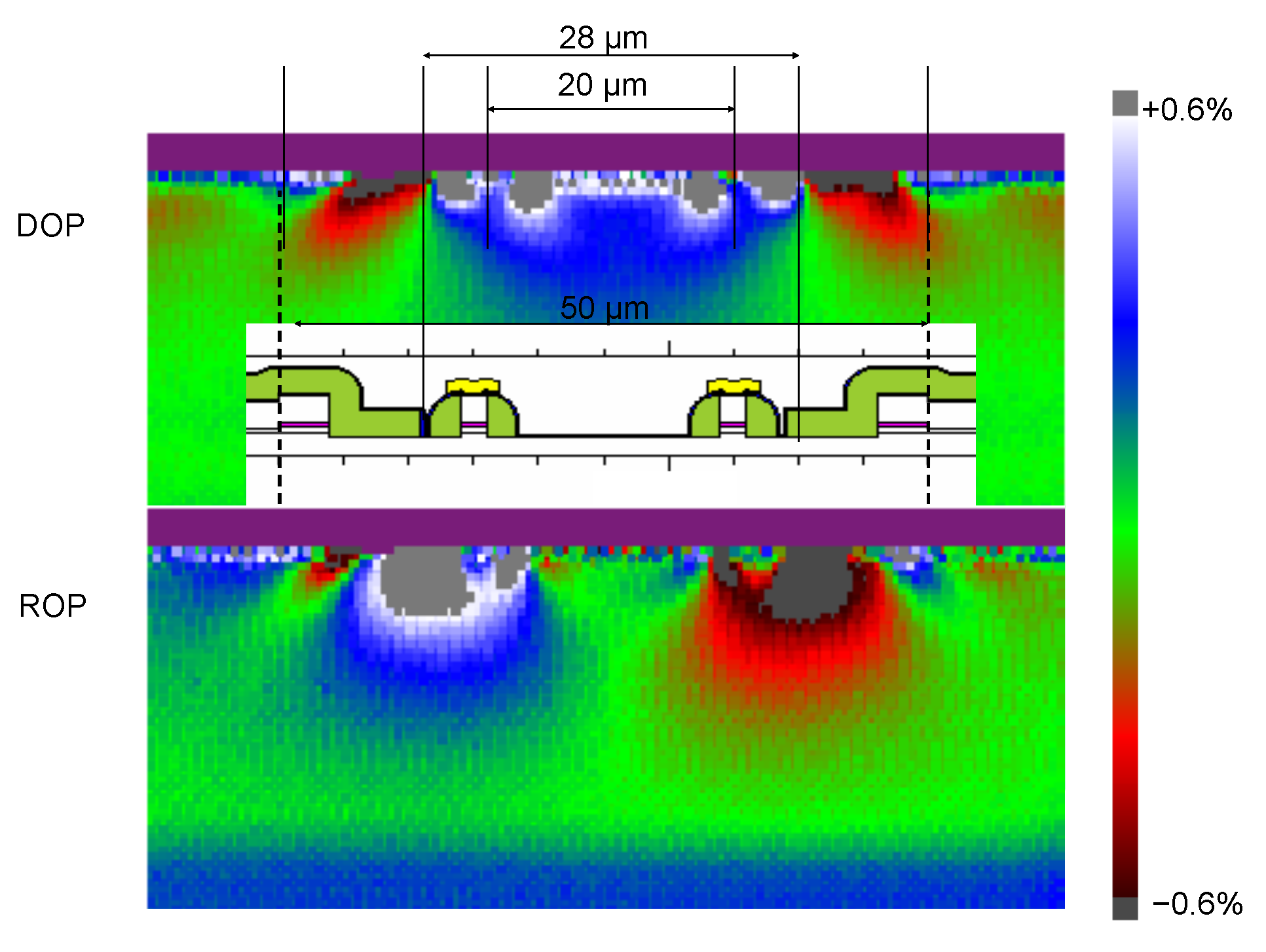
The top row of Figure 4 displays the PL yield for two different values of thresholding. Part (a) shows the PL yield with thresholding of 1 % of the maximum value of the PL. Areas with PL below the threshold level are shown in magenta. This thresholding allows areas of high noise to be suppressed. Part (e) shows the same measured PL yield, but displays the PL yield with a threshold level of 70 % of the maximum value of the PL. This threshold was used to exclude DOP and ROP data from the fits and displays. Any DOP or ROP data that were calculated with a value of the PL yield that was below the threshold value are displayed with a magenta colour. The thresholded data is possibly corrupted by noise or measurement artefacts, and are excluded as this data is considered unreliable.
Figure 4b,f display the measured DOP and ROP data. Note that the aspect ratio of the data was not maintained in the panels of Figure 4. All panels use the same aspect ratio, but the aspect ratio is not the 105:513 aspect ratio of the real data. The data was measured with 105.1 μm steps in the vertical direction and 171.3 μm steps in the horizontal direction.
Panels (c) and (g) display the best fit DOP and ROP to the measured data. The best fit DOP and ROP are found by assuming boundary conditions for a 3D FEM simulation of the deformation and using the strains determined from the 3D FEM simulation to calculate D O P 011 and R O P 011 from Equation (2). A grid search was used to find the deformation that yielded a minimum mean squared difference, χ 2 , between the measured DOP and ROP and the simulated D O P 011 and R O P 011 . In comparing panels (c) and (g), and, (d) and (h), it should be noted that the ROP false colour maps were created with a display gain that was 1.5 × larger that the display gain for the DOP false colour maps. The chi-squared values obtained from the fits are approximately the same for both ROP and DOP. In the calculation of chi-squared, the DOP and ROP data were weighted equally.
Panels (d) and (h) display five times the residue, which was smoothed to remove random noise, with the residue defined as the difference between the measured data and the best fit 3D FEM simulation. The residues provide a visual means to estimate the quality of the fit and to make a connection between the χ value and the visual quality of the fit. The residues for a perfect fit would be zero and show as a uniform colour, with the same colour as the green tick mark on the colour bar (i). The residues were smoothed by convolving the data with a 3 × 3 square, i.e., by averaging each value at ( m , n ) over values at ( m ± 1 , n ± 1 ) , where ( m , n ) are integers that define the location of the value of interest.
An examination of panel (d) shows that the simulated DOP is a good approximation, by virtue of the green (zero) over most of the region, to the measured DOP. The simulation is not as good as an approximation near the bonding (lower) surface where non-uniformities are visible. These non-uniformities indicate non-uniform bonding of the chip to the submount. There was no attempt to fit to the non-uniformities, which can be observed in (b) and (d). The fit to the ROP does not seem to be as good, with some difficulty fitting to the right-hand side of the chip. However, it should be remembered that the ROP is displayed with a display gain that is 1.5 × greater than the DOP display gain.
The colour bar (i) is composed of 241 uniquely coloured rectangles plus off-scale black and grey boxes at the top and bottom of the colour bar. Any value that cannot be displayed by one of the 241 colours is assigned to black if the value is more negative than the available colours and grey if the value is more positive. The tic marks on the colour bar have the same height as one unique rectangle of the 241 rectangles that make up the colour bar and help navigate the false-colour mapping.
For the PL yield, the black square at the bottom of the colour bar represents negative vlaues and the white colour just below the grey at the top of the colour bar represents the maximum value that can be uniquely displayed. For displays of the DOP and ROP, the green tic mark in the centre of colour bar represents zero. The full scale values that can be displayed, given the display gains that were chosen, are ± 2.92 % and ± 1.94 % for the DOP and ROP, respectively.
False colour maps of the fits of 2D FEM simulations are not visually that different from the 3D fits presented in Figure 4.
Table 1 presents results for fits of 3D FEM, 2D FEM plane stress, and 2D FEM plane strain simulations to the measured DOP and ROP. In the fitting procedure, the mean square error (mse), χ T 2 , is minimised, where the subscript T stands for ‘total’. The values of χ T , χ D O P , and χ R O P are reported. χ D O P and χ R O P are the contributions to χ T for fits to the DOP and ROP data. R is the minimum mean square error (mmse) radius of curvature in metres and e is the mmse biaxial strain.
Appendix A provides information on the elastic constants used for the 3D FEM simulations. Appendix C and Appendix D provide the elastic constants used for the 2D plane strain and 2D plane stress FEM simulations.
In comparing the χ values, it should be noted that the 95 % confidence interval in a calculation of the standard deviation for the mean of ν + 1 random draws from a unit normal distribution is approximately 1 ± 1.92 / ν for ν 100  [24] (Table A12). For ν = 10,828 the 95 % uncertainty is ± 0.013 .
The false colour maps of the DOP or ROP of Figure 4 contain 105 × 171 = 17,955 points. Not all of these measurements were used in the least squares fits, as some measurements were excluded owing to thresholding and to avoid asymmetry in the sample. For fits to the DOP or ROP data, the degrees of freedom ν = 10,828.
The uncertainty for χ T should be 0.707 × the uncertainty in χ D O P or χ R O P as there are twice as many degrees of freedom in the calculation of χ T as there for χ D O P or χ R O P .
The 3D χ values listed in Table 1 when associated with the residues, panels (d) and (h) of Figure 4, allow one to assess visually the quality of the fit. Since the 2D χ values differ from the 3D values by ≲0.1 in 3.25 , or roughly 1 part in thirty, it is unlikely that a difference between the quality of fits for 2D and 3D simulations can be determined visually.
If one accepts that the uncertainty in χ T is ≈0.010 from random fluctuations (i.e., noise—see the confidence interval estimation presented four paragraphs above) in the data, then from Table 1 it would appear that the two 2D FEM simulations fit the data similarly, and that the 2D FEM simulations fit better than the 3D FEM simulation.
It is interesting to note that the best fit values for R and e vary for the three different methods of simulation. The uncertainty in the best-fit values for e were estimated for fits of 2D plane stress simulations to real and synthetic data by holding R equal to the best fit value and varying e until χ T changed by 0.01 . A similar procedure was used to estimate the uncertainty in R. It is assumed that these 2D plane stress uncertainties are representative of the uncertainties for all best-fit values.
To understand the numbers provided in Table 1, synthetic data were created and used as inputs to the FEM simulations. The synthetic data were created using the values for R and e found from fits of the 3D FEM simulation to the measured DOP and ROP. These R and e values were used in a 3D FEM simulation to produced D O P 011 and R O P 011 , from Equation (2). No noise was added to the synthetic data.
The results for fits of the synthetic data for 2D and 3D simulations are contained in Table 2.
The fits 3D simulations to the synthetic data are as expected. The χ values are near zero; for a perfect fit the χ values would be zero. The values for R and e are within 0.02 and 0.05 of the values used to create the synthetic data. In an ideal world, the values for R and e would match. However, there is ‘noise’ in the synthetic data owing to convergence and gridding issues, and to interpolation issues as the FEM simulations do not use the same grid as the data. Since the variables are not orthogonal, the fitting routine can alter the two variables to minimise the mean square error, χ . In mmse fits, there is no guarantee that the mmse fit parameters have the most physical explanation; the best fit parameters are the ones that minimise χ . One hopes that the best fit parameters are accurate representations of the physical world [25] (Section 7.3).
Clearly the 2D FEM simulations do not fit well to the synthetic data. Since the external noise that exists in the measurements has been eliminated, the contributions to χ are from the quality of the fit, and convergence and gridding issues. It is known from the 3D fits that the convergence and gridding noise add at most 0.004, it is reasonable to assume that the remainder of the contribution to χ comes from the quality of the fit. The 2D FEM simulations used a finer grid and a smaller convergence limit than the 3D FEM simulations, so one might reasonably expect the convergence and gridding noise to be less in the 2D FEM simulations as compared to the 3D FEM simulations.
The best fit values for R for the 2D FEM simulations are 1.207 and 1.0222 as compared to a true value of R = 0.59 . These R values are significantly different. The best fit values for e / 10 4 are 2.827 and 2.930 , which are not that different than the true value of 3.11 .
It is interesting to note that the plane strain approximation ( χ T = 0.968 ) appears to fit the synthetic data better than the plane stress approximation ( χ T = 0.984 ). This might be somewhat unexpected in that the facet is a free surface with σ y y = 0 , which is the condition that defines plane stress, and in that the PL data is generated near the facet, in a region where σ y y = 0 . The stresses as calculated by 3D FEM simulations are given in the next two figures. The second figure is a plot of the stresses using an expanded scale near the facet.
One could try to fit the DOP data with plane stress FEM simulations and use these fits parameters with the plane strain FEM simulations. The concept is that plane stress has the proper boundary condition, σ y y = 0 , and the plane strain approximation should be appropriate to the chip, far from the boundaries of the chip. This result of this approach was unremarkable in that results were not that different from solely plane stress or solely plane strain simulations.
If one accepts that 3D FEM simulations, once calibrated by fits to the measured DOP data, are a reasonable approximation to the deformation in the sample, then one must conclude that the 2D FEM simulations of the measured DOP at the surface are inadequate.
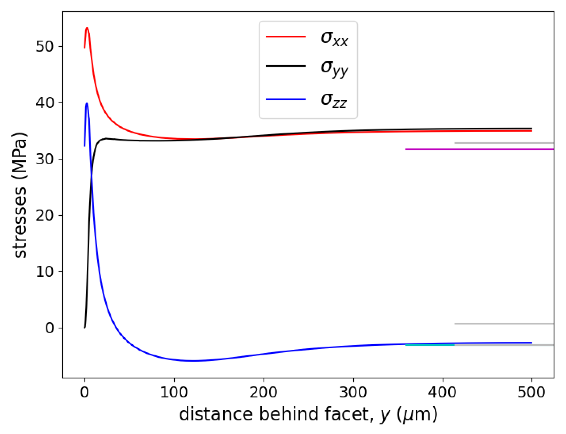
Figure 5 plots 3D estimations of the stresses owing to bonding strain as a function of the distance y behind the facet. The stresses are plotted for a line that is 5 μ m above the bonding surface (the bonding surface is the plane z = 98 μ m) and that is at the midpoint ( x = 0 ) of the chip. 2D FEM simulations are independent of y as the two dimensions considered are x and z. For a plane stress 2D FEM simulation, σ x x = 31.6 MPa, σ z z = 3.19 MPa, and σ y y = 0 MPa. The 2D plane strains values of σ x x = 32.8 MPa, σ z z = 3.11 MPa, and σ y y = 0.70 MPa are similar to the plane stress values. The long tic marks on the right-hand side of Figure 5 mark the stresses from the 2D plane strain (grey) and plane stress (magenta and cyan) approximations. The plots of the 2D values should extend for all values of y, but this makes the figure too cluttered.
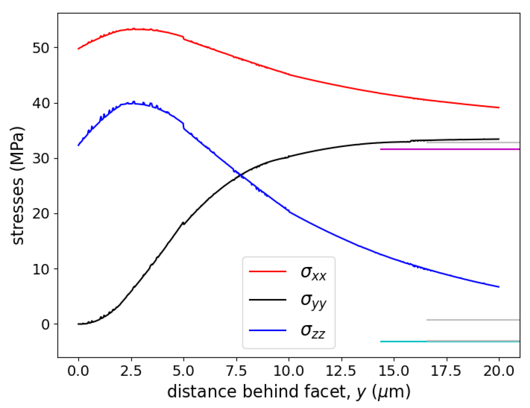
Figure 6 plots the same information as Figure 5 but on an expanded y scale and only near the facet, which occurs at y = 0 . Since the facet is assumed to be a free surface (the surface tractions are set equal to zero), the normal component of stress must equal zero, i.e., σ y y = 0 . The zoomed version of Figure 5 clearly shows that the 3D FEM simulation meets the boundary condition of σ y y = 0 at the facet, that the deformation of the sample is not uniform along the optic axis (i.e., the normal to the facet or y direction), and that this non-uniformity extends for a significant distance (>50 wavelengths) beyond the facet.
Note the ‘noise’ associated with the curves in Figure 6. This is the gridding, convergence, and interpolation noise mentioned in the discussion of the χ values for fits of 3D FEM simulations to the synthetic data, Table 2.
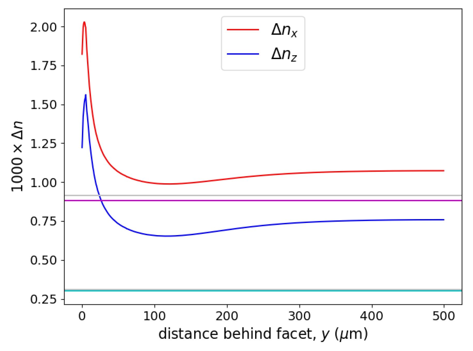
Figure 7 plots 2D and 3D estimates of the changes in the TE ( n x ) and TM ( n z ) refractive indices for a line 5 μ m above the bonding surface and in a plane perpendicular to the facet but at the midpoint of the chip. The 2D simulation and the 3D simulation at the midpoint (c.f. y 500 μ m for Figure 7) are similar in shape in that the 3D values approach a straight line at the midpoint of the chip but the magnitudes differ by up to >100%. The 2D predictions are indicated by straight lines as 2D simulations assume no y dependence in the material that is being simulated. The magenta-coloured line near 0.69 is 1000 × n x for a plane stress (2D) FEM simulation whereas the cyan coloured line near 0.26 is 1000 × n z for the same simulation. The grey lines are values obtained from a plane strain (2D) FEM simulation.
Figure 7 shows that there is little difference in the predicted photoelastic effect for a plane strain and a plane stress simulation, but there is a large discrepancy between the predicted strain-induced refractive index changes (i.e., photoelastic effect) for 3D and 2D FEM simulations.
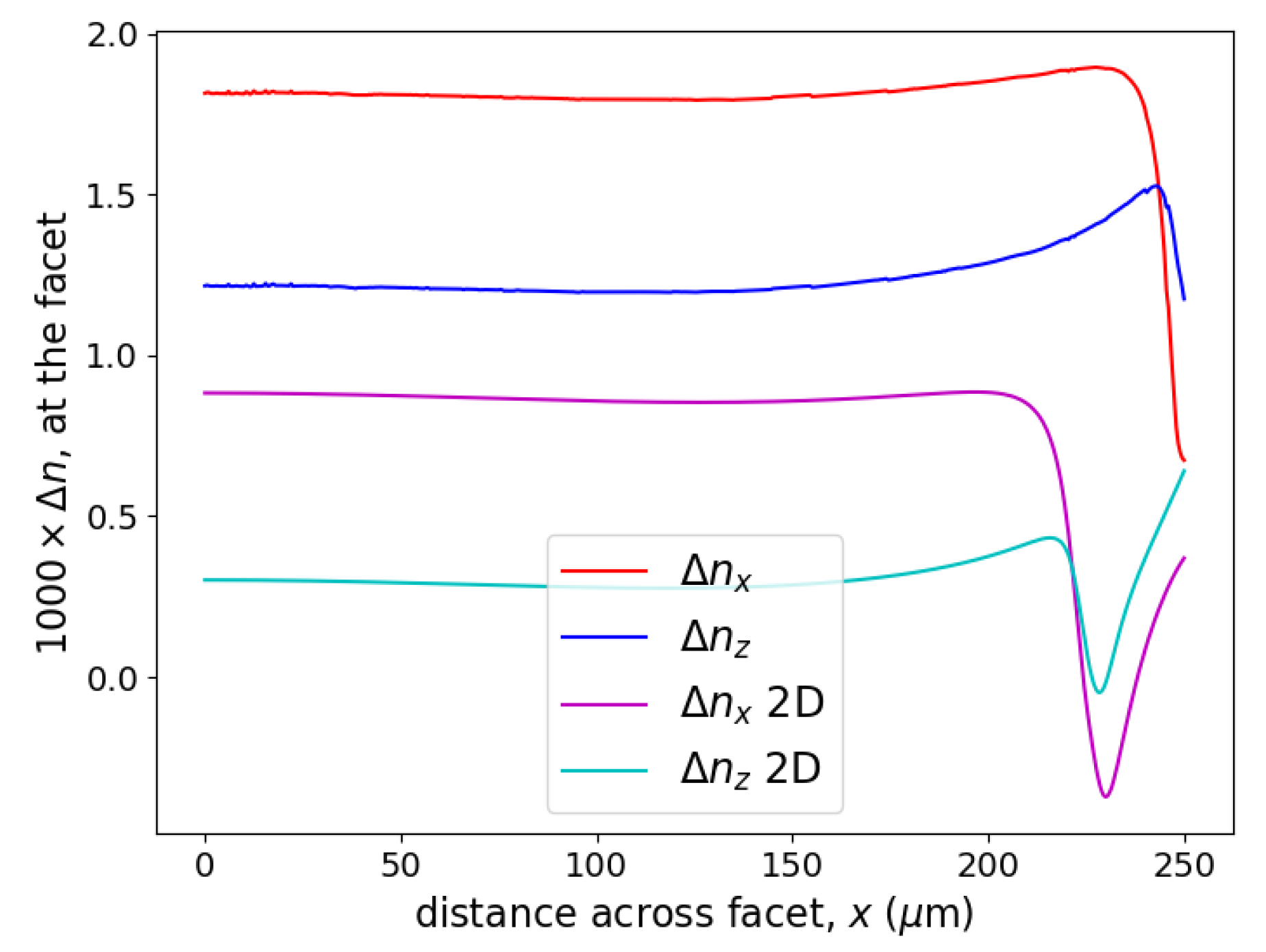
Figure 8 plots the estimated photoelastic index changes in the plane of the facet (i.e., the plane y = 0 ), from the bonding surface at z = 98 μ m to the top of the chip at z = 0 , and at mid-width ( x = 0 ) of the GaAs chip. For the 3D simulations, the refractive index changes, Δ n x and Δ n z , are ≈ 8 × 10 3 near the bonding surface and decrease rapidly as z increases from 98 μ m to say 90 μ m and then decrease slowly to the top of the chip.
Note that this chip was a specially prepared chip. There was no metal or dielectric coatings on the top surface at z = 0 . Any photoelastic effects from surface tractions on the top surface would add to the effects caused by the bonding. By the principle of linear superposition, one would expect any contribution from the top surface to add linearly as the FEM model is a linear model of elasticity. This sample is somewhat ideal for this investigation in the sense that the simple boundary conditions remove some degrees of freedom and hence simplify explanations and modelling.
The plane stress 2D FEM simulation show that the 2D photoelastic predictions are similar to the 3D predictions far away from the bonding surface but deviate substantially from the 3D predictions within about 15 μ m from the bonding surface. This behaviour is similar to stresses in Figure 6 and the refractive index changes when plotted along y, as shown in Figure 7.
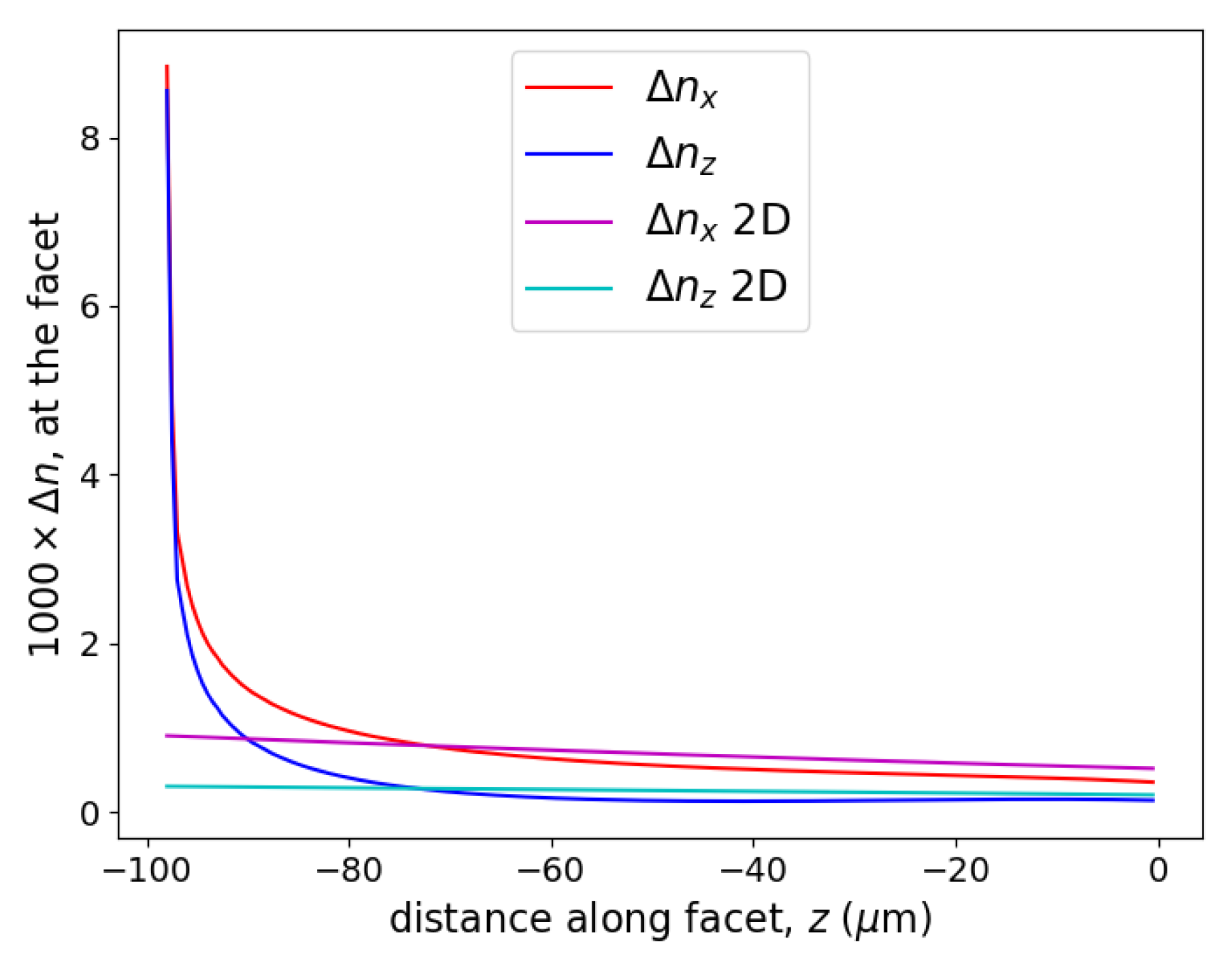
Figure 9 plots the 2D and 3D photoelastic effects in the plane of the facet (i.e., the y = 0 plane) from the mid-width at x = 0 to the edge of the chip at x = 250.5 μ m. The data are plotted for a line that is 5 μ m above the bonding surface. The 2D FEM photoelastic predictions are smaller in magnitude that the 3D FEM photoelastic predictions and are significantly different than the 3D predictions near the free surface at x = 250.5 μ m, which is the side wall on the right-hand-side of the chip. These differences between the 2D and 3D predictions near a surface are consistent with the results presented in Figure 7 and Figure 8, and the stresses presented in Figure 5 and Figure 6.

3. Conclusions

Two dimensional (2D) and three dimensional (3D) finite element method (FEM) simulations of the degree of polarisation (DOP) and of the rotated degree of polarisation (ROP) were fit to measurements of the DOP and ROP of photoluminescence (PL) (see Equation (1)) from a facet of a GaAs laser that was soldered to a sub-mount. The soldering to a submount induces deformation in the laser chip, and this deformation causes distinct patterns in the DOP and ROP.
Fits to the distinct patterns in the DOP and ROP of luminescence provides a method to deduce the strain in luminescencent III–V materials by fits of simulations to the measured data. Since the DOP and ROP for III–V materials are highly sensitive functions of shear strain and of the difference of the normal components of strain (see Equation (2)), the presence of shear strains and differences of normal components of strain ≳ 5 × 10 5 can be established and analysed by fitting simulations to the measured DOP and ROP patterns. A strain value of 5 × 10 5 is well above the typical noise floor.
It was shown through fits of FEM simulations to synthetic DOP and ROP data, which were created by 3D FEM simulations using deformations calibrated by the fits to experimental data, that the 2D FEM simulations do not fit the facet data well. Thus deformations (i.e., strains or the stresses causing the strains) obtained by 2D analyses of facet DOP data might not represent well the true state of deformation of the sample under study. This lack of representation is particularly acute within ≈ 20 μ m of free or loaded surfaces.
The deformations obtained by fits to measured data were used to predict the strain-induced changes (or photoelastic effects) for two orthogonal refractive indices. It was found that the 2D FEM simulations did not predict the photoelastic effect well, which is consistent with the ability of the 2D methods to predict the deformation.
Although 2D FEM simulations and analytic methods require significantly less computer resources than 3D FEM methods, it is recommended that the 2D methods be used to provide starting points for 3D FEM investigations. This is particularly true when results are required for distances close (say within 50 wavelengths or more) to surfaces.

Funding

This research received no external funding.

Data Availability Statement

The raw data supporting the conclusions of this article will be made available on request.

Conflicts of Interest

The author declares no conflicts of interest.

Appendix A. Stress and Strain

This Appendix provides an overview of linear elastic theory, a summary of notation, and the origin of the elastic constants used in the simulations and the other Appendices.
Stress σ and strain e, which are symmetric, three dimensional (3D), second-rank tensors, are related to each other by fourth rank compliance s and stiffness c tensors [14] (p. 132):
e i j = s i j k l σ k l = k , l s i j k l σ k l
σ i j = c i j k l e k l = k , l c i j k l e k l ,
with i = 1 . . . 3 , j = 1 . . . 3 , k = 1 . . . 3 , and l = 1 . . . 3 . The Einstein convention of summation over repeated indices is explicitly indicated by the sums on the right hand sides of Equations (A1) and (A2) [14] (p. 7).
Tensors are defined based on how components of the tensor transform under rotation of the underlying coordinate system [14] (p. 14). Both symmetric, 3D, second-rank tensors and the coefficients of a quadric transform the same under rotation of the underlying coordinate system. Thus, the components of stress and strain tensors can be written as symmetric 3 × 3 matrices and a quadric provides a means to visualize symmetric, second rank tensors.
A quadric is a second degree surface, such as m , n A m n x m x n = A m n x m x n = 1 , m = 1 . . . 3 , n = 1 . . . 3 , and with A m n = A n m , where the three mutually orthogonal variables are x 1 , x 2 , x 3 . The coefficients A m n of a quadric form a symmetric 3 × 3 matrix [14] (p. 16). For a symmetric, 3D second-rank Cartesian tensor T, T m n x m x n = ± 1 where the sign is the same as the sign of the determinant of the matrix representation of T [26] (p. 35).
The properties of quadrics, such as transformation, principal axes, eigenvalues, eigenvectors, and principal invariants, which are the trace, the determinate, and A 11 A 22 + A 22 A 33 + A 11 A 33 A 12 2 A 23 2 A 13 2 , are known. Thus, by analogy, the properties of symmetric, second-rank tensors are also known.
To minimise the number of subscripts, the components of stress and strain tensors can be written in matrix form using a Voigt notation. In Voigt notation the components of the strain tensor e are written with a single subscript and are given by
e = e 1 e 6 e 5 e 6 e 2 e 4 e 5 e 4 e 3 = e x x e x y e x z e x y e y y e y z e x z e y z e z z = e 11 e 12 e 13 e 12 e 22 e 23 e 13 e 23 e 33 .
The last two matrices in Equation (A3) give the components of the strain tensor e in x , y , z and x 1 , x 2 , x 3 Cartesian coordinate systems.
It is common practice to write the stress and strain relations in a matrix form, with the stiffness matrix [ C ] and the compliance matrix [ S ] being 6 × 6 matrices [14] (p. 134). [ e ] = [ S ] [ σ ] , [ σ ] = [ C ] [ e ] , and [ C ] and [ S ] are matrix inverses: [ C ] = [ S ] 1 and [ S ] = [ C ] 1 . The strain matrix [ e ] is [ e 1 , e 2 , e 3 , 2 e 4 , 2 e 5 , 2 e 6 ] T whereas the stress matrix [ σ ] is [ σ 1 , σ 2 , σ 3 , σ 4 , σ 5 , σ 6 ] T , so that
σ 1 σ 2 σ 3 σ 4 σ 5 σ 6 = C 11 C 12 C 13 0 0 0 C 12 C 22 C 23 0 0 0 C 13 C 23 C 33 0 0 0 0 0 0 C 44 0 0 0 0 0 0 C 55 0 0 0 0 0 0 C 66 e 1 e 2 e 3 2 e 4 2 e 5 2 e 6 .
The engineering shear strains are γ 4 = 2 e 4 , γ 5 = 2 e 5 , and γ 6 = 2 e 6 where e 4 , e 5 , and e 6 are the tensor shear strains. The engineering shear strains equal the decrease in angle between two lines that were perpendicular prior to application of the influence that induced the deformation [14] (p. 102).
The matrix representations of fourth rank compliance and stiffness tensors do not transform under rotation of the coordinate axes the same as fourth rank tensors [14] (p. 135). One must return to the tensor notation to find the components of the matrix representations of the compliance and stiffness tensors in a rotated coordinate system. Symmetric second rank tensors transform the same as the matrix representation of the tensor [14] (p. 102).
For a cubic crystal such as InP or GaAs, and in the crystal coordinate system, the components of the stiffness matrix [ C ] are
[ C ] = C 11 C 12 C 12 0 0 0 C 12 C 11 C 12 0 0 0 C 12 C 12 C 11 0 0 0 0 0 0 C 44 0 0 0 0 0 0 C 44 0 0 0 0 0 0 C 44
and the components of the compliance matrix [ S ] are, since [ S ] = [ C ] 1 ,
[ S ] = S 11 S 12 S 12 0 0 0 S 12 S 11 S 12 0 0 0 S 12 S 12 S 11 0 0 0 0 0 0 S 44 0 0 0 0 0 0 S 44 0 0 0 0 0 0 S 44
with
S 11 = C 11 + C 12 C 11 C 12 C 11 + 2 C 12 S 12 = C 12 C 11 C 12 C 11 + 2 C 12 S 44 = 1 C 44 .
For GaAs, the three independent coefficients in the crystal coordinate system are C 11 = 118 ± 0.4 GPa, C 12 = 53.5 ± 1.5 GPa, and C 44 = 59 ± 0.2 GPa [27].
In the facet coordinate system, which is obtained by a 45 deg rotation about the crystal coordinate z or ‘3’ axis, the stiffness matrix is (from rotation of the tensor)
( C 11 + C 12 ) / 2 + C 44 ( C 11 + C 12 ) / 2 C 44 C 12 0 0 0 ( C 11 + C 12 ) / 2 C 44 ( C 11 + C 12 ) / 2 + C 44 C 12 0 0 0 C 12 C 12 C 11 0 0 0 0 0 0 C 44 0 0 0 0 0 0 C 44 0 0 0 0 0 0 ( C 11 C 12 ) / 2
which we write as
[ c ] = c 11 c 12 c 13 0 0 0 c 12 c 11 c 13 0 0 0 c 13 c 13 c 33 0 0 0 0 0 0 c 44 0 0 0 0 0 0 c 44 0 0 0 0 0 0 c 66
with c 11 = ( C 11 + C 12 ) / 2 + C 44 , c 12 = ( C 11 + C 12 ) / 2 C 44 , c 13 = C 12 , c 44 = C 44 , and c 66 = ( C 11 C 12 ) / 2 .
The compliance matrix in the facet coordinate system is
[ s ] = s 11 s 12 s 13 0 0 0 s 12 s 11 s 13 0 0 0 s 13 s 13 s 33 0 0 0 0 0 0 1 / C 44 0 0 0 0 0 0 1 / C 44 0 0 0 0 0 0 2 / ( C 11 C 12 )
with
s 11 = C 11 2 + C 11 C 12 + 2 C 11 C 44 2 C 12 2 4 C 44 C 11 2 + C 11 C 12 2 C 12 2 s 12 = C 11 2 + C 11 C 12 2 C 11 C 44 2 C 12 2 4 C 44 C 11 2 + C 11 C 12 2 C 12 2 s 13 = C 12 C 11 2 + C 11 C 12 2 C 12 2 s 33 = C 11 + C 12 C 11 2 + C 11 C 12 2 C 12 2 .
In a facet coordinate system and for GaAs
[ c ] GaAs = 144.75 26.750 53.5 0 0 0 26.750 144.75 53.5 0 0 0 53.5 53.5 118 0 0 0 0 0 0 59 0 0 0 0 0 0 59 0 0 0 0 0 0 32.250 GPa
[ s ] GaAs = 8303 172 3686 0 0 0 172 8303 3686 0 0 0 3686 3686 11817 0 0 0 0 0 0 16949 0 0 0 0 0 0 16949 0 0 0 0 0 0 31008 × 10 6 GPa
It is common in engineering to write the relations in terms of Young’s modulus E and Poisson’s ratio ν . The relations can be written in two different formats: the major Poisson format (or row normalized format)
e x x = 1 E x σ x x ν ¯ x y σ y y ν ¯ x z σ z z
and the minor Poisson format (or column normalized format)
e x x = σ x x E x ν x y σ y y E y ν x z σ z z E z .
The standard relation for shear strain, regardless of Poisson format, is
γ x y = 2 e x y = σ x y G x y
where G x y is the rigidity modulus, γ x y is the engineering shear strain, and e x y is the tensor shear strain. G = E / ( 2 × ( 1 + ν ) ) in isotropic material.
Similar equations hold for e y y , e z z , e y z , and e x z .
The GaAs constants in major and minor Poisson format, and in a facet coordinate system, are
E x = 1 / s 11 = 120.44 ν ¯ x y = s 12 / s 11 = 0.021 ν ¯ x z = s 13 / s 11 = 0.444 E y = 1 / s 22 = 120.44 ν ¯ y x = s 21 / s 22 = 0.021 ν ¯ y z = s 23 / s 22 = 0.444 E z = 1 / s 33 = 84.62 ν ¯ z x = s 31 / s 33 = 0.312 ν ¯ z y = s 32 / s 33 = 0.312 G x y = 1 / s 66 = 32.25 G x z = 1 / s 55 = 59.00 G y z = 1 / s 44 = 59.00
and
E x = 1 / s 11 = 120.44 E y = 1 / s 22 = 120.44 E z = 1 / s 33 = 84.62 ν x y = s 12 / s 22 = 0.021 ν x z = s 13 / s 33 = 0.312 ν y x = s 21 / s 11 = 0.021 ν y z = s 23 / s 33 = 0.312 ν z x = s 31 / s 11 = 0.444 ν z y = s 32 / s 22 = 0.444 G x y = 1 / s 66 = 32.25 G x z = 1 / s 55 = 59.00 G y z = 1 / s 44 = 59.00
respectively.

Appendix B. Photoelasticity

Nye [14] (Ch. XIII Section 2.2) explains that strain affects the refractive index and that this is modelled from changes to the relative dielectric impermeabilities, B i , i = 1 . . . 6 , in matrix notation. The refractive indices are related to the impermeabilities by B i = n i 2 , i = 1 . . . 3 .
Before symmetric material is deformed, the indicatrix is a sphere, B o x i x i = 1 with B o = 1 / n o 2 where n o is the refractive index of the unstrained material [14,15]. For GaAs, a value of n o = 3.521 was assumed. After deformation, the indicatrix is B i j x i x j , which in general is an ellipse. The off diagonal elements of B i j , are related to shear deformation in the material. If the shear is non-zero, then the principal axes of the indicatrix do not align with the ( x 1 , x 2 , x 3 ) Cartesian coordinate system. Propagation of light in material with non-zero shear can lead to a rotation of the plane of polarisation [20,21].
Strain induced changes in [ B ] are given by
Δ B i = p i j e j = π i j σ j
and the changes in refractive index are given by
Δ n i = n o 3 Δ B i 2 , i = 1 . . . 3 .
In the crystal coordinate system and in matrix notation, measured values for the three unique GaAs elasto-optical coefficients of the fourth rank photo-elastic tensor are P 11 = 0.165 , P 12 = 0.140 , and P 44 = 0.072 at a wavelength of 1.15 μ m [17,18]. Similar to the use of c and C for the stiffness constants (see Appendix A), here capital [ P ] represents the matrix of the elasto-optical coefficients in the crystal coordinate system and [ p ] refers to the matrix of the elasto-optical coefficients in the plane of the facet.
Tables 9 and 15 in Nye [14] (Ch. XIII Section 2.2) show that the photo-elastic matrix [ P ] for GaAs (GaAs has symmetry F 4 ¯ 3 m) has the same symmetry as the stiffness matrix [ C ] . Therefore, the [ p ] matrix in the plane of the facet can be found by substitution in Equation (A8).
In the plane of the facet and for GaAs,
[ p ] = 0.2245 0.0805 0.1400 0 0 0 0.0805 0.2245 0.1400 0 0 0 0.1400 0.1400 0.1650 0 0 0 0 0 0 0.0720 0 0 0 0 0 0 0.0720 0 0 0 0 0 0 0.0125
and using [ p ] = [ π ] [ c ] and [ π ] = [ p ] [ s ] , since [ s ] is the matrix inverse of [ c ] ,
[ π ] = 1.334 0.1137 0.5301 0 0 0 0.1137 1.334 0.5301 0 0 0 0.5301 0.5301 0.9177 0 0 0 0 0 0 1.2203 0 0 0 0 0 0 1.2203 0 0 0 0 0 0 0.3876 × 10 12 .
The expressions for [ p ] or [ π ] are used with Equations (A19) and (A20) to specify the photo-elastic response. If shear strain is present, then it might be necessary to take the shear-induced rotation of the indicatrix into account [19,20,21].
From the Kramers-Kronig relations, which follow from causality, the [ P ] and hence the Δ n are expected to be wavelength dependent, with magnitudes increasing as the wavelength of the light approaches the band gap from the wavelength at which the P were measured [16], [28] (p. 364), [29] (p. 93), and [30] (p. 360).

Appendix C. Plane Strain

Plane strain is an approximation to reduce a 3D problem to a 2D problem, wherein one assumes one principal component of strain is zero and two shear strains are zero.

Appendix C.1. Plane Strain in the Plane of the Facet

Adopt a facet coordinate system in which y is a normal to the facet, z is the vertical or growth direction, and x is the horizontal direction.
Assume e y y = 0 and e x y = e y z = 0 . The assumption that e y y = 0 places a constraint on σ y y :
σ y y = s 21 σ x x s 22 + s 23 σ z z s 22 .
Equation (A23) written in terms of the three stiffness constants from the crystal coordinate system is
σ y y = C 11 2 + C 12 + 2 C 44 C 11 + 2 C 12 2 C 11 2 + C 12 + 2 C 44 C 11 2 C 12 2 σ x x + 4 C 12 C 44 C 11 2 + C 12 + 2 C 44 C 11 2 C 12 2 σ z z .
For GaAs, σ y y = 0.0207 σ x x + 0.4440 σ z z for e y y = 0 .
Use Equation (A23) to eliminate σ y y from the 3D expressions for e x x and e z z to find
e x x = s 11 σ x x + s 12 σ y y + s 13 σ z z = s 11 s 12 s 21 s 22 σ x x + s 13 s 12 s 23 s 22 σ z z = 8302.75 3.563 σ x x + 3686.48 76.357 σ z z GaAs = 8299.19 σ x x 3762.77 σ z z GaAs
and
e z z = s 31 σ x x + s 32 σ y y + s 33 σ z z = s 31 s 32 s 21 s 22 σ x x + s 33 s 32 s 23 s 22 σ z z = 3686.48 76.357 σ x x + 11817.40 1636.348 σ z z GaAs = 3762.77 σ x x + 10180.58 σ z z GaAs
The numerical coefficients in Equations (A25) and (A26) must be multiplied by 10 6 given stresses in GPa.
Equations (A25) and (A26) can be written in matrix form:
e x x e z z = s 11 s 12 s 21 / s 22 s 13 s 12 s 23 / s 22 s 31 s 32 s 21 / s 22 s 33 s 32 s 23 / s 22 σ x x σ z z . .
For GaAs, by matrix inversion of Equations (A25) and (A26),
σ x x σ z z = 144.75 53.5 53.5 118.0 e x x e z z .
This result seems strange as it gives the same values for c x x , c x z , c z x , and c z z as before the plane strain changes—see Equation (A12) for the original values for [ c ] . The inverse of the 2 × 2 matrix in Equation (A28) is
[ s 2 D ] = 8299.19 3762.77 3762.77 10180.6 × 10 6 GPa ,
which is indeed the 2D compliance matrix, scaled by 10 6 (must multiply the values by 10 6 to get units of GPa 1 , as shown). This identification of Equation (A29) as the 2D compliance matrix [ s 2 D ] can be confirmed by comparing Equations (A25) and (A26) with Equation (A29).
To find plane strain values for E and ν when e y y = 0 , simply invert the 2D [ c ] matrix, which is found by deleting the y column and the y row, to find the 2D [ s ] matrix and use the components of the 2D [ s ] matrix to find values for E and ν . This approach is easier than the approach outlined in Appendix C.3.
Values for Poisson’s ratios for GaAs, as calculated from the inverse of the 2D [ c ] matrix, are
ν ¯ x z = s 2 D [ 1 , 2 ] s 2 D [ 1 , 1 ] = 3762.8 8299.2 = 0.45339 = ν z x ν ¯ z x = s 2 D [ 1 , 2 ] s 2 D [ 2 , 2 ] = 3762.8 8299.2 = 0.36960 = ν x z
These are the same values as found in Appendix C.3 for the major Poisson (row normalized) and the minor Poisson (column normalised) formats. The values for GaAs for E and G are also correct: E x = 1 / s 2 D [ 1 , 1 ] = 120.49 GPa and E z = 1 / s 2 D [ 2 , 2 ] = 98.226 GPa. The values for the rigidity G do not change.

Appendix C.2. Plane Strain Summary: Matrix Inversion

To find the plane strain material constants for e 22 = 0 , create a 2D stiffness matrix [ c 2 D ] by removing the y column and the y row from the 3D stiffness matrix [ c ] , i.e., form the c [ y , y ] minor [24] (p. 241), and remove the columns and rows associated with the shear terms. The matrix [ c ] is block diagonal in terms for the principal strains and the shear strain terms, and thus the principal strains and the shear strain are decoupled. Let
[ c 2 D ] = c 11 c 13 c 31 c 33
then
[ c 2 D ] 1 = [ s 2 D ] = c 33 c 11 c 33 c 13 c 13 c 13 c 11 c 33 c 13 c 13 c 31 c 11 c 33 c 13 c 13 c 11 c 11 c 33 c 13 c 13
and
ν ¯ 13 = s 2 D [ 1 , 2 ] s 2 D [ 1 , 1 ] = c 13 c 33 = 53.5 118.0 = 0.45339 = ν 31 ν ¯ 31 = s 2 D [ 2 , 1 ] s 2 D [ 2 , 2 ] = c 31 c 11 = 53.5 144.75 = 0.36960 = ν 13 ,
in agreement with values calculated earlier, Equation (A30).

Appendix C.3. The Hard Way

In the major Poisson format, the plane strain condition at a facet is e y y = 0 , which means σ y y = ν ¯ y x σ x x + ν ¯ y z σ z z . Substitute this relation into the expressions for the two non-zero strains to obtain
e x x = 1 E x σ x x ν ¯ x y σ y y ν ¯ x z σ z z = 1 E x σ x x 1 ν ¯ x y ν ¯ y x ν ¯ x y ν ¯ y z + ν ¯ x z σ z z 1 ν ¯ x y ν ¯ y x E x σ x x ν ¯ x y ν ¯ y z + ν ¯ x z 1 ν ¯ x y ν ¯ y x σ z z
e z z = 1 E z ν ¯ z x σ x x ν ¯ z y σ y y + σ z z = 1 E z ν ¯ z x + ν ¯ z y ν ¯ y x σ x x + 1 ν ¯ z y ν ¯ y z σ z z
which would suggest for GaAs that
E x E x 1 ν ¯ x y ν ¯ y x = E x 1 0.021 × 0.021 = 1.0004 E x ν x z ν ¯ x y ν ¯ y z + ν ¯ x z 1 ν ¯ x y ν ¯ y x = 0.021 × 0.444 + 0.444 1 0.021 × 0.021 = 0.4534 E z E z 1 ν ¯ z y ν ¯ y z = E z 1 0.312 × 0.444 = 1.1608 E z ν z x ν ¯ z x + ν ¯ z y ν ¯ y x 1 ν ¯ z y ν ¯ y z = 0.312 + 0.312 × 0.021 1 0.312 × 0.444 = 0.3696
if using the major Poisson format (row normalized) for plane strain with e y y = 0 . The symbols to the left of the arrow would be used in Equation (A14) and the expression for e z z that is obtained by replacing x with z in (A14).
For a minor Poisson format (column normalized),
e x x = σ x x E x ν x y σ y y E y ν x z σ z z E z = σ x x 1 ν x y ν y x E x ν x y ν y z + ν x z 1 ν z y ν y z σ z z 1 ν z y ν y z E z
e z z = ν z x σ x x E x ν z y σ y y E y + σ z z E z = ν z y ν y x + ν z x 1 ν x y ν y x σ x x 1 ν x y ν y x E x + σ z z 1 ν z y ν y z E z
which would suggest for GaAs that
E x E x 1 ν x y ν y x = E x 1 0.021 × 0.021 = 1.0004 E x ν x z ν x y ν y z + ν x z 1 ν z y ν y z = 0.021 × 0.312 + 0.312 1 0.444 × 0.312 = 0.3696 E z E z 1 ν z y ν y z = E z 1 0.444 × 0.312 = 1.1608 E z ν z x ν z y ν y x + ν z x 1 ν x y ν y x = 0.444 × 0.021 + 0.444 1 0.021 × 0.021 = 0.4534
if using the minor Poisson format (column normalised) for plane strain with e y y = 0 . The symbols to the left of the arrow would be used in Equation (A15) and the expression for e z z that is obtained by replacing x with z in (A15).
It is a lot less work to calculate a 2D matrix inverse to find E and ν !

Appendix C.4. 3D Limit

The plane strain constants can be found from the inverse of the 3D stiffness matrix.
Consider a stiffness matrix g in a facet coordinate system:
g = g 11 g 12 g 13 g 12 g 11 g 13 g 13 g 13 g 33 .
The inverse of this matrix is
1 D g 33 g 11 g 13 2 g 33 g 12 g 13 2 g 13 g 11 g 12 g 33 g 12 g 13 2 g 33 g 11 g 13 2 g 13 g 11 g 12 g 13 g 11 g 12 g 13 g 11 g 12 g 11 g 12 g 11 + g 12
with the determinant D = g 11 g 12 g 33 g 11 + g 33 g 12 2 g 13 g 13 .
Assume plane strain with the z component = 0. Take the limit of the g 1 [ z , z ] minor [24] (p. 241) as g 33 0 and g 13 0 . In this limit, the 2 × 2 submatrix (or g 1 [ z , z ] minor) is
g 11 ( g 11 + g 12 ) g 11 g 12 g 12 ( g 11 + g 12 ) g 11 g 12 g 12 ( g 11 + g 12 ) g 11 g 12 g 11 ( g 11 + g 12 ) g 11 g 12 ,
which is equal to the 2D compliance matrix, i.e, the limit is equal to the matrix inverse of the 2 × 2 stiffness matrix formed by removing the z row and z column of Equation (A41). Thus one can find the 2D stiffness or compliance matrix by taking the limit of the 2 × 2 g 1 [ z , z ] minor of the inverse of the 3D compliance or stiffness matrix as the z terms go to zero.

Appendix D. Plane Stress in the Plane of a Facet

Adopt a facet coordinate system in which y is a normal to the facet, z is the vertical or growth direction, and x is the horizontal direction and in the plane of the facet.
Assume that the facet is a free surface and thus σ y y = 0 and σ x y = σ y z = 0 . The assumption that σ y y = 0 places a constraint on e y y :
e y y = c 21 e x x e 22 + c 23 e z z c 22 .
Use Equation (A43) to eliminate e y y from the 3D expressions for σ x x and σ z z to find
σ x x = c 11 e x x + c 12 e y y + c 13 e z z = c 11 c 12 c 21 c 22 e x x + c 13 c 12 c 23 c 22 e z z = 147.65 4.9434 e x x + 53.5 9.8869 e z z GaAs = 139.81 e x x + 43.6131 e z z GaAs
and
σ z z = c 31 e x x + c 32 e y y + c 33 e z z = c 31 c 32 c 21 c 22 e x x + c 33 c 32 c 23 c 22 e z z = 53.5 9.8869 e x x + 118 19.7737 e z z GaAs = 43.6131 e x x + 98.2263 e z z GaAs
Equations (A44) and (A45) can be set in matrix form (the numerical values are for GaAs):
σ x x σ z z = 139.8065630 43.61312608 43.61312608 98.22625216 e x x e z z
The inverse of the 2D stiffness matrix in Equation (A46) is
[ s 2 D ] = 8302.75 3686.48 3686.48 11817.40 × 10 6 GPa .
The compliance values in [ s 2 D ] are the same as the corresponding values in the original 3D compliance matrix [ s ] , which is displayed as Equation (A13). If a 2D compliance matrix is created from the s [ y , y ] minor [24] (p. 241) of [ s ] by removing the y columns and rows, and the matrix inverse of this 2D compliance matrix [ s 2 D ] is obtained, then the plane stress adjusted stiffness matrix from Equations (A44) and (A45) is obtained. This is demonstrated below, where s i j are components from the 3D compliance matrix in the plane of the facet and for GaAs, Equation (A13). As usual, x and ‘1’ label the same direction, y and ‘2’ label the same direction, and z and ‘3’ label the same direction.
s 11 s 13 s 31 s 33 1 = 139.8065630 43.61312608 43.61312608 98.22625216 = [ c 2 D ]
Summary: Plane Strain and Plane Stress
For ξ = x or ξ = y or ξ = z :
the plane strain constants for e ξ ξ = 0 can be found from the c [ ξ , ξ ] minor [24] (p. 241) of the 3D stiffness matrix [ c ] . The corresponding compliance matrix [ s ] is found as the inverse of the c [ ξ , ξ ] minor of the 3D stiffness matrix [ c ] ;
and,
the plane stress constants for σ ξ ξ = 0 can be found from the s [ ξ , ξ ] minor [24] (p. 241) of the 3D compliance matrix [ s ] . The corresponding stiffness matrix [ c ] is found as the inverse of the s [ ξ , ξ ] minor of the 3D compliance matrix [ s ] .
The plane strain or plane stress constants can also be found by taking the limit, as the ξ components equal zero, of the ( ξ , ξ ) minor of the matrix inverse of the appropriate 3D matrix, as demonstrated in Appendix C.4.

References

  1. Kirkby, P.A.; Selway, P.R.; Westbrook, L.D. Photoelastic waveguides and their effect on stripe-geometry GaAs/Ga1−xAlxAs lasers. J. Appl. Phys. 1979, 50, 4567–4579. [Google Scholar] [CrossRef]
  2. Saada, A.S. Elasticity Theory and Application; Robert E Krieger: Malabar, FL, USA, 1983. [Google Scholar]
  3. Hu, Y.Y.; Huang, W.M. Elastic and elastic-plastic analysis of multilayer thin films: Closed-form solutions. J. Appl. Phys. 2004, 96, 4154–4160. [Google Scholar] [CrossRef]
  4. Hsueh, C.H. Modeling of elastic deformation of multilayers due to residual stresses and external bending. J. Appl. Phys. 2002, 91, 9652–9656. [Google Scholar] [CrossRef]
  5. Hirth, J.P.; Lothe, J. Theory of Dislocations; McGraw Hill, Inc.: New York, NY, USA, 1968. [Google Scholar]
  6. Cassidy, D.T.; Lam, S.K.K.; Lakshmi, B.; Bruce, D.M. Strain mapping by measurement of the degree of photoluminescence. Appl. Opt. 2004, 43, 1811–1818. [Google Scholar] [CrossRef] [PubMed]
  7. Cassidy, D.T.; Landesman, J.P. Degree of polarization of luminescence from GaAs and InP as a function of strain: A theoretical investigation. Appl. Opt. 2020, 59, 5506–5520. [Google Scholar] [CrossRef]
  8. Adachi, S. Physical Properties of III-V Semiconductor Compounds InP, InAs, GaAs, GaP, InGaAs, and InGaAsP; Wiley: New York, NY, USA, 1992. [Google Scholar]
  9. Colbourne, P.D.; Cassidy, D.T. Imaging of stresses in GaAs diode lasers using polarization resolved photoluminescence. IEEE J. Quantum Electron. 1993, 29, 62–68. [Google Scholar] [CrossRef]
  10. Colbourne, P.D.; Cassidy, D.T. Bonding stress measurements from the degree of polarization of facet emission of AlGaAs superluminescent didoes. IEEE J. Quantum Electron. 1991, 27, 914–920. [Google Scholar] [CrossRef]
  11. Bahder, T.B. Eight-band k · p model of strained zinc-blende crystals. Phys. Rev. B 1990, 41, 11992–12001, Erratum in Phys. Rev. B 1992, 46, 9913. [Google Scholar] [CrossRef] [PubMed]
  12. Bahder, T.B. Analytic dispersion relations near the Γ point in strained zinc-blende crystals. Phys. Rev. B 1992, 45, 1629–1637. [Google Scholar] [CrossRef] [PubMed]
  13. Vurgaftman, I.; Meyer, J.R.; Ram-Mohan, L.R. Band parameters for III-V compound semiconductors and their alloys. J. Appl. Phys. 2001, 89, 5815–5875. [Google Scholar] [CrossRef]
  14. Nye, J.F. Physical Properties of Crystals; Oxford University Press: New York, NY, USA, 1985. [Google Scholar]
  15. Lovett, D.R. Tensor Properties of Crystals; Institute of Physics: London, UK, 1994. [Google Scholar]
  16. Adachi, S.; Oe, K. Internal strain and photelastic effects in Ga1−xAsx/GaAs and In1−xGaxAsyP1−y/InP crystals. J. Appl. Phys. 1983, 54, 6620–6627. [Google Scholar] [CrossRef]
  17. Suzuki, N.; Tada, K. Elastooptic and electrooptic properties of GaAs. Jpn. J. Appl. Phys. 1984, 23, 1011–1016. [Google Scholar] [CrossRef]
  18. Suzuki, N.; Tada, K. Elastooptic properties of InP. Jpn. J. Appl. Phys. 1983, 22, 441–445. [Google Scholar] [CrossRef]
  19. Hempel, M.; Ziegler, M.; Schwirzke-Schaaf, S.; Tomm, J.W.; Jankowski, D.; Schroeder, D. Spectroscopic analysis of packaging concepts for high-power diode laser bars. Appl. Phys. A—Mater. Sci. Process. 2012, 107, 371–377. [Google Scholar] [CrossRef]
  20. Cassidy, D.T.; Rehioui, O.; Hall, C.K.; Béchou, L.; Deshayes, Y.; Kohl, A.; Fillardet, T.; Ousten, Y. High-power laser bars and shear strain. Opt. Lett. 2013, 38, 1633–1635. [Google Scholar] [CrossRef] [PubMed]
  21. Cassidy, D.T. Rotation of principal axes and birefringence in III–V lasers owing to bonding strain. Appl. Opt. 2013, 52, 6258–6265. [Google Scholar] [CrossRef] [PubMed]
  22. Cassidy, D.T.; Landesman, J.P. Degree of polarization of luminescence from InP under SiN stripes: Fits to FEM simulations. Opt. Contin. 2023, 2, 1505–1522. [Google Scholar] [CrossRef]
  23. FlexPDE 7 Users Manual 2023. Available online: https://www.pdesolutions.com/download/flexpde-722-user-manual.pdf (accessed on 14 August 2024).
  24. Kreyszig, E. Advanced Engineering Mathematics, 3rd ed.; John Wiley and Sons: New York, NY, USA, 1972. [Google Scholar]
  25. Bevington, P.R.; Robinson, D.K. Data Reduction and Error Analysis for the Physical Sciences, 2nd ed.; McGraw Hill, Inc.: New York, NY, USA, 1992. [Google Scholar]
  26. Byron, F.W.; Fuller, R.W. Mathematics of Classical and Quantum Physics, revised ed.; Dover Books on Physics: Sacramento, CA, USA, 1992. [Google Scholar]
  27. Dunstan, D.J. Stiffness of GaAs. In Properties of Gallium Arsenide, 3rd ed.; Brozel, M.R., Stillman, G.E., Eds.; Inspec: London, UK, 1996. [Google Scholar]
  28. Bracewell, R.N. The Fourier Transform and Its Applications, 3rd ed.; McGraw-Hill Companies: New York, NY, USA, 2000. [Google Scholar]
  29. Born, M.; Wolf, E. Principles of Optics, 6th (corrected) ed.; Cambridge University Press: Cambridge, UK, 1993. [Google Scholar]
  30. Weissbluth, M. Photon-Atom Interactions; Academic Press, Inc.: San Diego, CA, USA, 1989. [Google Scholar]
Figure 1. Maps of the degree of polarisation (DOP) and rotated degree of polarisation (ROP) in the vicinity of waveguides. The ROP and DOP would be zero in the absence of an anisotropic strain. The inset shows schematically the surface relief and overlayers (in green and yellow) that exist on the top surface of the sample and that cause the measured DOP and ROP patterns.
Optics 06 00021 g001
Figure 2. Schematic diagrams of the sample. The diagrams show the measurement coordinate systems and the crystal coordinate systems in the plane of the facet and in the top surface.
Optics 06 00021 g002
Figure 3. 3D grid with 400 × deformations in the horizontal ( x ) and vertical (z) directions and at a facet for the GaAs chip. The left boundary is an x = 0 plane and is a plane of symmetry; only the right-hand half of the chip was simulated. The red lines show the boundaries of the chip before deformation, and have lengths of 250.5 μ m in the x (horizontal) direction and 98 μ m in the z (vertical) direction.
Optics 06 00021 g003
Figure 4. False colour images the PL data, the measured DOP and ROP data, and of best fit functions to the measured DOP and ROP. For display purposes the aspect ratio has not been maintained; the maps should be ≈5× wider than the maps are to maintain the aspect ratio. The dimensions of each panel are 513 μ m in the horizontal directions and 105 μ m in the vertical direction.
Optics 06 00021 g004
Figure 5. Stresses as calculated from a 3D FEM simulation of the bonded chip. The stresses are presented along a line that is 5 μ m above the bonding surface and for x = 0 . Data for only one half of the chip are plotted; the plane y = 500 μ m is a plane of symmetry.
Optics 06 00021 g005
Figure 6. Stresses as calculated from a 3D FEM simulation of the bonded chip and displayed with an expanded y axis to highlight the changes along the y-axis. The stresses are presented along a line that is 5 μ m above the bonding surface and at the mid-width ( x = 0 ) of the chip. The long tic marks on the right-hand side indicate the stresses from the 2D plane strain (grey) and plane stress (magenta and cyan) approximations.
Optics 06 00021 g006
Figure 7. 2D (horizontal lines) and 3D predictions of the changes in the refractive indices along the length of the device, 5 μ m above the bonding surface, and in a plane x = 0 , which is perpendicular to the facet and at the mid-width of the chip.
Optics 06 00021 g007
Figure 8. 2D and 3D predictions of the changes in the refractive indices at the facet, from the bonding surface at z = 98 μ m to the top of the chip at z = 0 for a line along x = 0 . The plane x = 0 is at the mid-width of the chip and is a plane of symmetry.
Optics 06 00021 g008
Figure 9. 2D and 3D predictions of the changes in the refractive indices at the facet and as a function of x, for 5 μ m above the bonding surface. x = 0 μ m is a plane of symmetry.
Optics 06 00021 g009
Table 1. χ values for fits of 2D and 3D FEM simulations to measured DOP and ROP data.
Method χ T χ DOP χ ROP R ( m ) e / 10 4
3D 3.31 3.23 3.39 0.59 3.11
2D plane stress 3.157 ± 0.01 3.160 3.154 0 . 75 0.22 + 0.55 3.80 ± 0.4
2D plane strain 3.165 3.163 3.168 0.64 3.91
Table 2. χ values for fits of 2D and 3D FEM simulations to synthetic data.
Method χ T χ DOP χ ROP R ( m ) e / 10 4
3D 0.004 0.003 0.004 0.612 3.059
2D plane stress 0.984 ± 0.01 0.968 1.001 1 . 2 0.35 + 0.2 2.85 ± 0.2
2D plane strain 0.969 0.956 0.982 1.2 2.85
Disclaimer/Publisher’s Note: The statements, opinions and data contained in all publications are solely those of the individual author(s) and contributor(s) and not of MDPI and/or the editor(s). MDPI and/or the editor(s) disclaim responsibility for any injury to people or property resulting from any ideas, methods, instructions or products referred to in the content.

