Abstract
In the design of photonic integrated circuits (PICs), the optical connections of the PIC surface, along with the electronic components of the chips, are significant issues. One of the optoelectronics components that utilizes these surface connections are electro-reflective modulators, consisting of an optical section and an electronic section. In this paper, a novel scheme of two-dimensional photonic crystals (PhCs) is presented for the optical and reflective sections of this device. This design is two-dimensional; thus, it has less volume than the current bulky structures. The finite element method is utilized to simulate and optimize the scheme of PhCs and gold layer parameters. Furthermore, optimization of design parameters is accomplished through the Nelder–Mead method. Moreover, the modeling and simulation of the proposed hybrid PhCs has been investigated according to the structural parameters with tolerance. These tolerances, related to the nanorods’ radius and lattice constants, are considered to justify and vindicate the fabrication technology limitations and conditions. In the “on” state of the modulator, the light transmission ratio is 98% for a 903 nm wavelength with a 45° angle of deflection and incident light, nd the bandwidth is 20 nm. For an 897 nm wavelength with a 41° angle, the transmission ratio is 95%, and the bandwidth is 7 nm.
1. Introduction
Several schematic designs and applications are shown for the surface optical connections to electronic circuits of integrated chips in Figure 1a, including the coupling of two internal parts of an optical integrated circuit (OIC) and the linking of two segregated OICs. One of the candidate technologies for these connections is silicon photonics (SiP), which uses CMOS processes to connect electronic chips through multi-level integration [,]. Recently, a seamless hybrid-integrated interconnected network architecture has been proposed that employs an “optical bridge” platform comprising flexible polymer ribbon waveguide arrays integrated with three to five active devices for the optical interconnections between Si CMOS chips co-packaged with the optical components.
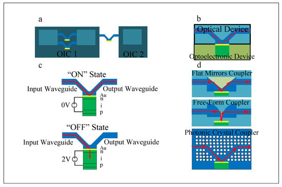
Figure 1.
The illustrations are schematics. (a) Applications of the electro-reflective modulators in the interconnections of an OIC and the optical connection between two OICs. (b) The top section shows the optical component, and the bottom section shows the electronic component of this modulator. (c) The operation of the “on” and “off” states of the device is illustrated. (d) The optical section of the modulator shows the flat reflector, parabolic reflector, and PhCs.
As an alternative to planar waveguide integration of photonic components in SiP, the optical bridge integrates compact and efficient surface-incident active photonic components with single-mode flexible polymer waveguides through freeform optical couplers []. Many optoelectronic devices use a surface-incident configuration to facilitate coupling with light emitted to or from free space []. Examples of such devices include vertical cavity surface-emitting lasers, multi-quantum-well (MQW) modulators, and free-space photodetectors []. In the multimode regime, flat and curved mirrors, prism couplers, and facet couplers have been implemented to couple light from or to these surface-incident devices [].
These connections are made through optical reflectors from the chip surface to electronic components such as optical detectors or laser active sources of chips. Direct coupling of light from an optical waveguide on a chip to a second waveguide on another chip is a useful and effective function for interfacing photonic chips or coupling light from chips to optical printed circuit boards (PCBs) [,,,,,].
Such interconnection has been traditionally performed with 45° mirrors [,,,] or grating couplers []. The surface reflectors act to bend light based on the difference between the refractive index of waveguide and air; therefore, they can direct light to another surface at any angle. These reflectors are initially considered flat; however, after shape optimization, they are parabola shaped. The three-dimensional parabola that focuses light at its focal point is created by the process of making two-photon polymers (TPP); however, recent advances in parallel TPP printing promise significant advances in the production of 3D free-form reflectors [,]. Instances of photonic structures utilizing TPP include the fabrication of microneedle arrays [], three-dimensional photonic crystals [,,,], photonic wire bonding [,,], multi-lens objectives [,] free-form optics and coupling [,], and fiber to waveguide connector [].
In this article, the electronic section of chip is a p-i-n diode with an intrinsic region comprising MQWs GaAs/AlGaAs layers. On–off modulators can be made by combining the optical reflector part at the optical surface and this diode. This design presents more effective specifications than the ones in the conventional designs, i.e., the electro-optical modulators and electro-absorption modulators [].
The modulators consist of an optical section and an electronic section (Figure 1b). A gold layer is used to reflect light in the “on” state of the modulator. This layer is located at the common surface of photonic crystals (PhCs) and the diode or terminal layer at the other side of the diode. When the diode bias is zero, light hits the surface of the gold layer at an angle of incidence and is reflected by the gold layer onto the output waveguide route. However, in the “off” state, when the diode is at a reverse bias of 1 V or greater, the light creates plasmonic modes on the gold layer surface after colliding with the gold layer surface. This light is then confined to the stack structure due to the hybrid plasmonic modes and quantum-confined Stark effect (QCSE) in the MQWs (Figure 1c), greatly attenuating the wave at the modulator output [,].
A PhC is an optical structure with periodically and regularly changing refractive indices along a specific direction. In two-dimensional PhCs, the refractive indices vary in two directions. A photonic waveguide is created by removing some pillars from a PhC structure. In other words, PhC waveguides are typically formed by a linear defect that consists of a row of modified unit cells of the lattice. The distance between the pillars determines the photonic bandgap obtained. This bandgap results in light confinement. Only waves within a specific frequency range can propagate through the waveguide geometry within the photonic bandgap. PhC waveguides can support waveguide bends with arbitrary bending radius and almost total transmission. Due to their many applications, PhCs are very popular among engineers and scientists. In recent years, various investigations of PhCs have been presented. In these studies, multifarious applications of PhCs such as logic gates, power splitters, and filters have been explored via experimental and numerical works [,,,,,,,,]. Thus far, PhCs have been designed for surface waveguides, surface bends, and optical components such as surface emitting lasers [,], diode laser arrays integrated with a phase shifter [], Mach–Zehnder optical filters [], PhC switches [], on-chip polarization division multiplexing [], PhC electro-optic modulators [], and they have even been used in medical applications such as PhC biosensors []. Light transmission in PhCs is possible with high efficiency and low scattering. Light bending in the transmission path can be carried out via creating defects and optimizing the plan parameters of PhCs. This operation is utilized for the fabrication of optimized optoelectronic components [,,,,,]. For example, waveguides and their bending have been recently investigated in diamond PhCs [].
The reflective part of this optical connection is designed in accordance with the waveguide properties and various designs of two-dimensional PhCs by hybrid two-dimensional PhCs (Figure 1d). This design is straightforward; it has a less perplex computational process and smaller dimensions. Additionally, it is less arduous than 3D fabrication technology [].
We can execute and exploit the processes of nano-structure fabrication with precise arrays. This is regularly performed in the fabrication of PhCs consisting of GaAs and gold nanorods, and it is more cost effective than 3D fabrication. Up to now, these processes have been used for the fabrication of multi-color InGaN/GaN nanorod light-emitting diodes [] and the fabrication process of deterministic aperiodic PhCs with a 2D array of metallic nanorods []. Furthermore, novel investigations of nano-photonics using nanorods fabrication have been very recently presented, and they show that the nanofabrication of nanorod PhCs is possible [,].
These connections can be used on the optical surface of integrated chips to connect two parts or components and even to design new hybrid components such as optical modulators, optical filters, optical switches, and optical logic gates.
2. Conceptual Design
A 2D PhC waveguide structure is proposed for the surface region where light is directed and strikes the electronic component at a certain angle. Polymer material with a refractive index of 1.51 was utilized in the waveguide layer based on the characteristics of the electronic element at the common surface of the PhC structure with the electronic element [,]. Recently, similar refractive indices have been investigated in the numerical analysis of parabolic 2D couplers []. Likewise, a range of refractive indices can be used for optimal design.
As illustrated by the structure shown in Figure 2a,b, in this structure, two separate PhC networks with GaAs nanorods in Figure 2a are utilized to fill the space, resulting in less light scattering and better light transmission. Likewise, it has a simpler fabrication process due to its dimensions. Furthermore, the gold (Au) nanorods in Figure 2b are exploited for an improved waveguiding mechanism, better transmission, and adjustment of the incoming light to the gold layer in both “on” and “off” states. The structure plan in Figure 2c is designed to be exploited in the optical part of the electro-reflective modulators (ERMs) by combining these two separate structures in the waveguide region. At the junction of the optical and electronic sections, an Au layer with optimized thickness is deposited for both “on” and “off” states.
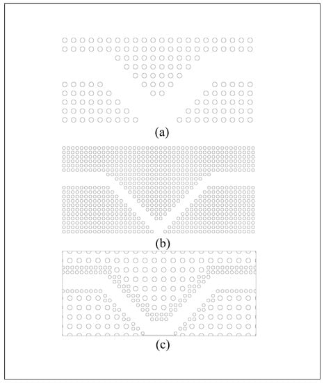
Figure 2.
(a) The PhC structure with r and d specifications larger than that of structure (b) is used to fill space, achieve better confinement, and due to its dimensions, has a more simple manufacturing process. (b) The PhC structure with r and d specifications smaller than that of structure (a) is used for better wave propagation and for adjusting the incident angle of the wave with the electronic section. (c) The hybrid structure of (a,b) is used in the optical section of ERMs.
The electronic section of the ERMs is structured as a p-i-n diode with an intrinsic region of MQWs. There are two methods for using the gold layer in this structure, as shown in Figure 3. In the first design, the gold layer is located at the interface between the optical and electronic sections of the device. In this case, the wave hitting the gold surface is considered for using hybrid plasmonic MQWs modes in the “off” state of the modulator (Figure 3a), and TM polarization is used for the incident light []. In the second design, the gold layer is located at the bottom of the p-i-n diode for better reflectance, and the optimized thickness of the gold layer is 50 nm. In this case, TE polarization is propagated []. Because TE polarization is used in the PhCs, the second design is used and investigated here.
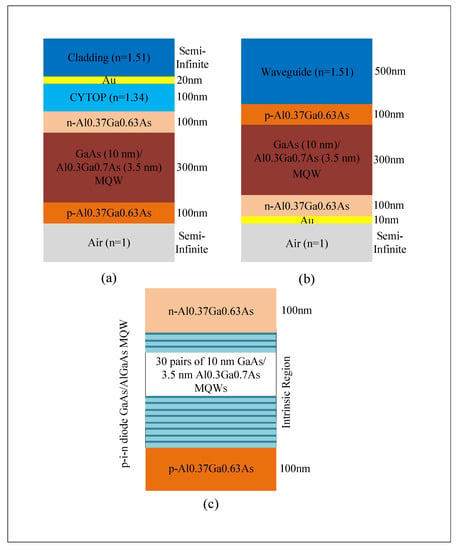
Figure 3.
(a) The gold layer is at the interface between the optical and electronic sections. TM polarization has been exploited for MQW plasmonic hybrid modes. (b) The gold layer is used at the bottom of p-i-n diode for better reflectance. In this case, TE polarization has been applied. (c) The structure of p-i-n diode is suitable and acceptable in both cases.
Previously, the electronic component has been investigated with the noted first structure p-i-n diode via performance under TM polarization []. Furthermore, the second structure has been investigated in the wavelength range of 830–870 nm [].
When 0 volts are applied to this diode, the modulator is on. Thus, the diode is off and has no special function to absorb the incident light in the PhCs layer. When a 1-volt reverse bias (or reverse bias larger than 1 volt) is applied to this diode, the modulator is off. Thus, the light is absorbed by the electronic section of the device and not transmitted to the PhCs output waveguide. The light waves are routed through the stack waveguide in the p-i-n, which causes increased damping in the “off” state of this ERMs. This is in accordance with the QCSE in MQWs of the intrinsic region. The structure of these MQWs consists of 30 pairs of 10 nm coupled layers of GaAs and 3.5 nm AlGaAs (Figure 3a).
Figure 4a shows the three-dimensional structure of the modulator, including the PhC waveguide and the p-i-n modulator. The configuration of the hybrid nanorods is shown in Figure 2c, where the light wave is confined along the rod direction. The 2D PhC rods/slab waveguides are placed perpendicular to the modulator, which is generally formed vertically on the substrate, and the input port is located on the modulator surface.
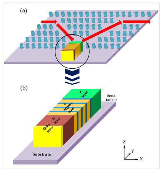
Figure 4.
(a) Three-dimensional structure of the modulator including PhC waveguide and p-i-n modulator. (b) The structure and arrangement of the electronic part of the modulator horizontally.
To address this issue, we propose a novel design in this paper which involves horizontally locating and fabricating the electronic section on the substrate surface. The p-i-n modulator is horizontally formed on the substrate for this purpose, and the input port is placed on its surface. The structure and arrangement of the electronic part of the modulator are shown in Figure 4b. This design can be fabricated using nano-fabrication processes such as patterning, deposition, developing, exposing, etching, and deletion. The design is used for the p-i-n modulator via the f–b cavity mechanism.
The proposed schematic of the coupled MQWs fabrication process is shown in Figure 5. In the first step, a substrate is provided for the growth of the designed layers. The substrate is common to the electronic and optical sections of the modulator, on which the PhCs are also implemented (Figure 5a). Next, a GaAs layer is grown to size in the intrinsic region of the p-i-n diode for deposition and patterning of the coupled MQWs (Figure 5b). The GaAs MQWs are then formed and developed through a mask and pattern process in the previous step to maintain the GaAs MQWs and vacant MQWs. The vacant MQWs are created through an etching process (Figure 5c). Finally, AlGaAs layers are deposited in the vacant MQWs (Figure 5d). Thus, an intrinsic region is created for the p-i-n diode via the coupled MQWs.
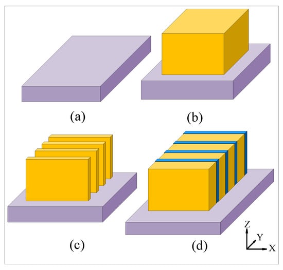
Figure 5.
Proposed schematic of coupled MQW fabrication process. (a) The substrate is provided for the growth of the designed layers (substrate is common to electronic section and the optical section of the modulator on which the PhCs is also implemented). (b) GaAs layer is grown to size in the intrinsic region of the p-i-n diode for deposition and patterning of coupled MQWs. (c) GaAs MQWs are formed and developed by mask and pattern process of the previous step to maintain the GaAs MQWs and vacant MQWs. Vacant MQWs are created by etching process. (d) AlGaAs layers are deposited in vacant MQWs. Therefore, an intrinsic is region created for the p-i-n diode via coupled MQWs.
In comparison with the usual vertically formed p-i-n modulator on the substrate, this proposed process has fewer steps of deposition. The intrinsic region of the p-i-n modulator is fabricated through masking once, etching once, and deposition once, unlike the deposition process for the usual p-i-n modulator, which repeats approximately 60 times. However, the proposed process has a big limitation, that is, the size of the masking pattern, which os 5–10 nm for the noted model. Therefore, there is a trade-off.
3. The Design of Electro-Reflective Photonic Crystals Modulators
The PhC structure with optimized materials and dimensions is utilized to design the waveguide structure and determine the angle for the incident light of the p-i-n diode. Its optimized measures are GaAs with R = 80 nm and D = 300 nm (R is the radius of the nanorods and D is the lattice constant of the PhC structure), in this state, the removed areas of the nanorods are clear. A smaller and denser gold PhC structure was utilized to fill the margins of the removed areas. Its optimized measures are R = 50 nm and D = 150 nm. Then, the removed waveguide areas and the angle of incident light is = 45° for the “on” and “off” states of the modulator. Furthermore, the dimensions of this device are 5 μm by 2.7 μm in the deflection area and the thickness of waveguide area is about 450 nm (Figure 6a).
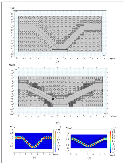
Figure 6.
(a,b) The optical sections of ERMs based on hybrid PhC structures are shown with deflection angles of 45 and 60 degrees. (c) The electric field propagation plot for TE polarization in the PhC waveguide section corresponding to part (a). (d) The electric field propagation plot for TE polarization in the PhC waveguide section corresponding to part (b).
Different angles can be created to prove that in this PhC structure, the waveguide structure and diverse angles are designed and shaped for the incident light on the p-i-n diode. For example, when investigating the incident light angle = 60°, GaAs PhC Structural specifications are optimized and calculated for R = 80 nm and D = 300 nm. In this state, the removed areas of the nanorods for the waveguiding area are visible. Smaller and denser gold PhC structures were utilized to fill the margins of the removed areas. Its optimized measures are R = 30 nm and D = 80 nm; then, the removed waveguide areas and the shape of incident light angle = 60° for the “on” and “off” states of the modulator. Furthermore, the dimensions of this device are 5.5 μm by 2.4 μm in deflection area. The thickness of the waveguide area is about 500 nm (Figure 6b). The polymer waveguide region with a refractive index of n = 1.51 was determined according to the p-i-n diode features in both structures.
The electric field propagation plot of TE polarization is shown in Figure 6c for a PhC waveguide layer with a deflection angle of 45° at 903 nm. It is analytically simulated using the finite element method. Furthermore, the electric field propagation plot of TE polarization is shown in Figure 6d for a photonic crystal waveguide layer with a deflection angle of 60° at 903 nm. At this wavelength, when the modulator is on, the transmittance is at its highest value, and the losses (or scattering) are at their lowest value.
The second structure of the p-i-n diode mentioned above is designed for the electronic section of the device, as shown in Figure 7. In this configuration, the ‘p’ region is located at the interface with the polymer waveguide, which has a refractive index of n = 1.51, and the ‘n’ region is located at the interface with the gold layer, which is located at the bottom of the structure.
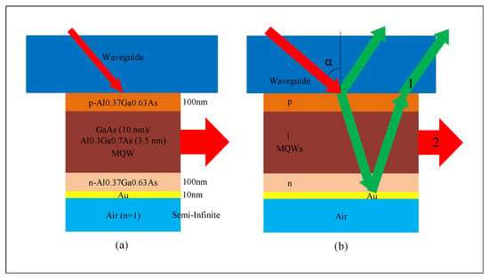
Figure 7.
(a) The structure of the electronic section for the use of TE polarization. (b) The electronic section of a PhC-based ERM into which incoming light enters at an alpha angle and undergoes two possible events: (1) green arrows denote reflected light from the electronic section to the waveguide region, or (2) a red arrow in the intrinsic region of the p-i-n diode denotes absorbed light.
The polymer coating (i.e., the waveguide region in the PhCs) and the lower gold reflector form a Fabry–Pérot cavity to increase the insertion loss (IL) in the coupled MQWs for the modulator’s “off” state, thereby increasing the extinction ratio (ER). This function is greatly improved at low voltage []. The input light is TE polarized, and it enters the electronic section of the device at an alpha angle from the polymer waveguide. It then enters the ‘p’ region and, after passing through the ‘i’ and ‘n’ regions, strikes the surface of the gold layer.
Depending on the alpha angle and the voltage applied to the diode (either zero or two volts), which is indicated by a green arrow, the light is reflected and exits the electronic section and is then coupled into the output path of the PhC waveguide (Figure 7b). Otherwise, as shown by a red arrow in the intrinsic region, the wave is propagated through the intrinsic region of the p-i-n diode, which consists of coupled MQWs and does not reach the output of the PhCs waveguide (Figure 7b).
4. Results and Discussion
A figure of merit (FOM) can be introduced when multiple parameters are used in optimization. Here, optimization is performed using parameters such as r1 (radius of large nanorods), d1 (distance between two large nanorods), r2 (radius of small nanorods), d2 (distance between two small nanorods), number of nanorods, thickness of the gold layer, and spectral data via the Nelder–Mead method simultaneously.
The utilized gold nanorods were selected from silver(Ag), aluminum (Al), and gold (Au) nanorods for small nanorods with PhCs structure, that have better characteristics for waveguide and transmission. Moreover, GaAs nanorods have been opted among GaAs, lithium niobate (LiNbO3), gallium nitrate (GaN) and gallium phosphate (GaP) for the large nanorods since GaAs nanorods have better performance.
The transmission diagrams in terms of the wavelength of the light propagated are given for the PhCs structure in the optical section of ERMs in the “on” state of the device. Transmittance curves in the PhCs are shown according to the material in the PhCs structure of large and small nanorods. The thickness of the gold layer is also considered for the reflection situation of the device in the “on” state.
In all plots, green curves correspond to a transmittance rate with a reflective gold thickness of 20 nm, and red curves correspond to the transmittance rate through a reflective gold layer with a thickness of 10 nm (Figure 8 and Figure 9).
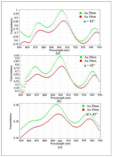
Figure 8.
(a) The transmittance diagram for the PhC structure consisting of large GaAs nanorods and small Au nanorods with a deflection angle of 45°. (b) The transmittance diagram for the PhC structure consisting of large GaAs nanorods and small Ag nanorods with a deflection angle of 45°. (c) The transmittance diagram for the PhC structure consisting of large GaAs nanorods and small Al nanorods with a deflection angle of 45°.
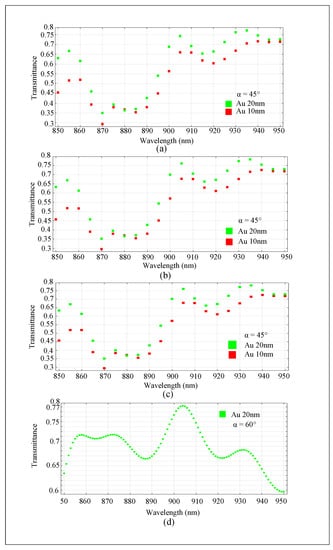
Figure 9.
(a,b) The transmittance diagram for the PhC structure consisting of large nanorods of GaP and GaN and small nanorods of Au with a deflection angle of 45°. (c) The transmittance diagram for PhC structure consisting of large LiNbO3 nanorods and small Al nanorods with a deflection angle of 45°. (d) The transmittance diagram for the PhC structure consisting of large GaAs nanorods and small Al nanorods with a deflection angle of 60°.
As can be seen, the 20 nm thickness of gold has a better reflectance than the 10 nm thickness of gold (Figure 8 and Figure 9). In fact, the 20 nm gold layer has better reflectance, and thus less light wave is leaked in the electronic section for the modulator “on” state. Therefore, it causes better transmittance for the optical section. Light is applied to the gold layer at an angle of 45°, as shown in Figure 6a.
In this analysis, we used large GaAs nanorods and small Au nanorods. The transmittance efficiency at 903 nm is 98%, and the bandwidth is in the range of 890–913 nm (23 nm) with over 80% output (Figure 8a). This special design has optimized R and D parameters, a high-contrast refractive index between the nanorods and gap, and the width of the waveguiding region is intended for these accurate and explicit wavelengths.
Additionally, we used large GaAs nanorods and small Ag nanorods. In this case, the transmittance efficiency at 898 nm is 97%, and the bandwidth is in the range of 890–907 nm (17 nm) with over 75% of the input light wave of the waveguide passed from the output waveguide by the PhC structure (Figure 8b). The transmittance values are approximately equal when the small nanorods are Au or Ag. This is because both metals have similar and nearly identical features. However, Au nanorods were chosen for this role in the device because it has a broader pass bandwidth compared to Ag.
For the next analysis, we used large GaAs nanorods and small Al nanorods. However, the transmittance efficiency at 895 nm is only 37%, which is not acceptable (Figure 8c).
In further analysis, large nanorods of GaP and GaN and small nanorods of Au are utilized in the PhCs. However, the light wave transmittance in the range of 850–950 nm is less than 77%, which is not appropriate (Figure 9a,b). In the next case, large nanorods of LiNbO3 and small nanorods of Au are consiered, but the light wave transmittance in the range of 850–950 nm is also less than 77%, which is not admissible in comparison to the GaAs and Au hybrid (Figure 9c).
In the last case, light is applied on the gold layer at an angle of 60°, as shown in Figure 4a. Large nanorods of GaAs and small nanorods of Au are devised. The transmittance efficiency in the range of 895–915 nm is between 70% and 77%, which demonstrates that changing the deflection angle from 45° to 60° has reduced the light wave transmittance (Figure 9d). This indicates that a greater deflection angle results in reduced transmittance and increased losses, which occur on the surface of the reflector layer and depend on the critical angle and angle of refraction. These parameters depend on the boundary between the gold and polymer layer, where the refractive index of the polymer layer is assumed to be 1.51.
Figure 10a–c illustrate the 3D design of a single-mode waveguide coupling with surface-incident devices via the depicted free-form reflectors. Figure 10d demonstrates the FEM simulation results for this kind of design. A pair of parabolic reflectors are used to collimate the output from a single-mode waveguide with a 40° incident angle with respect to the device and refocus the beam reflected from the surface-incident an MQW modulator back to the waveguide. The simulation reveals high coupling efficiency values of 94% (IL ∼ 0.27 dB) at 850 nm wavelength for TE polarized inputs []. The dimensions of this 3D and bulky structure for the free-form region are about 60 μm × 20 μm × 10 μm [,].
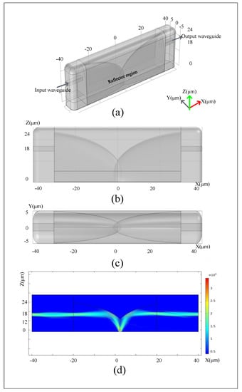
Figure 10.
(a) 3D structure of Optical Free-Form Couplers for MQWs ERMs with a pair of parabolic reflectors. (b) Side view of this scheme. (c) Top view of this scheme. (d) Side view of FEM simulation of the coupling between the polymer waveguides and the MQW modulator region are demonstrated [].
The alternative design described in this paper for the optical part of MQW ERMs (as shown in Figure 11 and Figure 12) is significantly reduced in size compared to the previous design (as shown in Figure 10), whereas this 2D PhC structure is composed of large and small hybrid PhCs with a plate size of about 3 μm × 3 μm in the area of light deflection. It has the same function while reducing the dimensions, and the coupling efficiency is still more than 90% at the noted wavelengths for MQW ERMs.

Figure 11.
(a) The PhC structure consists of large GaAs nanorods and small Au nanorods to create a deflection angle of 41°. (b) The TE mode electric field propagated in the PhC waveguide section corresponding to part a.
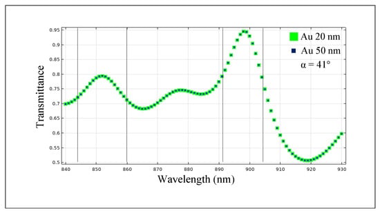
Figure 12.
The transmittance diagram for the PhCs structure consisting of large GaAs nanorods and small Au nanorods with a deflection angle of 41°.
The p-i-n diode is designed to create the ERMs in the electronic part of this device, with the intrinsic regions of this diode being coupled MQW layers of AlGaAs/GaAs. The upper polymer coating (i.e., the waveguide region in PhCs, in this context) and the lower gold reflector form a Fabry–Pérot cavity to increase the IL in the coupled MQWs, thereby greatly improving the ER at low voltage. The specifications of this electronic section of the device have been obtained as ER ∼ 6 dB and IL < 3 dB at 2 volts for the incident light angles of 38° and 41°. A more optimized modulator design can reach a peak ER of about 9–12 dB at 2 volts with a low IL of about 2–3 dB and a relatively wide spectral bandwidth of about 10 nm. It has also achieved low IL and high ER values for wavelengths of 856 nm. This device has better characteristics than similar devices [].
Here, the same specifications are intended for the electronic part of the modulator, and thus the angle of incident light in the optical part can be adjusted to 38° and 41° accordingly. This novel scheme is designed for the 41° angle of the optical section using integrated PhCs (Figure 11a). The electric field propagation in the waveguide path of this PhCs for a wavelength of 896 nm is shown in Figure 11b.
As shown by the PhC design in Figure 11, significant light confinement and no light scattering occurs in specific regions. The electronic part of the modulator operates at a frequency of 856 nm, with light wave transmittances of 70–80% in the frequency range of 846–860 nm, and a maximum of 80% at 852 nm in the modulator’s “on” state.
However, due to the optimized R, D, and waveguiding region width parameters of this special design, if the operating frequency is in the range close to 900 nm, the light wave transmittance is more than 80% in the range of 891–904 nm, with a peak of 95% at a wavelength of 897 nm, as shown in Figure 12. The transmittance in the “on” state is sufficiently desirable, and the incident light angle can be adjusted to the electronic section of the device.
Furthermore, the optical part of the modulator has a significantly reduced size in comparison to three-dimensional models [], and the two-dimensional PhC design enables a simpler fabrication process, making it advantageous for integration with optical integrated circuits (OICs) and connection with other components in photonic integrated circuits (PICs), both optical and optoelectronic.
The PhC structure is composed of large GaAs nanorods and small Au nanorods to achieve a deflection angle of 37° for the modulator “on” state at zero-volt bias, as shown in Figure 13a. In this case, the TE mode is propagated in the modulator, as depicted in Figure 13b. The electronic part of the device is also designed and optimized based on the release of TE mode for both “on” and “off” states of the modulator. For this simulation, the effective refractive index of the intrinsic region of the p-i-n diode consisting of coupled MQWs is considered to be , and for the “off” state of the modulator, which corresponds to a 2-volt bias applied to the diode, cm). Additionally, the thickness of the gold layer is 50 nm [].
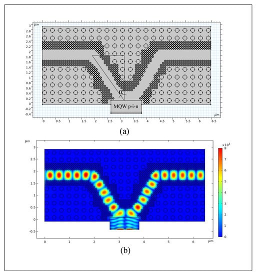
Figure 13.
(a) The PhC structure elements to create a deflection angle of 37° at zero-volt bias (the modulator is on). (b) The electric field of TE polarization emitted in the PhCs waveguide corresponding to section a.
In Figure 13, it can be noted that when the modulator is turned on, the light wave transmittance is more than 80% at the 867–875 nm range for the PhC structure. This is due to the special design with optimized R and D parameters, a high-contrast refractive index between the nanorods and gap, and awaveguiding region width selected for these specific wavelengths. The parameters of the Fabry–Pérot cavity, located between the polymer coating and p-i-n diode, also have an effect on the transmittance value of the light wave in this situation. Furthermore, designing the structure with a Fabry–Pérot cavity has reduced the range of the light wave transmittance bandwidth, as shown in Figure 14.
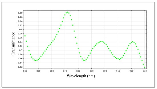
Figure 14.
The transmittance diagram corresponding to Figure 13a,b.
Taking into account the limitations and conditions of current fabrication technology, the proposed structure was designed and simulated with random tolerance of Au and GaAs nanorod radii. This approach makes the results of the simulation and proposed design closer to the reality of the experimental sample.
As shown in Figure 15a, a tolerance between 77.5 nm and 82.5 nm, with a step of 0.5 nm, was assumed for random changes in GaAs nanorod radius. Similarly, a range of 47.5 nm to 52.5 nm, with a step of 0.5 nm, was randomly used for the gold nanorod radius. These changes were applied to the structure in the worst-case scenario, where all GaAs and Au nanorods have some tolerances due to errors in the fabrication technology. The number of nanorods that undergo these changes was applied randomly within the range stated in the design. The average radius of GaAs and Au nanorods was then calculated. This process was repeated 100 times, and the transmission rate was calculated each time. The transmission rate for different states is shown in the diagram of Figure 15b. This diagram depicts the transmittance in terms of the average radius of GaAs and Au nanorods. According to this graph, at least half of the states considered with tolerance still have a transmittance of more than 80%. Therefore, the probabilistic fabrication limitations and faults are taken into account in the proposed novel structure via random and presumptive parameters in simulation.
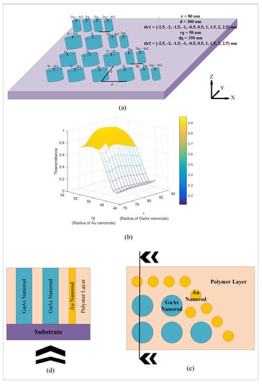
Figure 15.
(a) Design and schematic of the proposed structure with radius random tolerance of Au and GaAs nanorods performed simultaneously. (b) The transmittance in terms of the average radius of GaAs and Au nanorods is depicted simultaneously. (c) A part of the proposed structure consisting of polymer layer and GaAs and Au nanorods. (d) Schematic of the polymer layer and GaAs and Au nanorods placed together vertically.
Figure 15c shows a schematic of a part of the proposed structure, consisting of a polymer layer, GaAs, and Au nanorods. The wave propagation occurs in the polymer layer and the specific gap between the PhC structure. In Figure 15d, a section of the previous schematic is shown, which demonstrates how the polymer layer and GaAs and Au nanorods are vertically placed together. The process model and fabrication technology of this new structure have been put forward through these schematics.
5. Conclusions
The adaptability and compatibility of coupling different elements to each other is very momentous for the realization of integrated connection in the PICs and OICs. Accordingly, lower dimensions and lower losses are always considered of high importance and are thus developed. In this paper, an electro-reflective modulator was investigated, which consists of an optical section (PhCs) and an electronic section (including a p-i-n diode with an intrinsic region of coupled MQWs).
A novel design of these modulators was executed in its optical region using the integrated PhC structure. This two-dimensional structure greatly reduces the dimensions of optical section and has more cost-effective fabrication processes than the bulky 3D components. The transmittance and bandwidth have increased, because this design is optimized for the lowest amount of losses, and the scattering of light in the waveguide and deflection route is low. It justifies the utilization of PhC structure in the optical part of the ERMs. Simultaneously, changing the deflection angle to create the desired angle of incident light to the electronic part of the device simplifies the design of the electronic part of the device. The PhC structure in the optical section of this device resulted in better linkage and excellent compatibility with other optical elements in the PICs.
OICs can utilize this structure in other optical elements such as functional modulators, optical switches, optical waveguides with bends, optical logic gates, optical computational circuits, and optical filters.
Author Contributions
Conceptualization, M.M.K.H. and F.E.; methodology, M.M.K.H. and F.E.; software, M.M.K.H. and F.E.; data curation, M.M.K.H. and F.E.; validation, M.M.K.H. and F.E.; formal analysis, M.M.K.H. and F.E.; investigation, M.M.K.H. and F.E.; resources, M.M.K.H.; writing—original draft preparation, M.M.K.H.; writing—review and editing, M.M.K.H. and F.E.; visualization, M.M.K.H. and F.E.; supervision, F.E.; project administration, F.E. All authors have read and agreed to the published version of the manuscript.
Funding
This research received no external funding.
Data Availability Statement
Data underlying the results presented in this paper are not publicly available at this time but may be obtained from the corresponding author upon reasonable request.
Conflicts of Interest
The authors declare no conflict of interest.
References
- Wang, X.; Liu, J. Emerging technologies in Si active photonics. J. Semicond. 2018, 39, 061001. [Google Scholar] [CrossRef]
- Shen, Y.; Meng, X.; Cheng, Q.; Rumley, S.; Abrams, N.; Gazman, A.; Manzhosov, E.; Glick, M.S.; Bergman, K. Silicon photonics for extreme scale systems. J. Light. Technol. 2019, 37, 245–259. [Google Scholar]
- Yu, S.; Zuo, H.; Wang, X.; Sun, X.; Liu, J.; Hu, J.; Gu, T. Seamless hybrid-integrated interconnect network (SHINE). In Proceedings of the 2019 Optical Fiber Communications Conference and Exhibition (OFC), San Diego, CA, USA, 3–7 March 2019; IEEE: Piscataway, NJ, USA, 2019; pp. 1–3. [Google Scholar]
- Yu, S.; Zuo, H.; Sun, X.; Liu, J.; Gu, T.; Hu, J. Optical Free-form couplers for high-density integrated photonics (OFFCHIP): A universal optical interface. J. Light. Technol. 2020, 38, 3358–3365. [Google Scholar] [CrossRef]
- Han, S.P.; Kim, J.T.; Jung, S.W.; Ahn, S.H.; Choi, C.G.; Jeong, M.Y. A reflective curved mirror with low coupling loss for optical interconnection. IEEE Photonics Technol. Lett. 2004, 16, 185–187. [Google Scholar] [CrossRef]
- Dangel, R.; Hofrichter, J.; Horst, F.; Jubin, D.; La Porta, A.; Meier, N.; Soganci, I.M.; Weiss, J.; Offrein, B.J. Polymer waveguides for electro-optical integration in data centers and high-performance computers. Opt. Express 2015, 23, 4736–4750. [Google Scholar] [CrossRef] [PubMed]
- Mikawa, T.; Kinoshita, M.; Hiruma, K.; Ishitsuka, T.; Okabe, M.; Hiramatsu, S.; Furuyama, H.; Matsui, T.; Kumai, K.; Ibaragi, O.; et al. Implementation of active interposer for high-speed and low-cost chip level optical interconnects. IEEE J. Sel. Top. Quantum Electron. 2003, 9, 452–459. [Google Scholar]
- Li, L.; Zou, Y.; Lin, H.; Hu, J.; Sun, X.; Feng, N.N.; Danto, S.; Richardson, K.; Gu, T.; Haney, M. A fully-integrated flexible photonic platform for chip-to-chip optical interconnects. J. Light. Technol. 2013, 31, 4080–4086. [Google Scholar] [CrossRef]
- Nieweglowski, K.; Lorenz, L.; Lüngen, S.; Tiedje, T.; Wolter, K.J.; Bock, K. Optical coupling with flexible polymer waveguides for chip-to-chip interconnects in electronic systems. Microelectron. Reliab. 2018, 84, 121–126. [Google Scholar]
- Barwicz, T.; Taira, Y.; Lichoulas, T.W.; Boyer, N.; Martin, Y.; Numata, H.; Nah, J.W.; Takenobu, S.; Janta-Polczynski, A.; Kimbrell, E.L.; et al. A novel approach to photonic packaging leveraging existing high-throughput microelectronic facilities. IEEE J. Sel. Top. Quantum Electron. 2016, 22, 455–466. [Google Scholar] [CrossRef]
- Hu, J.; Li, L.; Lin, H.; Zhang, P.; Zhou, W.; Ma, Z. Flexible integrated photonics: Where materials, mechanics and optics meet. Opt. Mater. Express 2013, 3, 1313–1331. [Google Scholar]
- Hiramatsu, S.; Mikawa, T. Optical design of active interposer for high-speed chip level optical interconnects. J. Light. Technol. 2006, 24, 927. [Google Scholar] [CrossRef]
- Cho, I.K.; Lee, W.J.; Rho, B.S.; Jeong, M.Y. Polymer waveguide with integrated reflector mirrors for an inter-chip link system. Opt. Commun. 2008, 281, 4906–4909. [Google Scholar] [CrossRef]
- Ogunsola, O.; Thacker, H.; Bachim, B.; Bakir, M.; Pikarsky, J.; Gaylord, T.K.; Meindl, J. Chip-level waveguide-mirror-pillar optical interconnect structure. IEEE Photonics Technol. Lett. 2006, 18, 1672–1674. [Google Scholar] [CrossRef]
- Lin, X.; Hosseini, A.; Dou, X.; Subbaraman, H.; Chen, R.T. Low-cost board-to-board optical interconnects using molded polymer waveguide with 45 degree mirrors and inkjet-printed micro-lenses as proximity vertical coupler. Opt. Express 2013, 21, 60–69. [Google Scholar] [CrossRef] [PubMed]
- Li, G.; Yao, J.; Thacker, H.; Mekis, A.; Zheng, X.; Shubin, I.; Luo, Y.; Lee, J.H.; Raj, K.; Cunningham, J.E.; et al. Ultralow-loss, high-density SOI optical waveguide routing for macrochip interconnects. Opt. Express 2012, 20, 12035–12039. [Google Scholar] [CrossRef] [PubMed]
- Geng, Q.; Wang, D.; Chen, P.; Chen, S.C. Ultrafast multi-focus 3-D nano-fabrication based on two-photon polymerization. Nat. Commun. 2019, 10, 2179. [Google Scholar] [CrossRef]
- Saha, S.K.; Wang, D.; Nguyen, V.H.; Chang, Y.; Oakdale, J.S.; Chen, S.C. Scalable submicrometer additive manufacturing. Science 2019, 366, 105–109. [Google Scholar] [CrossRef]
- Faraji Rad, Z.; Prewett, P.D.; Davies, G.J. High-resolution two-photon polymerization: The most versatile technique for the fabrication of microneedle arrays. Microsyst. Nanoeng. 2021, 7, 71. [Google Scholar] [CrossRef]
- Borisov, R.; Dorojkina, G.; Koroteev, N.; Kozenkov, V.; Magnitskii, S.; Malakhov, D.; Tarasishin, A.; Zheltikov, A. Fabrication of three-dimensional periodic microstructures by means of two-photon polymerization. Appl. Phys. B Lasers Opt. 1998, 67, 765. [Google Scholar] [CrossRef]
- Serbin, J.; Egbert, A.; Ostendorf, A.; Chichkov, B.; Houbertz, R.; Domann, G.; Schulz, J.; Cronauer, C.; Fröhlich, L.; Popall, M. Femtosecond laser-induced two-photon polymerization of inorganic–organic hybrid materials for applications in photonics. Opt. Lett. 2003, 28, 301–303. [Google Scholar] [CrossRef]
- Serbin, J.; Ovsianikov, A.; Chichkov, B. Fabrication of woodpile structures by two-photon polymerization and investigation of their optical properties. Opt. Express 2004, 12, 5221–5228. [Google Scholar] [CrossRef] [PubMed]
- Liu, Y.; Wang, H.; Ho, J.; Ng, R.C.; Ng, R.J.; Hall-Chen, V.H.; Koay, E.H.; Dong, Z.; Liu, H.; Qiu, C.W.; et al. Structural color three-dimensional printing by shrinking photonic crystals. Nat. Commun. 2019, 10, 4340. [Google Scholar] [CrossRef] [PubMed]
- Lindenmann, N.; Balthasar, G.; Hillerkuss, D.; Schmogrow, R.; Jordan, M.; Leuthold, J.; Freude, W.; Koos, C. Photonic wire bonding: A novel concept for chip-scale interconnects. Opt. Express 2012, 20, 17667–17677. [Google Scholar] [CrossRef] [PubMed]
- Billah, M.R.; Blaicher, M.; Hoose, T.; Dietrich, P.I.; Marin-Palomo, P.; Lindenmann, N.; Nesic, A.; Hofmann, A.; Troppenz, U.; Moehrle, M.; et al. Hybrid integration of silicon photonics circuits and InP lasers by photonic wire bonding. Optica 2018, 5, 876–883. [Google Scholar] [CrossRef]
- Lindenmann, N.; Dottermusch, S.; Goedecke, M.L.; Hoose, T.; Billah, M.R.; Onanuga, T.P.; Hofmann, A.; Freude, W.; Koos, C. Connecting silicon photonic circuits to multicore fibers by photonic wire bonding. J. Light. Technol. 2014, 33, 755–760. [Google Scholar] [CrossRef]
- Gissibl, T.; Thiele, S.; Herkommer, A.; Giessen, H. Two-photon direct laser writing of ultracompact multi-lens objectives. Nat. Photonics 2016, 10, 554–560. [Google Scholar] [CrossRef]
- Toulouse, A.; Thiele, S.; Giessen, H.; Herkommer, A.M. Alignment-free integration of apertures and nontransparent hulls into 3D-printed micro-optics. Opt. Lett. 2018, 43, 5283–5286. [Google Scholar] [CrossRef]
- Gissibl, T.; Thiele, S.; Herkommer, A.; Giessen, H. Sub-micrometre accurate free-form optics by three-dimensional printing on single-mode fibres. Nat. Commun. 2016, 7, 11763. [Google Scholar] [CrossRef]
- Dietrich, P.I.; Blaicher, M.; Reuter, I.; Billah, M.; Hoose, T.; Hofmann, A.; Caer, C.; Dangel, R.; Offrein, B.; Troppenz, U.; et al. In situ 3D nanoprinting of free-form coupling elements for hybrid photonic integration. Nat. Photonics 2018, 12, 241–247. [Google Scholar] [CrossRef]
- Gordillo, O.A.J.; Chaitanya, S.; Chang, Y.C.; Dave, U.D.; Mohanty, A.; Lipson, M. Plug-and-play fiber to waveguide connector. Opt. Express 2019, 27, 20305–20310. [Google Scholar] [CrossRef]
- Wang, X.; Yu, S.; Zuo, H.; Sun, X.; Hu, J.; Gu, T.; Liu, J. Design of hybrid plasmonic multi-quantum-well electro-reflective modulators towards< 100 fJ/bit photonic links. IEEE J. Sel. Top. Quantum Electron. 2020, 27, 1–8. [Google Scholar]
- Wang, X.; Yu, S.; Qin, J.; Cuervo-Covian, A.; Zuo, H.; Sun, X.; Hu, J.; Gu, T.; Liu, J. Low-voltage, coupled multiple quantum well electroreflective modulators towards ultralow power inter-chip optical interconnects. J. Light. Technol. 2020, 38, 3414–3421. [Google Scholar] [CrossRef]
- Rafiee, E.; Emami, F.; Negahdari, R. Design of a novel nano plasmonic-dielectric photonic crystal power splitter suitable for photonic integrated circuits. Optik 2018, 172, 234–240. [Google Scholar] [CrossRef]
- Negahdari, R.; Rafiee, E.; Emami, F.; Pakarzadeh, H. Design of tunable ring-shaped plasmonic photonic crystal filters infiltrated with optical fluids. Opt. Eng. 2021, 60, 097102. [Google Scholar] [CrossRef]
- Askarian, A.; Akbarizadeh, G.; Fartash, M. A novel proposal for all optical half-subtractor based on photonic crystals. Opt. Quantum Electron. 2019, 51, 1–9. [Google Scholar] [CrossRef]
- Rafiee, E.; Emami, F. Realization of tunable optical channel drop filter based on photonic crystal octagonal shaped structure. Optik 2018, 171, 798–802. [Google Scholar] [CrossRef]
- Hajshahvaladi, L.; Kaatuzian, H.; Moghaddasi, M.; Danaie, M. Hybridization of surface plasmons and photonic crystal resonators for high-sensitivity and high-resolution sensing applications. Sci. Rep. 2022, 12, 21292. [Google Scholar] [CrossRef]
- Veisi, E.; Seifouri, M.; Olyaee, S. Ultra-compact and Fast All-optical Photonic Crystal Half-subtractor Logic Gate. In Proceedings of the 2022 30th International Conference on Electrical Engineering (ICEE), Tehran, Iran, 17–19 May 2022; IEEE: Piscataway, NJ, USA, 2022; pp. 869–873. [Google Scholar]
- Parandin, F.; Sheykhian, A. Design of an all-optical half adder based on photonic crystal ring resonator. Opt. Quantum Electron. 2022, 54, 443. [Google Scholar] [CrossRef]
- Moshfe, S.; Abedi, K.; Moravvej-Farshi, M.K. Fully integrated 3-bit all-optical analog to digital converter based on photonic crystal semiconductor optical amplifier. Opt. Laser Technol. 2022, 148, 107773. [Google Scholar] [CrossRef]
- Hong, Y.H.; Miao, W.C.; Hsu, W.C.; Hong, K.B.; Lin, C.L.; Lin, C.; Chen, S.C.; Kuo, H.C. Progress of photonic-crystal surface-emitting lasers: A paradigm shift in LiDAR application. Crystals 2022, 12, 800. [Google Scholar] [CrossRef]
- Reilly, K.J.; Kalapala, A.; Song, A.; Rotter, T.; Liu, Z.; Renteria, E.; Fan, S.; Zhou, W.; Balakrishnan, G. Fabrication of Photonic Crystal Surface Emitting Lasers (PCSELs) by Epitaxial Regrowth. In Proceedings of the CLEO: QELS_Fundamental Science, San Jose, CA, USA, 9–14 May 2021; Optica Publishing Group: Washington, DC, USA, 2021; p. JTu3A.78. [Google Scholar]
- Reilly, K.J.; Kalapala, A.; Yeom, S.; Addamane, S.J.; Renteria, E.; Zhou, W.; Balakrishnan, G. Epitaxial regrowth and hole shape engineering for photonic crystal surface emitting lasers (PCSELs). J. Cryst. Growth 2020, 535, 125531. [Google Scholar] [CrossRef]
- Zhou, X.; Ma, X.; Zhao, S.; Qu, H.; Qi, A.; Zheng, W. Photonic crystal diode laser arrays integrated with a phase shifter designed for narrow far-field angle. In Proceedings of the 2018 Conference on Lasers and Electro-Optics (CLEO), San Jose, CA, USA, 13–18 May 2018; IEEE: Piscataway, NJ, USA, 2018; pp. 1–2. [Google Scholar]
- Kamran, M.; Abedi, K.; Sharifi, M.J. Novel multi-stage photonic crystal Mach-Zehnder optical filters. IEEE Photonics Technol. Lett. 2018, 30, 1874–1877. [Google Scholar] [CrossRef]
- Rajasekar, R.; Raja, G.T.; Robinson, S. Numerical investigation of reconfigurable photonic crystal switch based on phase change nanomaterial. IEEE Trans. Nanotechnol. 2020, 19, 545–552. [Google Scholar] [CrossRef]
- Kazanskiy, N.L.; Butt, M.A.; Khonina, S.N. 2D-Heterostructure photonic crystal formation for on-chip polarization division multiplexing. Photonics 2021, 8, 313. [Google Scholar] [CrossRef]
- Li, M.; Ling, J.; He, Y.; Javid, U.A.; Xue, S.; Lin, Q. Lithium niobate photonic-crystal electro-optic modulator. Nat. Commun. 2020, 11, 4123. [Google Scholar] [CrossRef]
- Fathi, F.; Rashidi, M.R.; Pakchin, P.S.; Ahmadi-Kandjani, S.; Nikniazi, A. Photonic crystal based biosensors: Emerging inverse opals for biomarker detection. Talanta 2021, 221, 121615. [Google Scholar] [CrossRef]
- Shi, C.; Yuan, J.; Luo, X.; Shi, S.; Lu, S.; Yuan, P.; Xu, W.; Chen, Z.; Yu, H. Transmission characteristics of multi-structure bandgap for lithium niobate integrated photonic crystal and waveguide. Opt. Commun. 2020, 461, 125222. [Google Scholar] [CrossRef]
- Zhang, C.; Yoshimi, H.; Ota, Y.; Iwamoto, S. Two-dimensional Topological Photonic Crystals with Helical Edge States below the Light Line. In Proceedings of the 2021 26th Microoptics Conference (MOC), Hamamatsu, Japan, 26–29 September 2021; IEEE: Piscataway, NJ, USA, 2021; pp. 1–2. [Google Scholar]
- Yoshimi, H.; Yamaguchi, T.; Ota, Y.; Arakawa, Y.; Iwamoto, S. Slow light waveguides in topological valley photonic crystals. Opt. Lett. 2020, 45, 2648–2651. [Google Scholar] [CrossRef]
- Dong, G.; Yang, X.; Cai, L.; Shen, X.; Wang, Y. Improvement of transmission properties through two-bend resonance by holographic design for a two-dimemsional photonic crystal waveguide. Opt. Express 2008, 16, 15375–15381. [Google Scholar] [CrossRef]
- Iwamoto, S.; Ota, Y.; Arakawa, Y. Recent progress in topological waveguides and nanocavities in a semiconductor photonic crystal platform. Opt. Mater. Express 2021, 11, 319–337. [Google Scholar] [CrossRef]
- Tokushima, M.; Ushida, J.; Gomyo, A.; Shirane, M.; Yamada, H. Efficient transmission mechanisms for waveguides with 90 bends in pillar photonic crystals. JOSA B 2005, 22, 2472–2479. [Google Scholar] [CrossRef]
- Vishnoi, A.; Mudi, R.; Debnath, K. Systematic design study of waveguides and waveguide bends in diamond-structured photonic crystals. JOSA B 2021, 38, 907–913. [Google Scholar] [CrossRef]
- Robin, Y.; Bae, S.; Shubina, T.; Pristovsek, M.; Evropeitsev, E.; Kirilenko, D.; Davydov, V.Y.; Smirnov, A.; Toropov, A.; Jmerik, V.; et al. Insight into the performance of multi-color InGaN/GaN nanorod light emitting diodes. Sci. Rep. 2018, 8, 7311. [Google Scholar] [CrossRef] [PubMed]
- Glukhov, I.A.; Dadoenkova, Y.S.; Bentivegna, F.F.; Moiseev, S.G. Deterministic aperiodic photonic crystal with a 2D array of metallic nanoparticles as polarization-sensitive dichroic filter. J. Appl. Phys. 2020, 128, 053101. [Google Scholar] [CrossRef]
- Wang, H.C.; Martin, O.J. Polarization-Controlled Chromo-Encryption. Adv. Opt. Mater. 2023, 2202165. [Google Scholar] [CrossRef]
- Zhang, L.; Chang, S.; Chen, X.; Ding, Y.; Rahman, M.T.; Duan, Y.; Stephen, M.; Ni, X. High-Efficiency, 80 mm Aperture Metalens Telescope. Nano Lett. 2022. [Google Scholar] [CrossRef]
- Heshmati, M.M.K.; Emami, F. Numerical Investigations of 2-D Optical Free-Form Couplers for Surface Connections of Photonic Integrated Circuits. Results Opt. 2023, 10, 100351. [Google Scholar] [CrossRef]
Disclaimer/Publisher’s Note: The statements, opinions and data contained in all publications are solely those of the individual author(s) and contributor(s) and not of MDPI and/or the editor(s). MDPI and/or the editor(s) disclaim responsibility for any injury to people or property resulting from any ideas, methods, instructions or products referred to in the content. |
© 2023 by the authors. Licensee MDPI, Basel, Switzerland. This article is an open access article distributed under the terms and conditions of the Creative Commons Attribution (CC BY) license (https://creativecommons.org/licenses/by/4.0/).