Article

Coupled Plasmon Wave Dynamics beyond Anomalous Reflection: A Phase Gradient Copper Metasurface for the Visible to Near-Infrared Spectrum

1
Electrical and Computer Engineering, The University of Alabama, Tuscaloosa, AL 35487, USA
2
Remote Sensing Center, The University of Alabama, Tuscaloosa, AL 35487, USA
Optics 2022, 3(3), 243-253; https://doi.org/10.3390/opt3030024
Submission received: 2 June 2022 / Revised: 10 July 2022 / Accepted: 13 July 2022 / Published: 15 July 2022

Abstract

:
In nanoscale photonic devices, the demand for multifunctionality from 2D metasurface optics has increased rapidly. To explore the required fine-tuning in the design metrics, we reinvestigated the trapezoid-shape copper metasurface using finite-difference time-domain simulation to efficiently utilize linearly polarized light for two different functionalities. From the plasmonic band structure, we could see how the degree of asymmetry in the geometry affected the efficient resonance coupling of the traveling plasmonic modes, along with the different types of mode hybridization profiles that were related to the nanoantenna’s geometric shape. By tuning the nanoantenna’s length, we could excite the effective plasmon mode that was supported by this configuration and guide surface waves unidirectionally from the normal incidence free-space light within the visible to infrared range. The directed surface plasmon polaritons had both antisymmetric and symmetric modes that oscillated between the top and bottom surfaces of the continuous metal layer, depending on the nanoantenna’s length and wavelength. This proposed copper metasurface was optimized for a far-field application of broadband (600–900 nm) anomalous beam steering for an average of 60% efficiency with a maximum angle of 64°. This work offers more understanding of a metasurface being implemented in small plasmonic devices, waveguide mode controlling and beam steering with wavelength-dependent functionalities.

1. Introduction

The demand for subwavelength-scale engineering for compact flexible optics and the exploration of the critical limits of light–matter interaction are both proliferating. The promising applications of these optoelectronic devices in optical holography, superlens imaging, polarimetric detecting, beam steering, waveguide coupling, beam splitting and vortex beam generation have successfully replaced bulky optics [1,2,3,4]. Though remarkable results and utility have been demonstrated using optical metasurfaces for photonic devices, multifunctionality and wavelength-dependent multiplexing remain challenging [5,6]. Plasmonic metasurfaces have become more popular because of their subwavelength-scale aspect ratio and gap surface plasmon (GSP)-assisted tuning option for the better control of resonance loss. Highly efficient reflection orders can be controlled by magnetic coupling [5,7,8,9]. A metasurface with a silver trapezoid-shape nanoantenna was investigated by Li et al. within the visible wavelength range to demonstrate angle-resolved broadband beam splitting [5]. A concurrent report from Zhang et al. studied a gold trapezoid-shape metasurface [10]. Lei et al. came up with the new idea of tuning the resonance coupling between a dipole and an imperfect image of the silver trapezoid-shape antenna to achieve both anomalous reflection and transmission within the visible wavelength spectrum, but the design was challenging in terms of fabrication [7]. Gao et al. conducted excellent work on a wavelength-insensitive phase gradient aluminum trapezoid nanoantenna for propagating waves (PWs), but they did not explore the plasmonic effects [11]. The work of Sun et al. with discrete bar nanoantennae connected the phase gradient to the onset of surface waves (SWs) and the angular dependency of anomalously reflected beams [12,13]. Li et al. demonstrated the mode conversion, polarization rotation and asymmetric coupling of the waveguide modes for the mid-IR range using a metasurface with a small footprint and gradient phase gold nanoantenna for the dielectric waveguide [14]. The flat metal trapezoid nanoantenna over continuous insulator and metal layer has been reported in the literature are included in Table 1. Within the last decade, many works have reported approaches to new possibilities, yet more investigation is required into how one metasurface can be used efficiently for both PWs and SWs in a controlled manner.
In this article, we report a copper metasurface as the plasmonic material. Both gold and silver have been extensively investigated in the literature, but not as much attention has been paid to copper. The interband transition energy level for copper is 2.15 eV and has the capability of interband excitation within the visible wavelength range, compared to the 4 eV of gold [16]. The oxidation of copper is an issue, which has been improved by the use of capping agents over recent years [17,18]. Photonics devices can also be made cost-effectively using copper. Using finite-difference time-domain (FDTD) simulation (2021R1.2 FDTD Solutions, Ansys/Lumerical), we explored the design of a metasurface that was optimized for the visible to near-infrared spectrum for anomalous reflection and SPP channeling. This article is divided into two sections to discuss these two aspects of our metasurface design.

2. Simulation and Modeling

We chose for the thickness of the copper trapezoid nanoantenna to be 50 nm (λ/10 − λ/24) to overcome the skin depth of the Cu–SiO2 system with a continuous SiO2 spacer (h = 50 nm) and a 100-nm Cu bottom layer (Figure 1a) for a working wavelength range of 500–1200 nm. The value of the optical constant for the simulation and calculations was taken from the book of Palik [19]. We maintained a constant gap of 62 nm between the tip to the base and a constant base width of b = 185 nm, a tip of 20 nm and a periodicity toward the base of PW = 349 nm. We changed the length (L = 918, 825, 700 and 550 nm), as well as the corresponding periodicity PL toward the length direction (see Table S1 in the Supplementary Materials) to optimize the length of the trapezoid. Plane wave source was used for the reflection, phase profile and wavelength-dependent SPP excitation using a Bloch boundary condition in the x and y directions, with a PML toward z. For the scattering and absorption cross-sections, power flows and SPP wave propagation, a total-field/scattered-field (TFSF) source was used from the top of all of the PML boundaries. For the band structure calculations, modes were excited using a randomly oriented electric dipole near the Cu nanoantenna–SiO2 interface and the results were obtained from up to the first Brillouin zone edge. In this article, our interest was mainly in 918-nm and 550-nm trapezoids, which we will refer to as 918L and 550L, respectively.

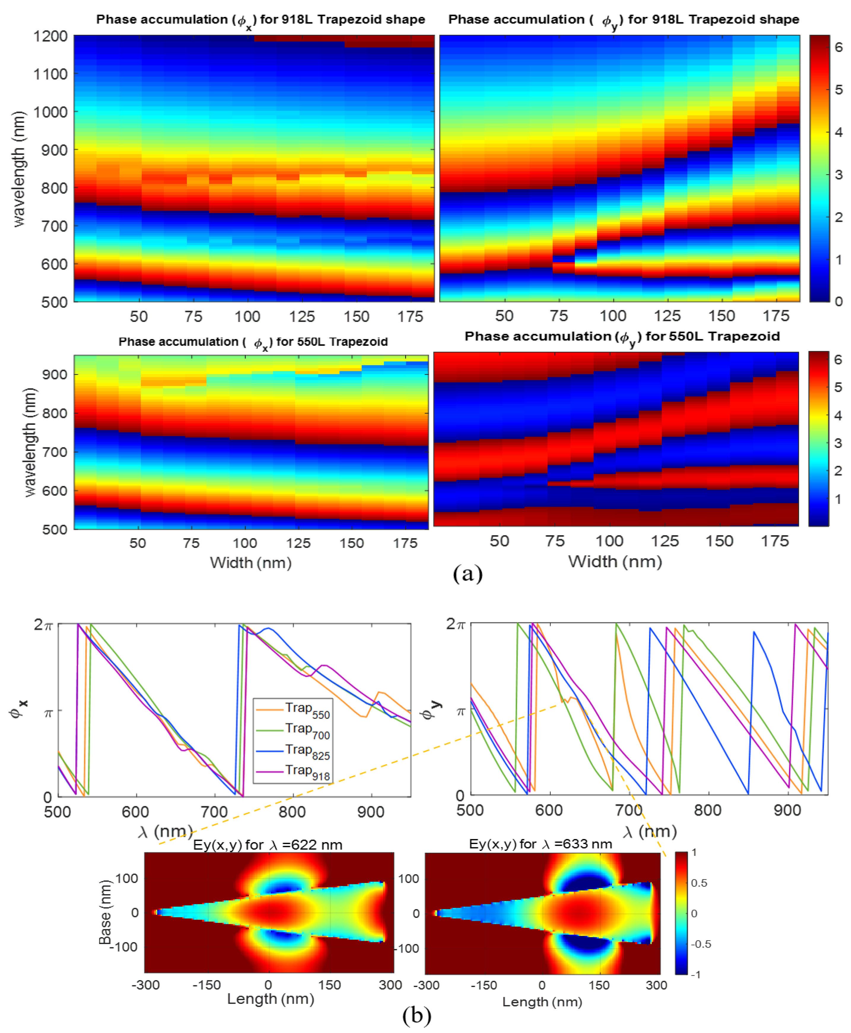
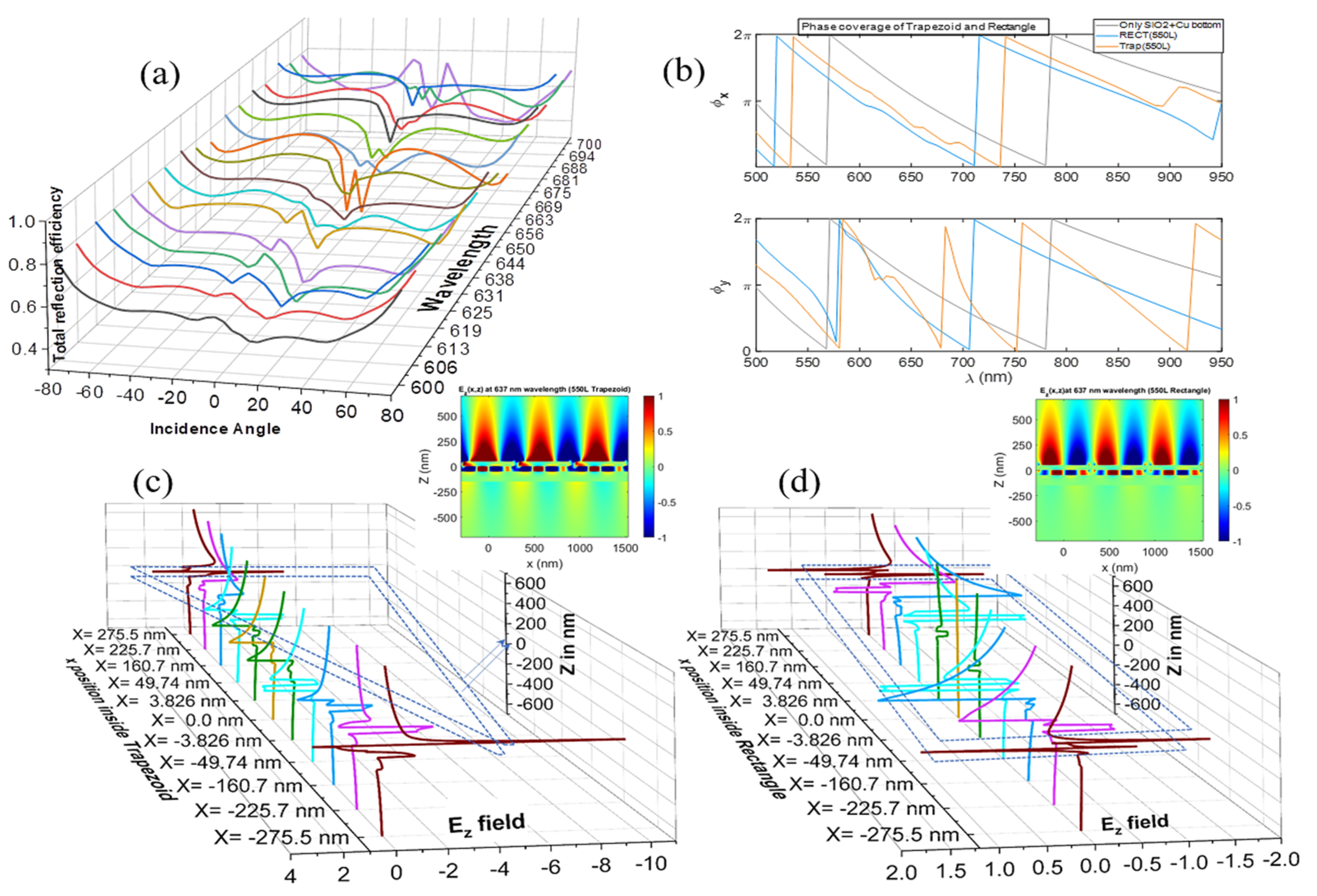
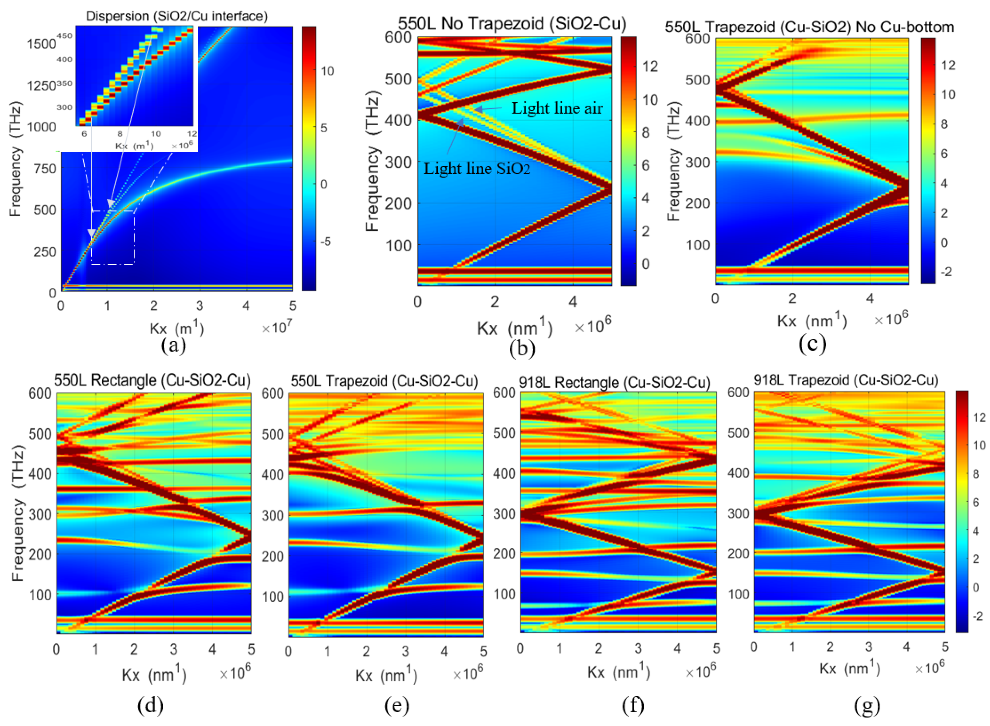
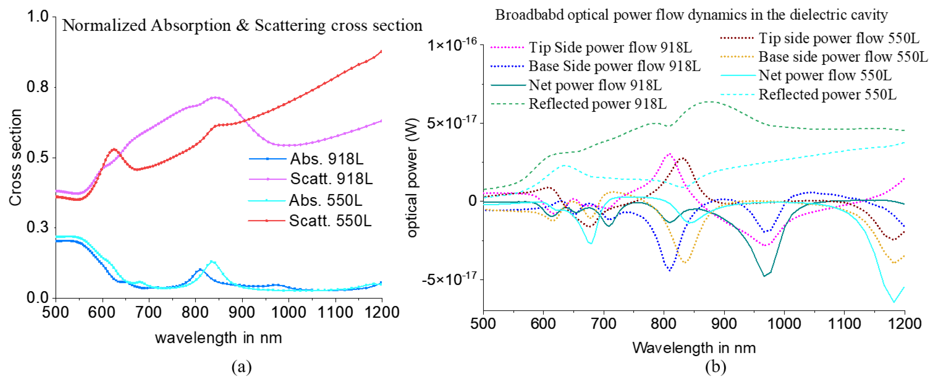
3. Results and Discussion

The phase shift that was offered by the trapezoid nanoantenna, which was symmetric under normal incidence y-polarized light, varied linearly along the x direction, which conveyed with dφ(x)/dx in the generalized form of Snell’s law:
n r , t   sin θ r , t n i   sin θ i = m 0 λ 0 P x + λ 0 2 π   d Φ ( x ) dx
where nr,t, and ni are the refractive indices of the reflected and transmitted medium, respectively. The subscript m signifies the diffraction order. Equation (1) is a simple grating equation with a maximum accumulation of the additional phase 2π within one periodicity of a unit cell. the term produced dφ(x)/dx = 2π/Px.
n r , t   sin θ r , t n i   sin θ i = ( m 0 + 1 ) λ 0   P x
So, the prominent order of the power flows shifted to a positive first-order diffraction after the reflection or transmission [5,7,20]. For wider angle and higher efficiency anomalous reflection (AR) in the 500–950 nm broadband range, we obtained the optimal aspect ratio and length of the trapezoid, as shown in Figure 1b,e,f and Figure S1.1b. Below a 550-nm wavelength, the reflection efficiency of the plain SiO2–Cu surface was low, so copper was not a good candidate; however, above that wavelength, the efficiency of the AR could be raised to almost 70% as the length of the trapezoid increased with the compensation of the AR reflection angle. Figure S1.2a in the Supplementary Materials provides all of the simulated wavelength-dependent angle-resolved far-field anomalous reflection magnitudes for all of the trapezoids, both for TE (Ein || y) and TM (Ein || x). The simulated wavelength-dependent total reflection efficiency and the specular and (−1,0)-order reflection efficiencies are also presented in Figure S1.2b,c in the Supplementary Materials [2,5,8,11,14,21].
Figure 1d shows the total broadband reflection efficiency of the rectangle and trapezoid for both lengths, both for the TE and TM normal incidences. By looking at the solid and dotted green lines, it can be seen that they almost match as the E-field in the TE incidence did not experience any differences in the geometry changes. In this case, the TM incidence showed sharp resonance dips that were related to the periodicity and gap surface plasmon resonance. Interestingly, for the 550L rectangle, the resonance phase shift was huge in order to totally suppress the reflection around 950 nm of wavelength. The magnetic dipole resonance modulated the phase of the reflected beam. Out of the trapezoids for the TE incidence, the strength of the dipole resonance was enhanced in localized regions at different widths of the wavelength, as shown in Figure 2b [2,7,11,14,22]. The beam steering limits for these trapezoids are presented in Figure 1c by plotting the minimum and maximum AR angles. The angular limits for the first-order diffraction of our design were 0.537 < λ0/Px < 1 for the 500–950 nm spectral band.
The phase profiles are presented in Figure 2a,b. The increasing widths of the bar nanoantenna were represented by the increments in the length of the trapezoids [5,11]. The irregularity in the phase contour of the y-phase profile started to build up mostly from the trapezoid’s base side (Figure 2a), from about 70 nm of the width toward the base, for both cases of 550L and 918L at around a 611-nm wavelength. The anomalous reflection also started to become dominant around this wavelength (Figure 1a and Figure S1.2a). In the wavelength-dependent broadband reflection phases, as shown in Figure 2b, we could see that for the 550L trapezoid, the peculiar phase hold from 622–633 nm of wavelength was because of the shifting of the dipole resonance position along the width, from the middle toward the base. Within 634–657 nm of wavelength, the resonance was strongly enhanced in the same position. This did not occur for the rectangular nanoantenna, as shown in Figure 3b. When we compared the x-phase (Figure 2b) to the TM reflection profile (Figure 1d) for the 550L trapezoid, the abrupt phase change around the 900-nm wavelength caused the reflection to drop, which could be attributed to the cavity gap surface plasmon (GSP) resonance [8,10,20,22]. The same occurred for the 918L trapezoid; the small amount of phase change at 655 and 809 nm of wavelength showed the effects of the reflection drop. For the TM incidence, when the sin θ r , t value in Equation (2) became imaginary at λ0 > Px, the surface-bound evanesce mode started. The in-plane component of the field interacted with the metal’s free electrons and formed a collective oscillation, which remained confined within the dielectric metal interfaces. We discuss the plasmonic mode excitation in the second section. We could calculate the phase gradient for any wavelength from the phase color map. We calculated that dφx/dx = 2 × 10⁻³ rad/nm for the 550L trapezoid and dφx/dx = 7 × 10⁻⁴ rad/nm for the 918L trapezoid at 637 nm and 990 nm of wavelength, respectively, under normal incidence. In the next section and in Section S2 of the Supplementary Materials, we show see why the phase gradient at the 637-nm and 990-nm wavelengths were of interest.
Thanks to the phase gradient metasurface, light could be coupled to the SPP mode from a normal incidence beam with a flat two-dimensional geometry [23,24,25,26]. The detailed mechanisms are explained in Section S2.1 of the Supplementary Materials [27,28,29,30,31]. In brief, as shown in Figure 3a, we explored the incidence angle-dependent reflection profiles of the 550L trapezoid for the wavelength range of 600–700 nm, for which the phase profiles were interesting. At 637 nm of wavelength, the reflection dropped, which indicated coupling between plasmon modes under normal incidence and 12° angles as the reflection dropped by almost the same magnitude. Figure 3b shows the wavelength-dependent phase profiles of the rectangular and trapezoid geometries. Figure 3c,d show the Ez field profiles that effectively initiated the SPP mode excitation for the trapezoid shape. When we compared the Ez(z,x) values of the various lengths for both shapes (see Figure 3c,d), we could clearly see the magnitude and nature of the field excitation. For the trapezoid, almost twice the field enhancement in tip direction compared to base and dynamically changing the interplay between the symmetric and antisymmetric modes of the transverse field vector between Cu-nanoantenna and the bottom Cu layer originates the unidirectional SPP propagation (Supplementary Materials, Video S1). For the rectangle, the transverse field vector’s antisymmetric modes between two metal regions flip sign from one edge to another, indicating that rectangle works as a perfect dipole with an almost standing SPP wave, Video S2).
The relationship between the SPP dispersion through both the air–Cu and SiO2–Cu interfaces of the continuous layers of the metasurface is presented in Figure 4a and Figure S2.1a. The huge difference between the theoretical SPP propagation wavelengths of the air–Cu and SiO2–Cu interfaces, along with the SPP wavevector, is shown in Figure S2.1b,c. Theoretically, the SPP propagation lengths for the Cu–SiO2 interface were 1.77 μm and 3.8 μm for 637 nm and 990 nm of λ0, respectively, and those for the Cu–air interface were 11.35 μm and 270 μm for 637 nm and 990 nm of λ0, respectively. Figure S2.2 in the Supplementary Materials shows the SPP excitation profiles with the E(x,z) and Ez(x,z) values of these structures for the three trapezoids in comparison to those for the rectangles. Section S2.3 in the Supplementary Materials depicts the wavelength-dependent Ez(z,λ) and magnitude E(z,λ) profiles, which validated the dispersion curve and showed how these two specific trapezoid geometries were effective in exciting the plasmon modes for the two specific wavelengths.
We checked the band structure of the metasurface to find which wave vector contributed to the photonic states, as presented in Figure 4. The color bar indicates the coupling strength. From the dispersion relationship of the continuous layer interface that is shown in Figure 4a, it can be seen the system supported two SPP modes. At the low-frequency range, the SPP and light lines were alike; then, around 303 THz (990 nm of λ0) and 470 THz (637 nm of λ0), the SPP modes branched off from the Cu–SiO2 interface and the Cu–air interface, respectively. When the Cu nanoantenna was present, the effects of the phase gradient created complicated GSP mode behaviors. For the broadband spectrum (λ0 = 500–1200 nm), the frequency range of 250–600 THz was of interest. Two light lines traveled straight to the Brillouin zone boundary, which were from the SiO2 and air.
To compare the simplest case of a dispersion curve in the first Brillouin zone, we calculated the band structure for the 550L trapezoid’s periodicity without the trapezoid, as shown in Figure 4b. Figure 4c shows the band structure of the 550L trapezoid with the SiO2 layer but without the Cu bottom layer. By comparing Figure 4b,c, it was clear that the five new bands belonged to the Cu trapezoid. Without the Cu bottom layer coupling, the dispersion reached the zone boundary at 206 THz. The modes below the light line had the ability of strong light coupling and produced localized optical modes [32,33,34,35,36,37,38]. The appearance of more resonant modes at the zone center of the nanoantenna indicated the origins of the SPP branches and their traveling status when they had a non-zero slope. By comparing Figure 4b–e, we could see the plasmonic mode hybridization profiles and the bandgap openings when all of the structure components (trapezoid, SiO2 and Cu bottom layer) were present [35,39]. The bandgap opening at Kx = 0 had an analogy with the charge density distribution, for which the solutions of the different energy long-range surface plasmon polariton (LRSPP) and the short-range surface plasmon polariton (SRSPP) has the self-crossing [40].
The comparison of the 550L rectangle and trapezoid yielded two extra almost localized modes, which appeared for rectangle around 320 and 360 THz. When we compared the resonance dip in the reflection curve in Figure 1d to the normal incidence (Kx = 0) mode, the strong coupling 438–453 THz of the 550L rectangle was responsible for the reflection drop at around 669 nm of wavelength, the coupling of 490 THz was responsible for the dip at 614 nm of wavelength and the coupling around 315 THz was responsible for the total reflection loss at 950 nm of wavelength. For the 550L trapezoid, the plasmonic mode coupling at 490, 456 and 436 THz also accounted for the resonance dips at 614, 657 and 687 nm of wavelength, but the trapezoid had more diffractive localized states at higher frequencies as the base and tip coupled with light differently. Since the group velocity vg = dω/dk was equivalent to the slope of the dispersion curve, the localized states could be seen near the resonance frequencies, for which the slope tended to go to zero, thereby indicating the large local density of the states. However, without the momentum match, these modes could not couple light from the free space. So, having traveling GSP resonance modes is important for the mechanism of coupling light from the free space [34,35,38]. Figure 4f,g presents a comparison of the 918L rectangle and trapezoid and shows more localized GSP bands from the standing plasmon modes of the rectangle. This scenario might be responsible for the 918L rectangle mostly not exciting SPP waves on the Cu bottom layer as there was less coupling between the top nanoantenna and the bottom layer through the SiO2 layer [34,38]. The gap plasmon were localized in the dielectric layer and not in the gap between the Cu nanoantenna, as can be seen in Figure S2.2b in the Supplementary Materials.
The effects of the GSP resonance could be seen in the scattering and absorption cross-sections [8,37]. The absorption peaked at around the 809-nm wavelength for the 918L trapezoid and the 834-nm wavelength for the 550L trapezoid, which were related to the power conversion to the surface wave that propagated in opposite directions at almost equal magnitudes, thereby canceling the net effect. We compared the optical power propagation of the scattering and surface wave counterparts, as shown in Figure 5b, to estimate the ratio of power converting to the surface wave. For the trapezoids, the net optical power flows toward the tip direction for the entire broadband range, as indicated by the solid cyan line for 550L and the solid green line for 918L. The nature of this guided surface wave was related to its plasmonic counterpart through the metal–insulator–metal cavity, especially when it was preferentially unidirectional due to phase gradient metallic nanoantenna. Waveguide mode coupling using phase gradient metasurfaces has been reported in the literature, in which the asymmetric optical power transmission and mode conversion occur on an oppositely propagating beam in the cavity [14,22,25,29,40,41].
When the incidence waveguide mode propagated toward the phase gradient direction of the metasurface, the wave vector increases continuously and the optical power coupled to the propagating surface wave. When the waveguide mode propagated away from the phase gradient, the wave vector bending angle increased. Both processes involved opposite waveguide mode conversion to a lower and higher order, respectively [14,42,43]. The SPP wave propagation for both of the trapezoids is shown in Figure 6, in which four 550L trapezoids were illuminated at 637 nm of wavelength (Figure 6a,c,e) and three 918L trapezoids were illuminated by 990 nm of wavelength (Figure 6b,d,f). More details are provided in the Supplementary Materials (Section S3, Videos S3 and S4 for the E and Ez components of the 550L trapezoid and Videos S6 and S7 for the for the E and Ez components of the 918L trapezoid). As can be seen, the SPP wave launched from the metal backplane under the trapezoid region and long-range collective coupling between the top surface (Cu–SiO2) and bottom surface (Cu–air) of the continuous Cu layer resulted in the propagation of transverse unidirectional SPP waves, predominantly toward the tip direction. For the rectangles, the field excitation of the SPP modes dissipated and scattered without any significant guidance of the SPP wave, as shown in Videos S5 and S8 in the Supplementary Materials for the 550L and 918L rectangles, respectively. From the band structures, we could see that the rectangles had both forward and backward propagating modes, whereas the trapezoids mostly had forward propagating modes [44]. The λspp value was approximately 610 nm for the 550L trapezoid and 880 nm for the 918L trapezoid, as can be determined from Figure 6e. A similar type of SPP wave propagation has been reported in the literature, in which the in-phase or out-of-phase relationships between the corrugation patterns on the two surfaces of a thin metal layer could link LRSPP and SRSPP [40,45,46]. Interestingly, the E-field vector profile (Supplementary Materials, Figure S2.2c) between the Cu nanoantenna and the Cu bottom layer matched a similar description [40]. In our metasurface, the bottom layer did not have any corrugation patterns or structures, so in that regard, the oscillatory coupled SPP propagation in the two plain surfaces of the Cu bottom layer is worthy of further investigation. Figure 6e,f reveal the symmetric (for 550L) and antisymmetric (for 918L) plasmonic modes for the respective wavelengths [44,47]. The coupling continued to an even greater extent through the Cu bottom layer up to 500 nm of thickness, as shown in Figure S3 in the Supplementary Materials, indicating that the antisymmetric modes of LRSPP prevailed. The wavelength of this coupled guided oscillation could be tuned by varying the thickness of the Cu bottom layer as the trend shoed longer oscillating LRSPP waves for thicker Cu bottom layers. For SRSPP, the guided oscillation wavelength for the half wave on the top surface of the Cu bottom layer also became smaller by losing coupling with the bottom surface due to the increasing layer thickness. For the broadband spectrum, the collective propagating SPP waves were more dispersed due to the more diffractive GSP modes that were launched with different propagation vectors, which will be the topic of future investigation.

4. Conclusions

We proposed a simple phase gradient metasurface design and investigated its far-field scattering and plasmonic aspects in depth using FDTD simulation for the utilization of both orthogonal linearly polarized light. We correlated the shape-dependent reflection properties with the phase profiles and detailed scenarios of anomalous beam steering. We verified the propagating coupled SPP waves using the same metasurface and explained the underlying phenomena using the band structures, scattering cross-sections and field profiles. This simple design geometry could accomplish efficient multifunctionality as an element in solar sails or nanophotonic and optical communication devices for the visible to near-infrared bandwidth range.

Supplementary Materials

The following are available online at https://www.mdpi.com/article/10.3390/opt3030024/s1, Table S1: Trapezoids dimension, Figure S1.1: Different length trapezoid’s total broadband anomalous beam steering efficiency, Figure S1.2: Different length trapezoid’s angle-resolved wavelength dependent far-field electric field and the reflection efficiencies at different orders, Figure S2.1: Dispersion for SiO2/Cu and air/Cu interface, the calculated KSPP and the theoretical SPP propagation length vs. incidence wavelength, Figure S2.2: Simulated E and Ez field at the tip to base cross-section for the trapezoids and rectangles in a row, Figure S2.3: Simulated wavelength-dependent E and Ez field in a particular x-position of the trapezoid and the rectangle, Figure S3: SPP channeling with Cu-bottom layer thickness variation, Video S1: Ez component from the three 550L trapezoids, Video S2: Ez component from the three 550L rectangles, Video S3: Long-range SPP wave propagation from the four 550L trapezoids, Video S4: Ez component of the long-range SPP wave propagation for the four 550L trapezoids, Video S5: Long-range SPP wave propagation from the four 550L rectangles, Video S6: Long-range SPP wave propagation from the three 918L trapezoids, Video S7: Ez component of long-range SPP wave propagation from the three 918L trapezoids, Video S8: Long-range SPP wave propagation from the three 918L rectangles.

Funding

This research received no external funding.

Institutional Review Board Statement

Not applicable.

Informed Consent Statement

Not applicable.

Data Availability Statement

Not applicable.

Conflicts of Interest

The author declares no conflict of interest.

References

  1. Luo, Y.; Kong, W.; Zhao, C.; Liu, K.; Pu, M.; Wang, C.; Luo, X. Subdiffraction nanofocusing of circularly polarized light with a plasmonic cavity lens. J. Mater. Chem. C 2019, 7, 5615–5623. [Google Scholar] [CrossRef]
  2. Ding, F.; Pors, A.; Bozhevolnyi, S. Gradient metasurfaces: A review of fundamentals and applications. Rep. Prog. Phys. 2017, 81, 026401. [Google Scholar] [CrossRef] [Green Version]
  3. Ni, X.; Kildishev, A.; Shalaev, V.M. Metasurface holograms for visible light. Nat. Commun. 2013, 4, 2807. [Google Scholar] [CrossRef]
  4. Chang, S.; Guo, X.; Ni, X. Optical Metasurfaces: Progress and Applications. Annu. Rev. Mater. Sci. 2018, 48, 279–302. [Google Scholar] [CrossRef] [Green Version]
  5. Li, Z.; Palacios, E.; Butun, S.; Aydin, K. Visible-Frequency Metasurfaces for Broadband Anomalous Reflection and High-Efficiency Spectrum Splitting. Nano Lett. 2015, 15, 1615–1621. [Google Scholar] [CrossRef] [PubMed] [Green Version]
  6. Zhang, C.; Divitt, S.; Fan, Q.; Zhu, W.; Agrawal, A.; Lu, Y.; Xu, T.; Lezec, H.J. Low-loss metasurface optics down to the deep ultraviolet region. Light. Sci. Appl. 2020, 9, 55. [Google Scholar] [CrossRef] [Green Version]
  7. Zhang, L.; Hao, J.; Qiu, M.; Zouhdi, S.; Yang, J.K.W.; Qiu, C.W. Anomalous Behavior of Nearly-Entire Visible Band. Nanoscale 2014, 6, 12303–12309. [Google Scholar] [CrossRef] [Green Version]
  8. Pors, A.; Bozhevolnyi, S. Plasmonic metasurfaces for efficient phase control in reflection. Opt. Express 2013, 21, 27438–27451. [Google Scholar] [CrossRef]
  9. Lee, J. Nonlinear and Wavelength-Tunable Plasmonic Metasurfaces and Devices. Ph.D. Thesis, The University of Texas at Austin, Austin, TX, USA, 2014. Available online: https://lib.utexas.edu/handle/2152/28053 (accessed on 21 October 2020).
  10. Zhang, Y.; Zhou, L.; Li, J.-Q.; Wang, Q.-J.; Huang, C.-P. Ultra-broadband and strongly enhanced diffraction with metasurfaces. Sci. Rep. 2015, 5, srep10119. [Google Scholar] [CrossRef] [Green Version]
  11. Gao, S.; Yue, W.; Park, C.-S.; Lee, S.-S.; Kim, E.-S.; Choi, D.-Y. Aluminum Plasmonic Metasurface Enabling a Wavelength-Insensitive Phase Gradient for Linearly Polarized Visible Light. ACS Photonics 2017, 4, 322–328. [Google Scholar] [CrossRef]
  12. Sun, S.; Yang, K.Y.; Wang, C.M.; Juan, T.K.; Chen, W.T.; Liao, C.Y.; He, Q.; Xiao, S.; Kung, W.T.; Guo, G.Y.; et al. High-Efficiency Broadband Anomalous Re flection by Gradient MetaSurfaces. Nano Lett. 2012, 12, 6223–6229. [Google Scholar] [CrossRef] [PubMed]
  13. Sun, S.; He, Q.; Xiao, S.; Xu, Q.; Li, X.; Zhou, L. Gradient-index meta-surfaces as a bridge linking propagating waves and surface waves. Nat. Mater. 2012, 11, 426–431. [Google Scholar] [CrossRef] [PubMed]
  14. Li, Z.; Kim, M.-H.; Wang, C.; Han, Z.; Shrestha, S.; Overvig, A.C.; Lu, M.; Stein, A.; Agarwal, A.M.; Lončar, M.; et al. Controlling propagation and coupling of waveguide modes using phase-gradient metasurfaces. Nat. Nanotechnol. 2017, 12, 675–683. [Google Scholar] [CrossRef]
  15. Aydin, K.; Ferry, V.; Briggs, R.M.; Atwater, H.A. Broadband polarization-independent resonant light absorption using ultrathin plasmonic super absorbers. Nat. Commun. 2011, 2, 517. [Google Scholar] [CrossRef] [PubMed]
  16. Brown, A.M.; Sundararaman, R.; Narang, P.; Goddard, W.A., III; Atwater, H.A. Nonradiative plasmon decay and hot carrier dynamics: Effects of phonons, surfaces, and geometry. ACS Nano 2016, 10, 957–966. [Google Scholar] [CrossRef]
  17. Lee, C.; Park, Y.; Park, J.Y. Hot electrons generated by intraband and interband transition detected using a plasmonic Cu/TiO2 nanodiode. RSC Adv. 2019, 9, 18371–18376. [Google Scholar] [CrossRef] [Green Version]
  18. Grillo, F.; Tee, D.W.; Francis, S.M.; Früchtl, H.A.; Richardson, N.V. Passivation of Copper: Benzotriazole Films on Cu(111). J. Phys. Chem. C 2014, 118, 8667–8675. [Google Scholar] [CrossRef]
  19. Palik, E.D. (Ed.) Handbook of Optical Constants of Solids; Academic Press: Orlando, FL, USA, 1985. [Google Scholar]
  20. Alrasheed, S.; Di Fabrizio, E. Design and simulation of reflect-array metasurfaces in the visible regime. Appl. Opt. 2017, 56, 3213. [Google Scholar] [CrossRef]
  21. Shi, H.; Li, J.; Zhang, A.; Jiang, Y.; Wang, J.; Xu, Z.; Xia, S. Gradient Metasurface with Both Polarization-Controlled Directional Surface Wave Coupling and Anomalous Reflection. IEEE Antennas Wirel. Propag. Lett. 2014, 14, 104–107. [Google Scholar] [CrossRef]
  22. Wang, Z.; Li, S.; Zhang, X.; Feng, X.; Wang, Q.; Han, J.; He, Q.; Zhang, W.; Sun, S.; Zhou, L. Excite Spoof Surface Plasmons with Tailored Wavefronts Using High-Efficiency Terahertz Metasurfaces. Adv. Sci. 2020, 7, 2000982. [Google Scholar] [CrossRef]
  23. Jiang, Q.; Xiang, H.; Han, D. Polarization-controlled generation and superposition of surface plasmon polariton vortices with a plasmonic metasurface. Appl. Phys. Lett. 2021, 119, 211102. [Google Scholar] [CrossRef]
  24. Gadalla, M.N.; Chaudhary, K.; Zgrabik, C.M.; Capasso, F.; Hu, E.L. Imaging of surface plasmon polaritons in low-loss highly metallic titanium nitride thin films in visible and infrared regimes. Opt. Express 2020, 28, 14536–14546. [Google Scholar] [CrossRef] [PubMed]
  25. Dai, Y. Imaging Light with Photoelectrons on the Nano-Femto Scale. Ph.D. Thesis, University of Pittsburgh, Pittsburgh, PA, USA, 2020. [Google Scholar]
  26. Estakhri, N.M.; Alù, A. Wave-front Transformation with Gradient Metasurfaces. Phys. Rev. X 2016, 6, 041008. [Google Scholar] [CrossRef] [Green Version]
  27. Han, Z.; Forsberg, E.; He, S. Surface plasmon Bragg gratings formed in metal-insulator-metal waveguides. IEEE Photonics Technol. Lett. 2007, 19, 91–93. [Google Scholar] [CrossRef]
  28. Zhang, J.; Zhang, L.; Xu, W. Surface plasmon polaritons: Physics and applications. J. Phys. D Appl. Phys. 2012, 45, 113001. [Google Scholar] [CrossRef]
  29. Berini, P. Long-range surface plasmon polaritons. Adv. Opt. Photonics 2009, 1, 484–588. [Google Scholar] [CrossRef]
  30. Li, J.; Li, J.; Zhou, H.; Zhang, G.; Liu, H.; Wang, S.; Yi, F. Plasmonic metamaterial absorbers with strong coupling effects for small pixel infrared detectors. Opt. Express 2021, 29, 22907–22921. [Google Scholar] [CrossRef]
  31. Prade, B.; Vinet, J.Y.; Mysyrowicz, A. Guided optical waves in planar heterostructures with negative dielectric constant. Phys. Rev. B 1991, 44, 13556. [Google Scholar] [CrossRef]
  32. Lu, D.; Das, A.; Park, W. Direct modeling of near field thermal radiation in a metamaterial. Opt. Express 2017, 25, 12999. [Google Scholar] [CrossRef]
  33. Pendry, J.B.; Martin-Moreno, L.; Garcia-Vidal, F.J. Mimicking surface plasmons with structured surfaces. Science 2004, 305, 847–848. [Google Scholar] [CrossRef]
  34. Zayats, A.V.; Smolyaninov, I. Near-field photonics: Surface plasmon polaritons and localized surface plasmons. J. Opt. A Pure Appl. Opt. 2003, 5, S16–S50. [Google Scholar] [CrossRef]
  35. Sharac, N.; Giles, A.; Perkins, K.; Tischler, J.; Bezares, F.; Prokes, S.M.; Folland, T.G.; Glembocki, O.J.; Caldwell, J.D. Implementation of plasmonic band structure to understand polariton hybridization within metamaterials. Opt. Express 2018, 26, 29363–29374. [Google Scholar] [CrossRef]
  36. Achanta, V.G. Surface waves at metal-dielectric interfaces: Material science perspective. Rev. Phys. 2020, 5, 100041. [Google Scholar] [CrossRef]
  37. Guo, B. Surface wave manipulation by plasmonic metasurface based on mode resonance. Sci. Rep. 2021, 11, 3313. [Google Scholar] [CrossRef] [PubMed]
  38. Dobmann, S.; Kriesch, A.; Ploss, D.; Peschel, U. Near-Field Analysis of Bright and Dark Modes on Plasmonic Metasurfaces Showing Extraordinary Suppressed Transmission. Adv. Opt. Mater. 2014, 2, 990–999. [Google Scholar] [CrossRef] [Green Version]
  39. Qiao, P.; Yang, W.; Chang-Hasnain, C.J. Recent advances in high-contrast metastructures, metasurfaces, and photonic crystals. Adv. Opt. Photon. 2018, 10, 180–245. [Google Scholar] [CrossRef] [Green Version]
  40. Chen, Z.; Hooper, I.R.; Sambles, J.R. Coupled surface plasmons on thin silver gratings. J. Opt. A Pure Appl. Opt. 2008, 10, 15007. [Google Scholar] [CrossRef]
  41. Lafferty, N. Evanescent Wave Assist Features for Optical Projection Lithography. Ph.D. Thesis, Rochester Institute of Technology, Rochester, NY, USA, 2011. [Google Scholar]
  42. Jin, J.; Li, X.; Guo, Y.; Pu, M.; Gao, P.; Ma, X.; Luo, X. Polarization-controlled unidirectional excitation of surface plasmon polaritons utilizing catenary apertures. Nanoscale 2019, 11, 3952–3957. [Google Scholar] [CrossRef]
  43. Pors, A.; Nielsen, M.G.; Bernardin, T.; Weeber, J.-C.; Bozhevolnyi, S. Efficient unidirectional polarization-controlled excitation of surface plasmon polaritons. Light Sci. Appl. 2014, 3, e197. [Google Scholar] [CrossRef] [Green Version]
  44. Davoyan, A.; Shadrivov, I.V.; Bozhevolnyi, S.I.; Kivshar, Y.S. Backward and forward modes guided by metal-dielectric-metal plasmonic waveguides. J. Nanophoton. 2010, 4, 043509. [Google Scholar] [CrossRef] [Green Version]
  45. Hooper, I.R.; Sambles, J. Coupled surface plasmon polaritons on thin metal slabs corrugated on both surfaces. Phys. Rev. B 2004, 70, 045421. [Google Scholar] [CrossRef] [Green Version]
  46. Salakhutdinov, I.; Sychugov, V.A.; Tishchenko, A.V.; Usievich, B.; Parriaux, O.; Pudonin, F.A. Anomalous reflection of light from the surface of a corrugated thin metal film. Quantum Electron. 1997, 27, 795–799. [Google Scholar] [CrossRef]
  47. Avrutsky, I.; Soref, R.; Buchwald, W. Sub-wavelength plasmonic modes in a conductor-gap-dielectric system with a nanoscale gap. Opt. Express 2009, 18, 348–363. [Google Scholar] [CrossRef] [PubMed] [Green Version]
Figure 1. (a) A schematic of the Cu metasurface; (b) the broadband anomalous reflection efficiency of the four different length trapezoids, as mentioned in Table S1 in the Supplementary Materials; (c) the minimum and maximum angle coverage from the anomalously reflected beams; (d) a comparison of the total broadband reflection efficiency of the 918L (dashed line) and 550L (solid line) trapezoids and the rectangles for both the TE and TM incidences; (e) the angle-resolved far-field reflection magnitudes depending on the wavelength for the TE incidence for the 550L trapezoid and (f) the 918L trapezoid.
Optics 03 00024 g001
Figure 2. The phase gradient in effect from the trapezoid shape gradient: (a) the simulated 2D phase map for the Cu bar nanoantenna with increasing widths of the wavelength for 918L (top) and 550L (bottom); (b) the wavelength-dependent TM and TE phases for the four different Cu trapezoid lengths, in which the abrupt changes occurred due to shape-dependent resonance modes for the 550L trapezoid that did not affect the 918L trapezoid. The color bar scale values are in radians.
Optics 03 00024 g002
Figure 3. (a) The simulated TM incidence angle-dependent reflection efficiency for the 550L trapezoid in the wavelength range of 600 to 700 nm showing the normal incidence origins of the SPP waves; (b) a comparison of the wavelength-dependent phase profiles of the 550L trapezoid and rectangle; (c) the Ez(z) field profiles at various x-positions within the trapezoid and (d) rectangle. The trapezoid was from z = 0 to 50 nm, the continuous SiO2 layer occupied Z = −50 to 0 nm and the Cu bottom layer was from z = −150 to −50 nm. The blue dashed line shows the structural outline. The inset shows the Ez(x,z) field profiles of the three trapezoids in (c) and rectangles in (d).
Optics 03 00024 g003
Figure 4. (a) The dispersion relationship of the SiO2-Cu layer interface; (b) the band structure of the periodic layer of the 550L trapezoid without the Cu trapezoid; (c) the band structure of the periodic layer of the 550L trapezoid without the Cu bottom layer; (d) the band structures of the periodic layers of the 550L rectangle and (e) trapezoid; (f) the band structures of the periodic layers of the 918L rectangle and (g) trapezoid.
Optics 03 00024 g004
Figure 5. (a) The normalized scattering and absorption cross-sections; (b) the power flows of the SPP waves. Negative values indicate that power was flowing toward the negative x direction (tip) and positive values indicate that power was flowing toward the positive x direction (base), as well as the reflected power (positive z direction).
Optics 03 00024 g005
Figure 6. The SPP channeling from the symmetric and antisymmetric modes for up to 10 μm beyond the trapezoid area in both the tip and base direction at (Y = 0) on the XZ plane: (a,c,e) are four of the 550L trapezoids that were illuminated at 637 nm of λ; (b,d,f) are three of the 918L trapezoids that were illuminated at 990 nm of λ. The scaling of the Ez component was enhanced for the bottom row to show the symmetric SPP mode (for 550L) and antisymmetric SPP mode (for 918L) trapezoids via the SiO2–Cu bottom layer and Cu bottom layer–air interfaces.
Optics 03 00024 g006
Table 1. Flat metal metasurfaces for trapezoid nanoantennae.
MaterialLength/Base/Tip/Height (nm)PL/PW
(nm)
Max AR Angle/EfficiencyEffectWavelength Range (nm)Reference
Ag/SiO2/Ag300/120/40/260300/300Not reportedPerfect light absorption (~71%)400–700 [15]
Ag/SiO2/Ag800/150/30/1801000/20052° for first order/(80–10%)Light scattering500–800 [5]
Au/SiO2/Au1200/320/100/3201800/36033.7° for first order/(50–95%)Light scattering625–1525 [10]
Al/SiO2/Al500/150/50/200720/20076° for first order/average 40%Light scattering and effects of GSP mode400–700 [11]
Cu/SiO2/Cu550–918/185/20/200612–980/34964° for first order/average 60%Light scattering and directional coupled SPP waves500–1200This work
Publisher’s Note: MDPI stays neutral with regard to jurisdictional claims in published maps and institutional affiliations.

