1. Introduction
Photonic crystals are capable of providing nearly perfect reflection in a narrow spectral window, referred to as the photonic bandgap, which can be easily tuned for a desired spectral range by tailoring the constituents of the photonic crystal [
1,
2,
3,
4,
5,
6,
7,
8,
9,
10,
11,
12,
13,
14,
15]. The early motivation for the development of photonic crystals was centered around their unique applications in quantum electronics and quantum optics [
16]. Photonic crystals can be categorized as one-, two-, and three-dimensional, depending on the spatial arrangement of constituents of the photonic crystals, which determine their application [
17]. One-dimensional photonic crystals are the simplest of these geometries and these can be realized through the periodic arrangement of transparent layers with different dielectric properties [
1,
2,
4,
5,
6,
7,
11,
12,
13,
14,
17].
It has been demonstrated that defects in the spatially periodic arrangement of the dielectric layers induce defective states in the photonic bandgap, which can result in narrow transmission bands within a band of high reflectivity [
4,
5,
6,
7,
13,
14,
17]. For one-dimensional photonic crystals, a defect mode can be introduced via the addition of a layer which disrupts the dielectric periodic arrangement of the surrounding layers. Such photonic crystals have been designed for several applications, including enhanced Faraday rotators [
4], omnidirectional bandgap filters [
5], sensors [
18,
19], and narrow band filters [
20].
Several techniques have been demonstrated for the fabrication of one-dimensional photonic crystals. The most commonly used method is spin coating, which allows the fabrication of sequences of thin films with different dielectric properties [
10,
21]. Other methods include self-assembly, which uses a layer-by-layer approach, top-down etching, chemical vapor deposition, physical vapor deposition, and molecular beam epitaxy [
10,
22]. Direct laser writing using two-photon polymerization has been recently used to fabricate photonic crystals [
9,
11,
23]. One of the main advantages of two-photon polymerization is its capability to synthesize virtually arbitrary geometries with critical dimensions on the order of a few hundred nanometers. This enables the fabrication of photonic crystals from a single dielectric material using alternating layers of high- and low-density [
11]. The scale of photonic crystals fabricated by means of two-photon polymerization is often limited due to the serial nature of the two-photon polymerization process, which can lead to extensive fabrication times. Novel approaches have aimed for the acceleration of the fabrication process by combining traditional interference lithography and two-photon lithography [
24]. Using this approach, three-dimensional photonic crystals with controlled defects have very recently been demonstrated.
The accuracy by which structures can be fabricated using the two-photon polymerization approach is greatly affected by the choice of the focusing objective and the fabrication parameters used, such as laser power, scan speed [
25,
26,
27], and laser-beam paths governed by slicing and hatching distances [
28]. Any of these parameters will affect the volume over which polymerization occurs. The voxel size of the instrument depends on a wide range of parameters and therefore can alter the fabricated sample geometry. Although the power density is determined by the scan speed and the nominal laser power, the slicing and hatching distance will affect the resolution and integrity of features in the horizontal plane and the vertical plane, respectively [
28]. Determining the optimal settings for these parameters is indispensable in order to achieve a desired spectral response.
The position of the photonic bandgap in a one-dimensional photonic crystal is sensitive even to small changes in thickness (±5 nm), as well as changes in the dielectric properties of its constituent layers [
11]. Thus, it is critical to determine fabrication parameters which result in a true-to-design geometry with minimal variation in the layer thickness and dielectric properties across the constituent layers.
In this paper, we demonstrate the successful fabrication of one-dimensional photonic crystals with defects that induce narrow transmission bands centered within the photonic bandgap using two-photon polymerization from a single monomer. Experimental data and stratified-layer optical model calculations reveal that that the induced defect modes are extremely sensitive to the layer thickness uniformity of the photonic crystal. In addition, a simple approach for the optimization of two-photon polymerization fabrication parameters for photonic crystals is introduced. Our proposed approach introduces a geometric scaling factor, which helps to obtain the true-to-design fabrication of photonic crystals, while substantially reducing the time required to determine optimal fabrication parameters.
2. Design, Fabrication, and Characterization
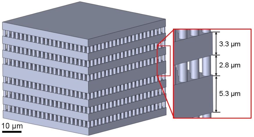
One-dimensional photonic crystals composed of alternating layers of high- and low-density (see
Figure 1) were designed using stratified-layer optical model calculations (WVASE32, J.A. Woollam, Co., Lincoln, NE, USA). Alternating dielectric layers were produced using a two-photon polymerization-compatible polymer IP-Dip. The dielectric properties of the compact layers
are described by means of the parameterized model-dielectric-function of polymerized IP-Dip. The model-dielectric-function of this material has been previously established using spectroscopic ellipsometry in the infrared spectral range and is described using a simple mixed oscillator model [
29].
The low-density layers consist of sub-wavelength cylindrical pillars which are arranged in a square lattice pattern and are oriented normal to the low-density/high-density interface. The dielectric function of the low-density layers
can be described using the Bruggeman effective medium approximation given by [
30]:
The dielectric properties of the inclusions and the host medium are then given by
and
, respectively. In our design the host medium is air, i.e.,
, whereas the inclusions consist of polymerized IP-Dip
. The volume ratio between the cylindrical inclusions and the host medium is described by the volumetric fill factor
.
The effect of a high-density defect layer is explored by comparing the infrared optical response of two photonic crystals. Using simple stratified-layer optical model calculations, the photonic bandgaps of the photonic crystals are designed to be centered at
= 2556 cm
(
= 3.91 µm). The selection of the wavelength for the photonic bandgaps is based on the dielectric function of IP-Dip, which offers a transparent window in the range from 2000 to 3000 cm
[
29]. One crystal is composed of 6 alternating high- and low-density layers. The thicknesses of the high- and low-density layers are designed to be 3.3 µm and 2.8 µm, respectively, as shown in
Figure 1. The volumetric fill factor
of the low-density layers is
. The second crystal is identical to the first crystal except for the introduction of a high-density defect layer in the center of the layer stack. The high-density defect layer has a thickness of 5.3 µm and consists of compact polymerized IP-Dip. The base of both photonic crystals is designed to be 49.2 µm × 49.2 µm.
A commercial two-photon polymerization system (Photonic Professional GT, Nanoscribe, GmbH) was used to polymerize a single monomer (IP-Dip) in order to fabricate the one-dimensional photonic crystal structures on a fused silica substrate. It is very well known that the voxel size depends on a number of parameters, such as the objective, choice of monomer, laser power, scan speed, and hatching and slicing distances, for instance [
25,
26,
27,
28]. Thus, the identification of parameters which permit the true-to-design fabrication of complex structures can be difficult and time consuming.
For the photonic crystals discussed here, the volume-to-surface ratios between the low-density and high-density layers differ substantially. As a result, low- and high-density layers are affected differently by the solvent-diffusion-based swelling/contraction which occurs during the rinsing/drying process after the polymerization. This fabrication problem is resolved here by introducing a one-dimensional geometric scaling factor , which provides a layer thickness scaling that is different for high- and low-density layers. The scaling factors were determined using photonic crystals without defects, but with otherwise identical designs. For the high-density layers = 0.92 and for the low-density layers = 1.30 was used.
Following the fabrication, the structures are rinsed in propylene glycol monomethyl ether acetate for 10 min, 99.99% isopropyl alcohol for 10 min, and then left to air dry for at least 30 min. A 63× objective lens with laser power at 20 mW and scan speed at 500 mm/s was used. Both slicing distance and hatching distance were set to 0.2 µm.
Infrared reflection measurements were carried out for all photonic crystals in the spectral range from 2000 cm
to 3000 cm
with ra esolution of 2 cm
using an IR microscope (HYPERION 3000 Bruker, Inc., Billerica, MA, USA) in combination with an FTIR spectrometer (VERTEX 70, Bruker, Inc.). An IR microscope with an annular collection aperture was equipped with a Mercury-Cadmium-Telluride detector. A 15× Cassegrain objective with confocal illumination was used with an aperture setting of 20 µm, resulting in an angular spread of 0.6° with an average angle of incidence of 8.7°. All reflection measurements were normalized to a bulk gold sample using the same aperture settings as those employed during the sample data acquisition. A silicon carbide globar was used as a light source. All measurements were performed at room temperature. Stratified-layer optical model calculations obtained using WVASE32 (J.A. Woollam Co., Lincoln, NE, USA) were employed to analyze the reflection measurements. SEM images, shown in
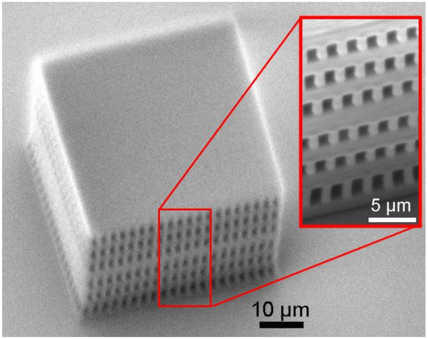
Figure 2 independently demonstrated the quality of the fabrication and the resulting true-to-design dimensions of the fabricated photonic crystal.
3. Results and Discussion
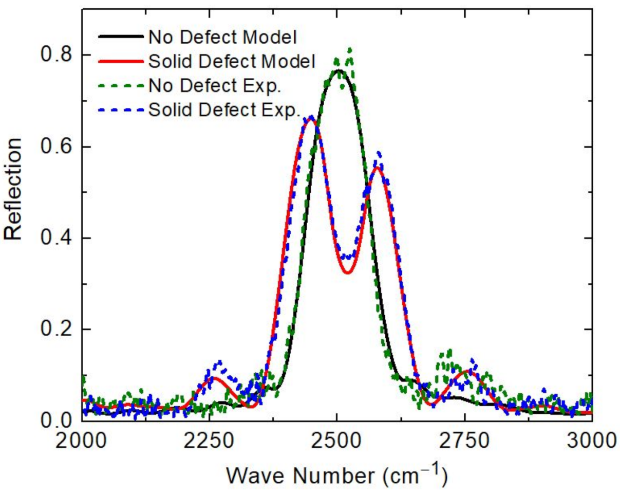
The experimental reflection data (dashed lines) and best-model calculated reflection data (solid lines) for both crystals are depicted in
Figure 3. The major spectral feature is the photonic bandgap, which is centered at 2500 cm
for both photonic crystals. For the photonic crystals with the solid layer defect, a defect mode is formed in the center of the photonic bandgap. The reflection amplitude of the photonic crystal without a defect is 77%; with a high-density defect layer this amplitude is reduced to 62%. The defect mode of the photonic crystal with a high-density defect layer is centered at 2520 cm
and has a reflection amplitude of 26% with respect to the average bandgap maxima of 62%. A very good agreement was found between the best-fit stratified-layer optical model calculations (solid lines) and the experimental reflection measurements (dashed lines) for both photonic crystals.
The optical model is composed of 14 layers: a fused silica substrate, six A-B layer pairs of low- and high-density layers, and a high-density defect layer in the center, following the design shown in
Figure 1. The dielectric functions of the glass substrate and IP-Dip used here were previously determined using spectroscopic ellipsometry and were not varied in the model [
29,
31]. Equation (
1) is used to determine the dielectric function of the low-density layers. During the data analysis, geometrical model parameters were varied simultaneously, including: the layer thickness of the low- and high-density layers, layer thickness non-uniformity, and volumetric fill fraction
. All parameters were adjusted using a Levenberg–Marquardt-based algorithm until the best match between the model-calculated and experimental reflection data set was obtained. Note that the experimental data sets of both photonic crystals were analyzed simultaneously in order to reduce parameter correlations. The best-model thickness of the low-density layers was determined to be (2.771 ± 0.014) µm, the high-density to be (3.311 ± 0.010) µm, and the high-density defect layer to be (5.240 ± 0.015) µm. The best-model volumetric fill factor was found to be
= 0.296 ± 0.007. In order to model the experimental reflection data accurately, layer thickness non-uniformities were taken into account and found to be an average of (2.8 ± 0.1)% for all layers.
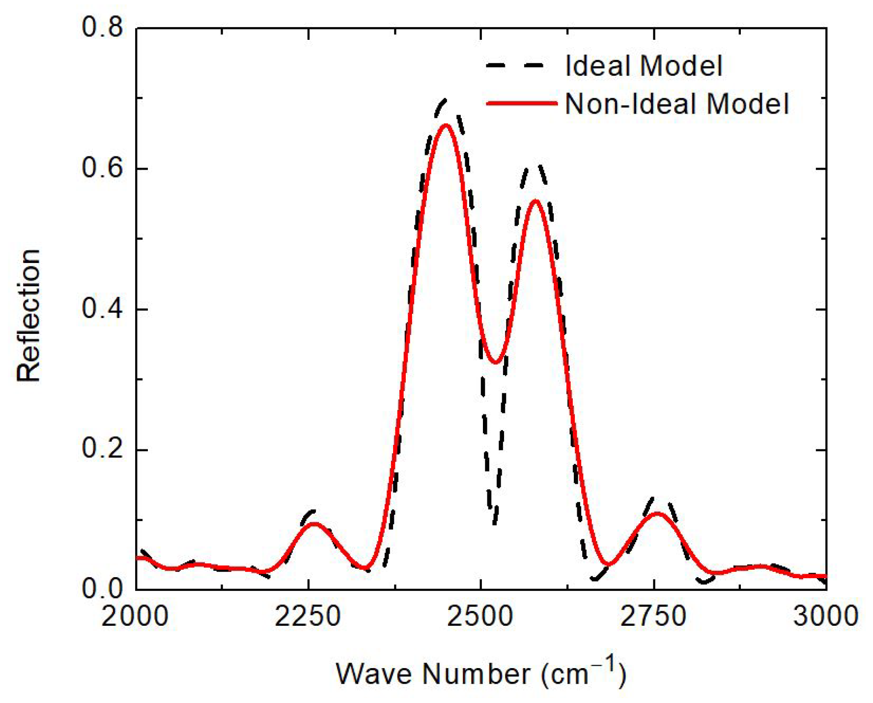
The effect of this non-uniformity on the defect mode is illustrated in
Figure 4, where stratified-layer optical model calculations for two photonic crystals with a defect are compared. The spectrum plotted with a black dashed line depicts the model-calculated reflection obtained assuming ideal interfaces and the red solid line assumes a 2.8% layer thickness non-uniformity. A photonic bandgap with a centered defect mode can be seen for both models; however, the amplitude of both the photonic bandgap and the defect mode is diminished for the photonic crystal with non-ideal interfaces. The reflection amplitude of the defect mode with perfect layer uniformity is 56%, whereas the amplitude with a 2.8% layer thickness non-uniformity is 26%. Additionally, the average photonic bandgap magnitude is reduced by approximately 5.6% with this non-uniformity present. Our experimental findings corroborate the theoretical calculations conducted by T.S. Perova et al. [
8], which have shown that layer thickness non-uniformities induce a reduction in the bandgap amplitude similar to what is seen in
Figure 4.
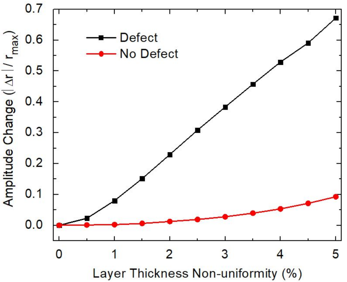
The influence of the layer thickness non-uniformity on the defect mode amplitude is shown in
Figure 5. A comparison is made between the changes in the photonic bandgap amplitude in a photonic crystal without a defect and the defect mode amplitude in a photonic crystal with a defect with respect to layer thickness non-uniformity. The changes in amplitude are normalized to the maximum reflection of the photonic bandgap in the photonic crystal with no defect and ideal, abrupt, plane-parallel interfaces. The change in amplitude of the defect mode is more significant for increasing layer thickness non-uniformity compared to that for the photonic bandgap. This trend continues up to a non-uniformity of 5% at which point the defect mode becomes indistinguishable.
4. Conclusions
A one-dimensional photonic crystal with a solid, compact, defect layer was successfully fabricated via direct laser writing with two-photon polymerization. After determining and introducing one-dimensional geometric scaling factors for the low- and high-density layers, two photonic crystals were fabricated, which were identical except for the addition of a defect layer in one. For both crystals, a photonic bandgap was identified experimentally. The photonic bandgap is centered at 2500 cm. In the photonic crystal with a defect layer, a defect mode was induced in the middle of the the photonic bandgap.
Our stratified-layer optical model calculations are in a very good agreement with the experimental results. Best-model thickness values are in a very good agreement with the nominal design parameters. When the scaling factor () was implemented, a stratified-layer optical analysis of the reflection data from these photonic crystals reveals best-model layer thicknesses within ±1.2% of our nominal design values. In introducing scaling factors, we take into account not only the voxel size, but the entire effect of the two-photon polymerization, rinsing, and drying process, which results in the final geometry. Even minute changes in layer thickness non-uniformity had substantial effects on the amplitude of the defect mode. For the photonic bandgap these amplitude changes were not as pronounced. This sensitivity can be used to determine layer thickness non-uniformity in one-dimensional photonic crystals fabricated for the infrared spectral range by means of two-photon polymerization. The volumetric fill factor for the low-density layers was found to be 9.6% larger than designed. Although having minimal effects on the shape of spectral features, this change resulted in a shift of the photonic bandgap from the designed 2556 cm to 2500 cm. Note that the scaling factor was omitted for the volumetric fill factor, which explains the substantial deviation from its nominal value. This deviation may be reduced by introducing a separate scaling factor.
By introducing density-dependent scaling factors in the design phase we have enabled the fabrication of one-dimensional photonic crystals with defect modes which have true-to-design layer thicknesses. In contrast to determining the layer thicknesses, the interface roughness (layer thickness non-uniformity) is difficult to assess. Therefore, one-dimensional photonic crystals engineered with narrow band defect modes may provide a method to quantify this important fabrication parameter. One-dimensional photonic crystals with defect modes demonstrate features that are relevant for applications as narrow band filters [
20]. In addition, photonic crystals show promise as enhanced Faraday rotators [
4], omnidirectional bandgap filters [
5], and sensors [
18,
19].


