Abstract
With power designers always demanding for faster power switches, electromagnetic interference has become an issue of primary concern. As known, the commutation of power transistors is the main cause of the electromagnetic noise, which can be worsened by the presence of unwanted oscillations superimposed onto the switching waveforms. This work proposes a solution to mitigate the oscillations caused by the turn-on of a power transistor by exploiting its source inductance plus an external one. In this context, an optimization method is proposed to find the optimal value of the source inductance as a trade-off between oscillation damping and power dissipation. The experimental results performed on a prototyped power converter assess the proposed technique as the spectrum of the conducted emission is attenuated by 20 dB at the oscillation frequency. With respect to traditional solution based on snubbers, the proposed solution results in a similar oscillation damping, but with a 0.5% higher power efficiency.
1. Introduction
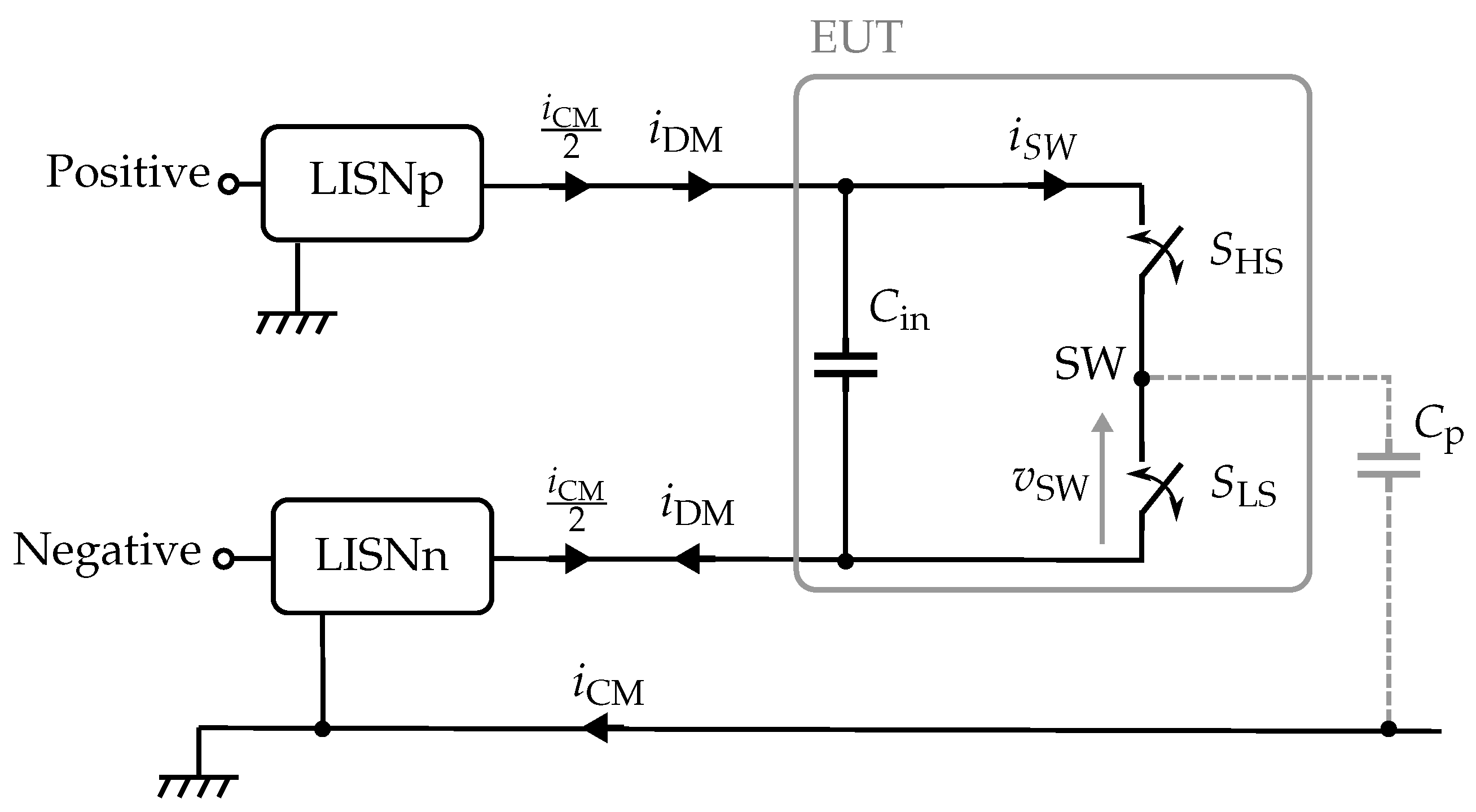
The continuous progress of semiconductor technologies has made possible the fabrication of increasingly faster power transistors to be used in switched power applications, e.g., motor inverters and DC–DC converters. Indeed, power designers can benefit from lower on-resistance, higher switching frequency, and smaller heat-sinks, all resulting in converter designs with higher power density. Although the pros of using more performing power switches are valuable, they are counteracted by the higher level of electromagnetic interference (EMI) they deliver, which can be attenuated quite hardly. Such an aspect can not be neglected by practitioners, since, in order for any electronic equipment to be placed on the market, it must comply with electromagnetic compatibility (EMC) standards in accordance with national or international legislation. Amongst the required EMC tests, the measurement of conducted emission aims to assess the noise current, which is delivered by the equipment under test (EUT) and it is conducted back onto the power supply system, to be within given limits. A general description of the test setup used for measuring the conducted emissions is shown in Figure 1, where in between each power line and the EUT power supply terminal, a line impedance stabilization network (LISN) is inserted to have the impedance shown by the power supply network univocally defined over the frequency range of interest.
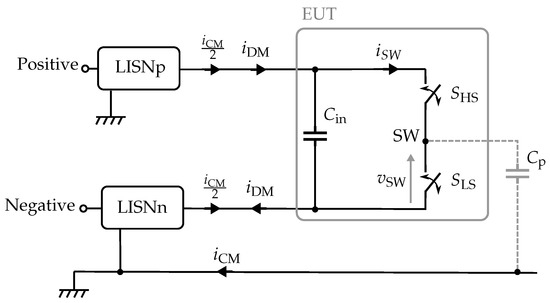
Figure 1.
Conducted emission setup for a single leg. The differential- mode (DM) and common-mode (CM) currents are highlighted, as well as their major sources, i.e., the switching current () and the switching voltage (), respectively.
As far as switched power circuits are concerned, the half-bridge is identified as a root element from the EMC viewpoint, since the switched operation of the active devices it is made of, i.e., transistors and diodes, is the primary cause of the conducted disturbance current [1,2]. The EUT shown in Figure 1 is modeled as a single leg and an input capacitance, which provides the switching current during the commutations of the and power switches. The power supply network shown in Figure 1 is a three-conductor system, thus the current flowing in the positive and in the negative lines can be expressed in terms of a differential-mode (DM) component () and a common-mode (CM) component (). The former is due to the parasitics of the input capacitor that cause high-frequency components not to flow in entirely, resulting in a DM current provided by the power line. The latter () is the current that flows in the ground conductor and it is related to the affecting the node, which causes a current to flow in the parasitic capacitance . As far as the half-bridge shown in Figure 1 is concerned, it is possible to identify the primary sources of EM noise as the switching current () for the DM EMI, and the switching voltage () for the CM EMI. The magnitude of the CM current usually increases with frequency as the impedance shown by the parasitic capacitance decreases, and usually, it dominates over the DM emission in the mid-frequency range [3], i.e., from 1 MHz to 30 MHz, where the regulatory limits are stricter. As a result, the mitigation of conducted EMI (CE) is definitely a key issue, as higher , caused by faster power switch, results in higher emission levels.
Since the switching voltage () is the major source of conducted EMI, its frequency spectrum allows one to predict the CE, provided that the propagation path is known. As far as hard-switched power circuits are concerned, such a voltage can be approximated by a trapezoidal waveform, whose pulse-width () corresponds to the on-time of and its high value equals to the DC voltage across . Even though more accurate models can be considered, as in [4], where multiple slopes are accounted for during commutations, the trapezoidal approximation results in an upper boundary of the frequency spectrum magnitude [5]. Indeed, under the assumption that the rise time equals the fall time, i.e., the envelope of a trapezoidal waveform is characterized by two break frequencies, at and [6]. Since typically , it is , meaning that determines the high-frequency spectral content of the CM source voltage, and of the CE, eventually.
Actually, the switching voltage () can be affected by oscillations taking place during the switches turn-on and turn-off. More precisely, such oscillations are triggered by voltage or current steps exciting resonant circuits, which comprise the capacitive and the inductive parasitics of the power switches themselves, of the package interconnections and of the printed circuit board (PCB) layout. As a consequence, peaks at the resonant frequencies can appear in the frequency spectrum, as well as in the one, eventually. The superimposed oscillations also affect radiated emission, as reported in [7,8], thus they must be definitely avoided.
Standard solutions to reduce the amplitude of such oscillations include the use of resistor-capacitor (RC) snubbers [9], ferrite beads or to slow down transients by means of a higher output resistance of the driver. Although the aforementioned techniques are effective in avoiding such unwanted oscillations and in reducing the delivered EMI by decreasing the dV/dt [10], on the other side, the switching losses of the power switches increase significantly, resulting in a lower efficiency of the power circuit [11,12]. For such a reason, new solutions to find a better trade-off between EMI reduction and efficiency are currently being investigated. Amongst them, the use of active gate drivers (AGD) has been proven to be effective in controlling the switching trajectories of power transistors, resulting in a better compromise between overshoot reduction and switching power losses [13,14,15]. The key idea of AGDs is to modify the strength of the driver during the turn-on and the turn-off of power transistors, more precisely, it is required to slow down the transistor in the middle of the commutation, while keeping fast the remainder part of the transition [16]. In such a way, the transistor itself is exploited as a dissipative element, meaning that instead of driving it from a very high resistance, i.e., the off state, to a very low resistance, i.e., the on state, it is driven to modulate its output resistance during the commutation to avoid the oscillations from taking place. However, AGDs suffer from some major cons, as they require a complex hardware, they are not commercially available, and their tuning may be challenging to achieve if no feedback is exploited [17]. The switching waveforms obtained using an AGD can be closely reproduced using a simpler and cheaper passive component available on the market. The key idea of the work presented in this paper is to modulate the driver strength of a high-side power transistor without using an AGD, but exploiting the source inductance. Indeed, during the transistor turn-on, such an inductance couples the power loop with the driver loop, so that the control voltage of the transistor is reduced during the transient, as in the case of an AGD. As a consequence, the switching waveforms are differently shaped with respect to a conventional gate driver, and the oscillations resulting from the excited parasitic resonant circuit are reduced. The proposed technique aims to reduce the CE delivered by a power circuit where high-side transistors are exploited, focusing on the reduction in the unwanted oscillations that take place during the high-side transistor turn-on by means of the source inductance.
The paper is organized as follows: in Section 2 the source and the propagation path of CM conducted emissions are discussed in the case of a half-bridge, and a simplified model is presented. Then, in Section 3, the switching waveforms of such a leg are reported in case of a conventional gate driver and of an AGD. Section 4 introduces the effect of the source inductance and the feedback during the transistor turn-on is discussed. Then, in Section 5, simulations on the prototyped converter are reported to investigate more deeply the source inductance effect, and a method to find its optimal value is proposed. Finally, in Section 6, the experimental results are presented, and a comparison between the proposed technique and the use of a snubber is performed both in terms of CM EMI mitigation and efficiency. Concluding remarks are drawn in Section 7.
2. Common-Mode Conducted Emissions of Power Switching Circuits
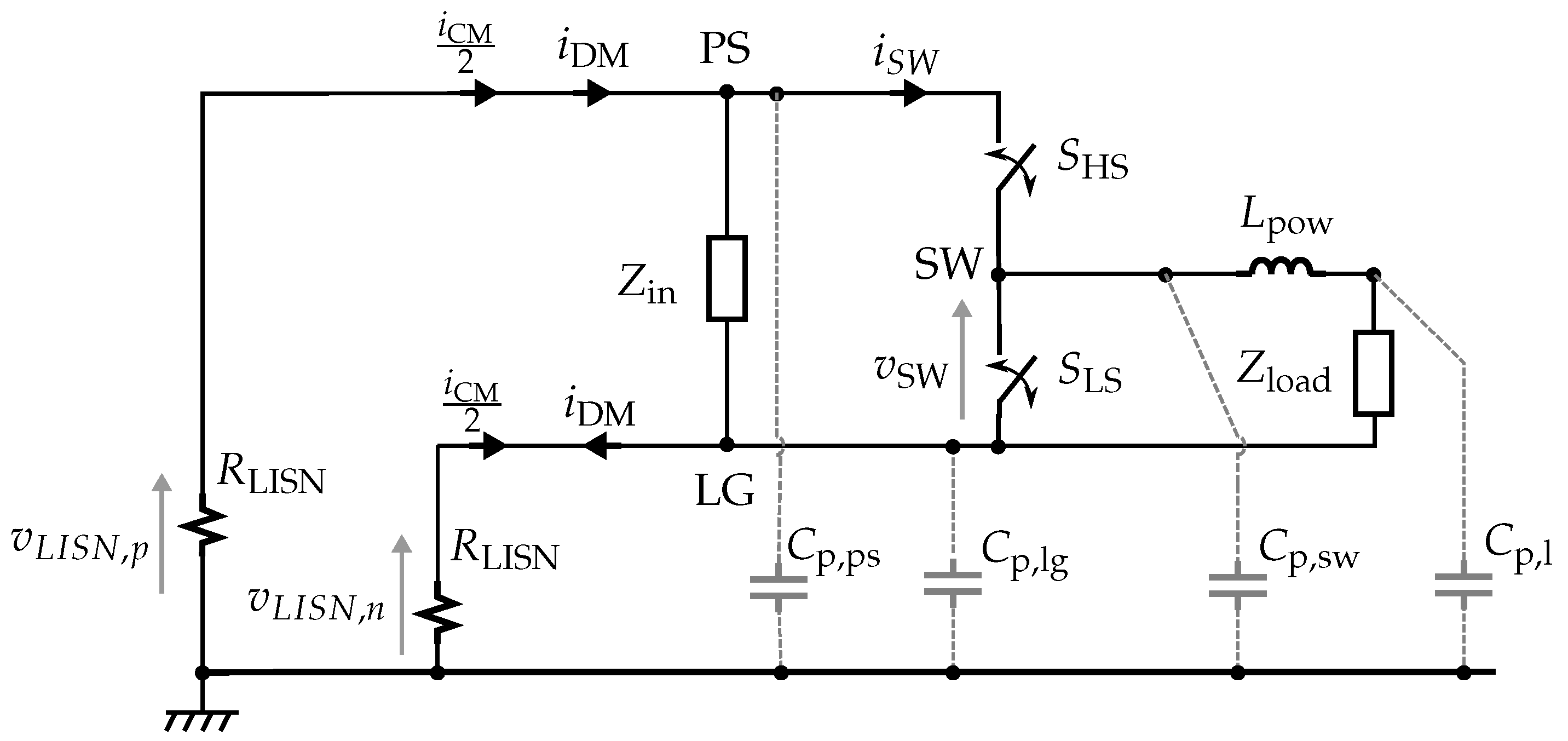
The source and the propagation path of the CM EMI delivered by a switching circuit are discussed in this Section. The analysis is carried out referring to the circuit shown in Figure 2. The EUT comprises input capacitors represented by the impedance, ideal high-side () and low-side () switches, which are connected to the output load impedance through the inductor . In order to simplify the analysis of the CM EMI, the EUT terminals are loaded with the LISNs impedance, which can be approximated by a resistance in the frequency range of interest. Finally, the parasitic capacitances that load the EUT nodes toward the reference ground plane are indicated with dashed lines to be distinguished from the other components. More precisely, connects the negative input terminal (node ) of the EUT, the positive input terminal (), the switching node and the load to the ground plane. Moreover, the CM current (), the DM current (), the switching current (), and the voltage across the low-side switch (), which have been previously defined on Figure 1, are depicted too.
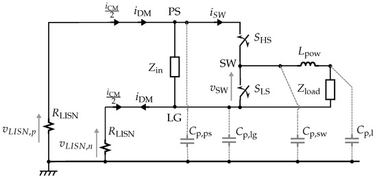
Figure 2.
Single leg circuit including the impedance of the line impedance stabilization network () and the parasitic capacitances, connected by dashed lined, to the ground plane.
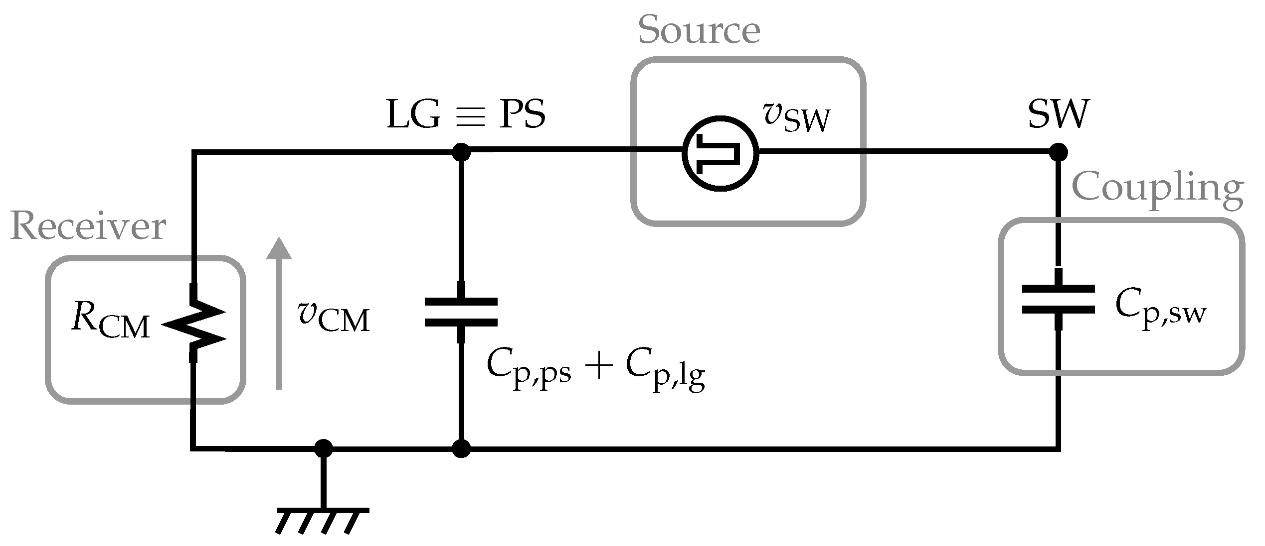
As previously mentioned, the DM current is mainly due to the switching current , whereas to the switching voltage , resulting in a current to flow in . In order to simplify further the model shown in Figure 2 for the analysis of the CM EMI, the DM current is not taken into account, i.e., . This condition is valid only if , meaning that the switching current flows completely in the input capacitors. As far as the CM EMI is concerned, the node is short-circuited to the node and the impedance shown by the two LISNs is equal to . Under these assumptions, the only current loop involved in the CM EMI is the one that comprises the LISN impedances, the low-side switch and the capacitances . Such a loop is redrawn in Figure 3, where the noise source , the capacitive coupling and the EMI receiver are clearly identified. By definition, the CM EMI voltage is equal to
where and are the voltages across the measurement ports of the two LISNs, as shown in Figure 2. The frequency spectrum of , denoted as in what follows, is related to the frequency spectrum of the switching voltage according to
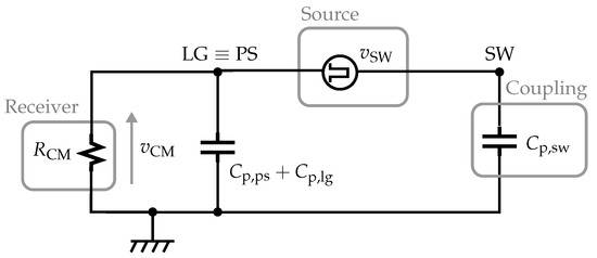
Figure 3.
Equivalent circuit for the analysis of the CM electro-magnetic interference (EMI) in a half-bridge. The source voltage corresponds to the switching voltage , the coupling is due to the parasitic capacitance and the receiver is modeled by the LISNs equivalent impedance.
Typically it is , thus the magnitude of the CM transfer function () can be approximated by its numerator for , meaning that is the only capacitance that contributes to the CM EMI in the frequency range of interest. Equation (2) ideally allows one to predict the CM EMI provided that the frequency spectrum of and the values of the parasitic capacitances are known. An upper bound for the frequency spectrum is provided by the trapezoidal approximation, whereas, the value of can be either extracted by analytical formula if the geometry is simple, as in [1], or by using finite element simulators [18]. Moreover, (2) states that the CM EMI can be mitigated either by reducing the spectral content of , by decreasing , or by increasing .
3. Time Domain Analysis of the CM Voltage Source
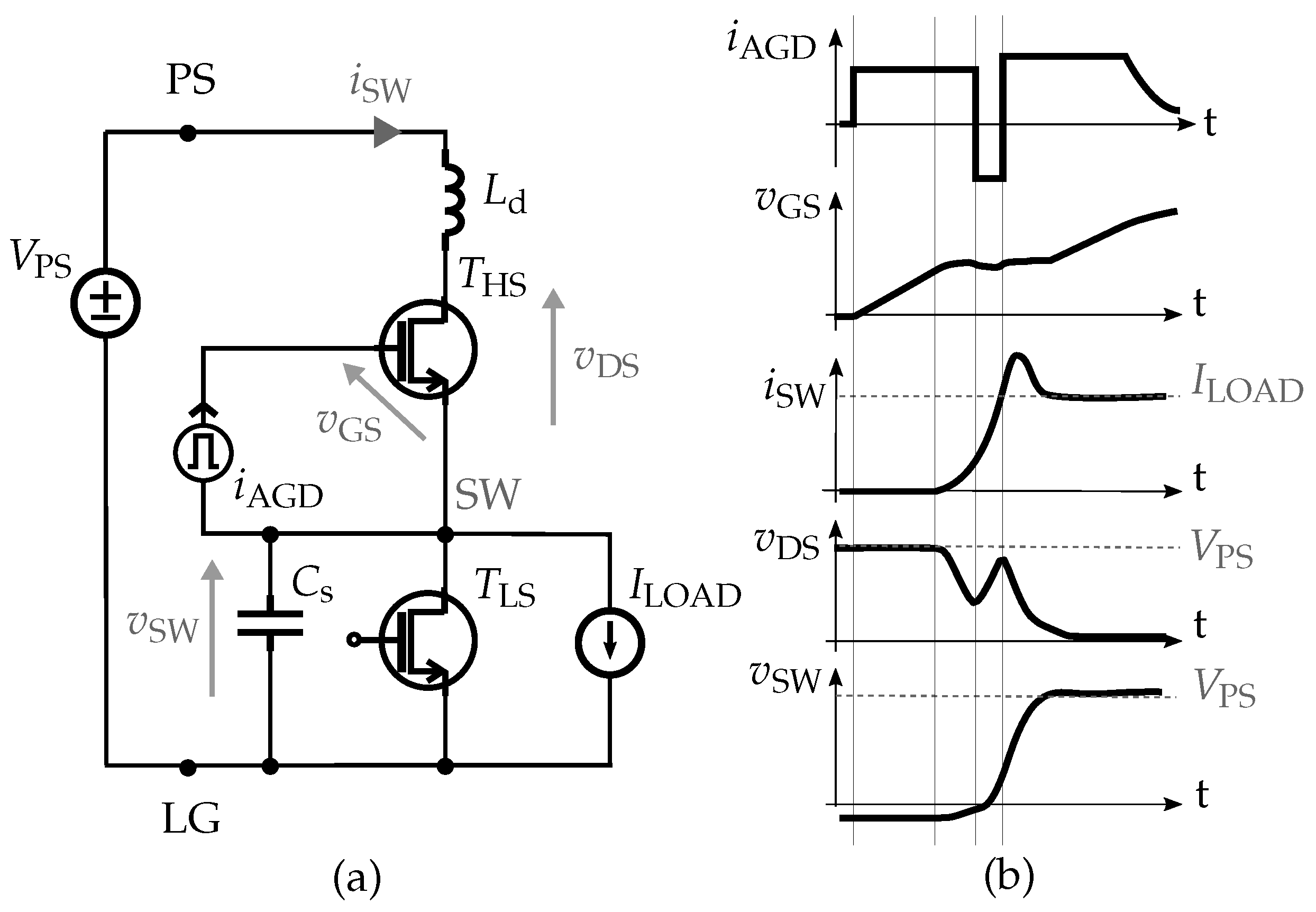
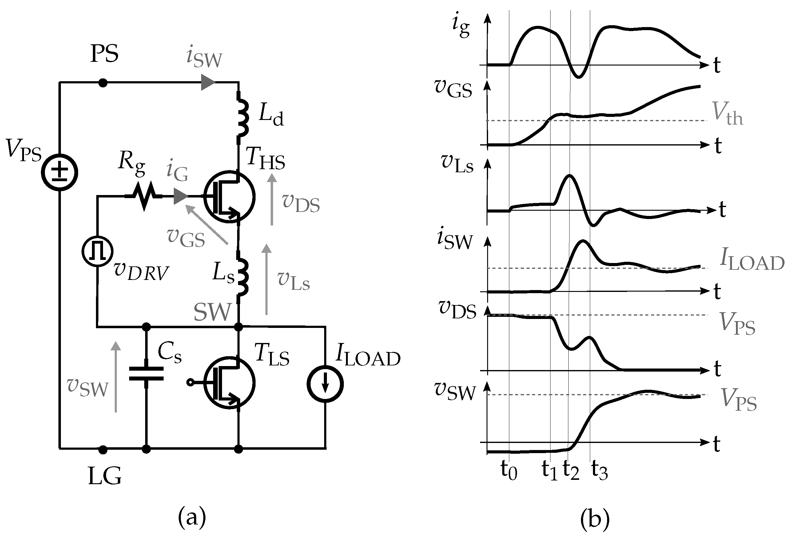
From what presented so far, the source of CM emission in a half-bridge is the voltage across the low-side power switch (), as it causes a CM current to flow in the parasitic capacitance and a CM voltage on the EMI receiver, eventually. Before introducing the source inductance and its effect on , it is convenient to introduce a detail description of the phenomena taking place during the high-side transistor turn-on. Such analysis allows one to identify the resonant circuit excited during the turn-on transient, more precisely, the circuit shown in Figure 4a is considered. The high-side transistor is driven by a conventional gate driver (CGD) comprising of an ideal square wave voltage generator () and the gate resistance (), and it is complemented by the low-side transistor (). The power inductor () is modeled by the current sinker , since the current flowing in is subjected to much slower variations with respect to the taking place during the transition [19].
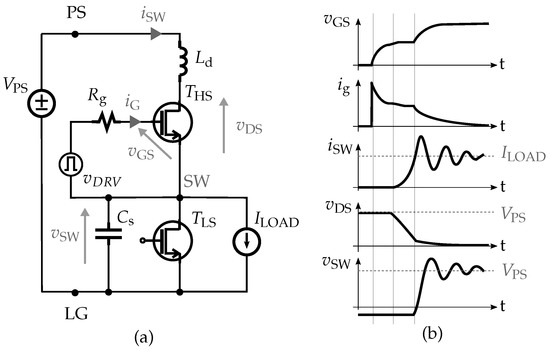
Figure 4.
(a) Simplified model of a single leg for the analysis of the turn-on when the high-side transistor is driven by a convention gate driver and (b) the corresponding switching waveforms.
In addition, the active devices, the parasitic inductance , which includes both the package interconnections and the PCB traces, is considered, as well as the parasitic capacitance between and , which is due to the PCB layout. Referring to the corresponding switching waveforms shown in Figure 4b, the positive edge triggers the turn-on, and after the gate source voltage () overcomes its threshold voltage, a positive current () flows in , resulting in a linear decrease in the drain-source voltage (). To avoid a cross-conduction current to flow in and , the low-side transistor is assumed to be already turned-off when the positive edge of occurs, meaning that only its body diode should be considered in what follows.
When the current reaches the value , the low-side body diode turns-off and the voltage increases, eventually. In this phase, the diode can be modeled through its junction capacitance , which is in parallel to the parasitic capacitance of the PCB layout () since it is reverse biased, resulting in a series LC resonator with the inductance . More precisely, the voltage across the capacitances, i.e., , must be charged to . Such a voltage step may excite the resonator, and result in oscillations affecting both the switching voltage () and the switching current () at the frequency, which is equal to
The damping factor characterizing the resonator depends on the resistive components, more precisely on the parasitic resistance of the interconnections, which is typically negligible, and the on-resistance of , provided that it is in triode when the oscillation takes place.
In addition to the use of CGD, active gate drivers (AGDs) have proofed to be effective in controlling the switching trajectories of power switches. A constant-piecewise current generator is used for modeling the AGD, as shown in Figure 5a. The corresponding switching waveforms are shown in Figure 5b under the assumption that the gate current profile causes the voltage to be critically damped, meaning that it avoids the oscillation from taking place while keeping the overall transient as fast as possible [20]. Indeed, the gate current affects the voltage when the transistor is in the Miller region, since the slope (S) of is given by
where is the drain-gate capacitance of [21]. The reduction in the slope by means of a smaller gate current, or even a negative one, results in a still in saturation during the rising of the voltage . This means that by controlling the voltage through the gate current, the oscillation can be avoided since the transistor itself is used as a dissipative element. Although dissipates more power with respect to the CGD solution [22], it prevents the energy bouncing between the inductive and capacitive elements of the resonator from taking place.

Figure 5.
(a) Simplified model of a single leg for the analysis of the turn-on when the high-side transistor is driven by an active gate driver generating a current modulation, and (b) the corresponding switching waveforms.
4. Transistor Feedback through the Source Inductance
With the aim of investigating the effects of the source inductance, the analyzed circuit is shown in Figure 6a, where the topology previously shown in Figure 4a is complemented with the source inductance , and the corresponding switching waveforms are shown in Figure 6b. In , the rising edge of triggers the turn-on, so the voltage starts to increase up to reach its threshold value at . The input driver loop comprises a series RLC circuit, i.e., the inductance in series with the input capacitance . At , enters its saturation region, thus increases, as well as the voltage across (), across (), and the voltage eventually decreases. Under the hypothesis that the voltage is approximately constant due to the Miller’s effect, the KVL in the input driver loop results in
meaning that, if increases, then decreases. The gate current decreases up to reach in . It is worth noticing that, even though the gate current is negative, is still in saturation provided that . This point () also corresponds to a maximum on and . From , comes negative, thus . The drain current, however, will still increase up to reach its peak value, in . This corresponds to , i.e., a concavity change. From on, the current is again positive, thus . The transistor will exit the Miller’s plateau and enter the triode region, eventually.

Figure 6.
(a) Simplified model of a single leg for the analysis of the turn-on when the high-side transistor is driven by a convention gate driver and the source inductance is considered, and (b) the corresponding switching waveforms.
Depending on the value of and of the and parasitics, the negative feedback introduced by can slow down the transistor and suppress the oscillations. Even though the power dissipation of the high-side transistor increases when an extra source inductance is inserted [23], it prevents the oscillation from taking place.
The exploitation of the source inductance to mitigate the turn-on oscillations, however, comes at the cost of worsening the switching performance during the turn-off, as highlighted in [24,25,26]. Indeed, the unavoidable presence of the source inductance and of the gate-drain capacitance is the root cause of a cross-talk phenomenon between the input loop (gate driver) and the output loop (power loop). The most dangerous side effect of this crosstalk is the self turn-on at the turn-off transient [27], which may result in self-sustained undampened oscillations [28]. The self turn-on phenomenon takes place when the transistor is already off, i.e., , but the current flowing in the drain-gate parasitic capacitance () drives the gate voltage above the threshold [27]. However, such a phenomenon can be avoided by a proper choice of the gate driver resistance, as discussed in what follows.
5. Simulation Results
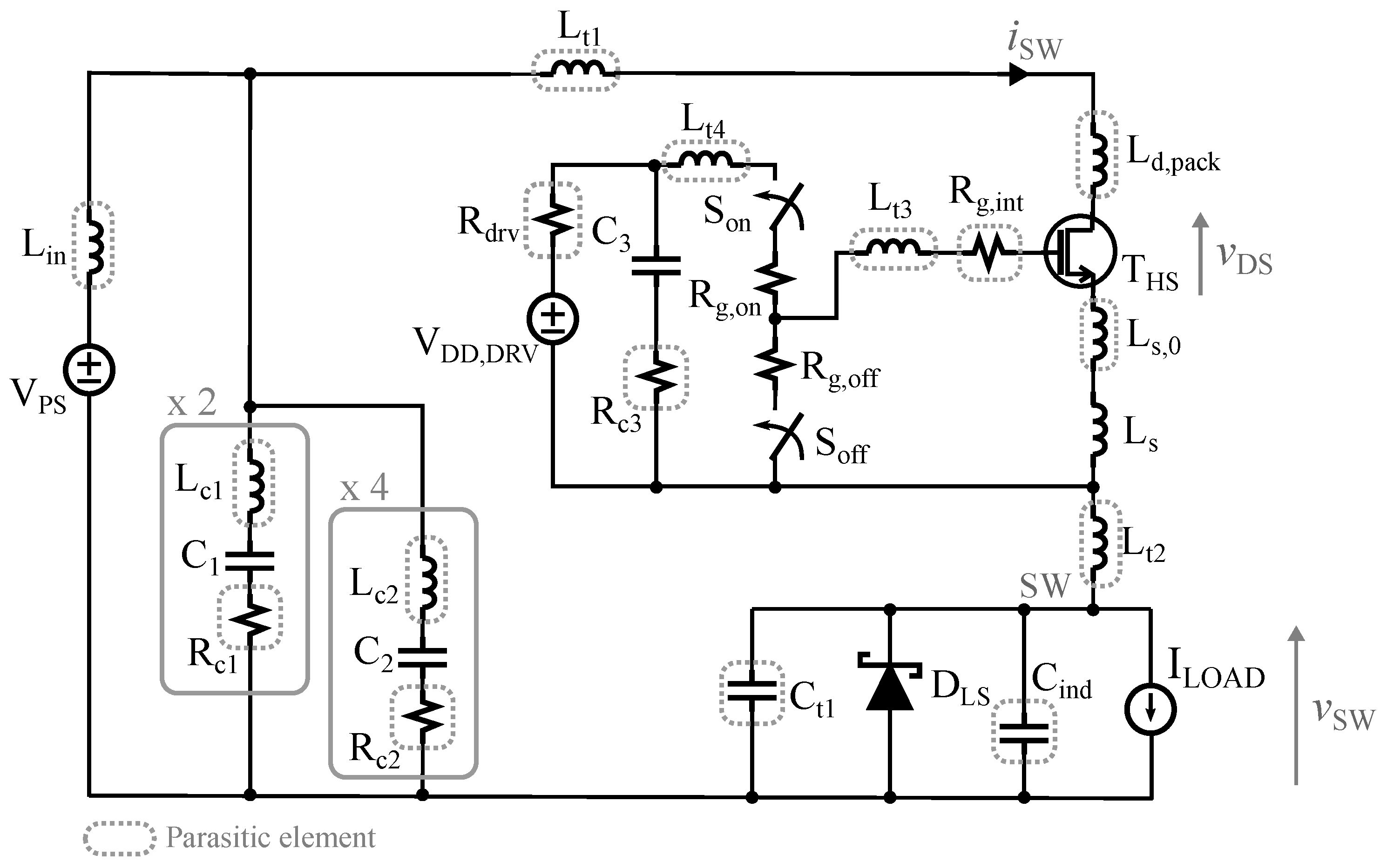
Aiming to further investigate the effect of the source inductance on the switching waveforms during the transients and to provide a method to obtain the optimal value, time-domain simulations were carried out on the circuit shown in Figure 7. It models an asynchronous Buck converter, which was lately prototyped and exploited as EUT in Section 6. Such a converter was designed to step down an input voltage () of 48 V to a 12 V output voltage, and it is able to provide the load with a maximum current of 5 A. The high-side transistor () is periodically turned on and turned off with a 0.25 fixed duty cycle and 150 kHz fixed switching frequency by the switches , , that model the gate driver output stage. The converter is provided with a set of input () capacitors, which lower the voltage ripple affecting the input voltage, and a freewheeling diode , which allows the output current to flow when is off. The simulated schematic, which is shown in Figure 7, comprise the active and the passive devices, as well as the parasitics, which are encircled in dashed boxed to be found at a glance. The parasitics of the PCB traces () were evaluated from the extraction of the scattering parameters of the PCB by means of a 3D electro-magnetic simulator, models the parasitic capacitance of the power inductor, which are not shown in Figure 7, and it was evaluated from its resonant frequency provided by the manufacturer. The internal gate resistance of is equal to its nominal value, and the driver resistances are discrete level components which can be modified. The values of the adopted components are listed in Table 1.
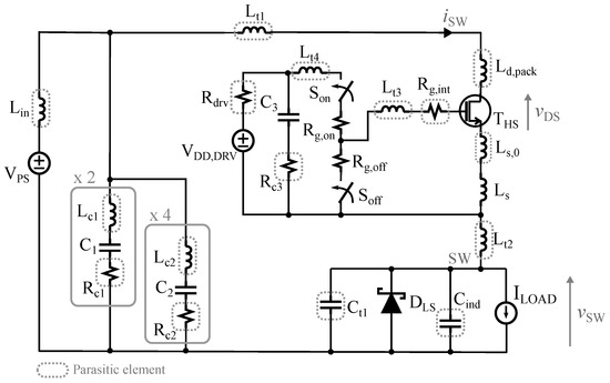
Figure 7.
Power stage of the designed step-down Buck converter, including the active () and the passive () devices. Parasitics due to printed circuit board (PCB) traces, packages and non-idealities of the passive components are enclosed in dashed boxes.

Table 1.
Parameter values of the simulated converter.
5.1. Turn-On Analysis
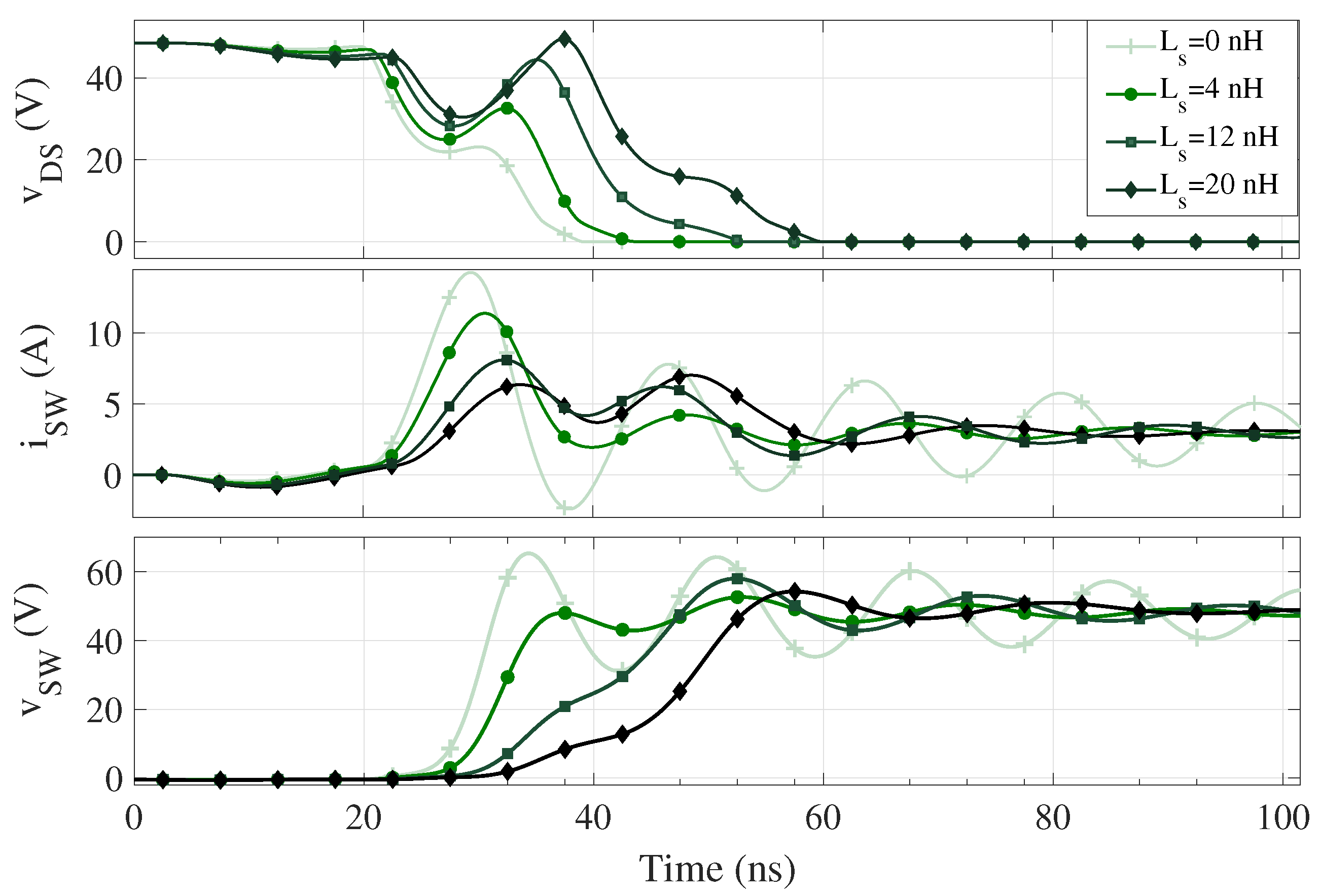
As far as the turn on is concerned, if the high-side transistor is driven sharply and no damping technique is exploited, i.e., , the switching waveforms obtained from the time-domain simulation of the circuit in Figure 7, are shown in Figure 8 by plus markers. Indeed, both the switching current () and voltage () are affected by oscillations at MHz. The corresponding voltage is not monotonic due to the parasitic, which is however not sufficiently large to damp the oscillations. If an extra source inductance () is added, both the peak and the damping factor decrease with respect to the oscillating case, as for (circle markers), (square markers) and (diamond markers). From such plots, it can been noticed that the higher the is, the more the voltage increases during the transient as the gate current is negative for a longer time. At the same time, the rise time and the peak, which is needed to charge the equivalent low-side capacitance to , both decrease as increases. Finally, from the comparison of the 4 nH and 12 nH curves, it results that a higher value does not imply a more damped oscillation. All such aspects suggest one that the optimal value of source inductance for the simulated converter is in between 4 nH (circle markers) and 12 nH (square markers), as the rise time of is not significantly affected by the source inductance and the oscillations are strongly reduced with respect to the oscillating case.
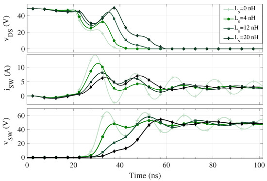
Figure 8.
Switching waveforms at the turn-on in the oscillating case (plus markers), and with a 4 nH (circle), 12 nH (square) and 20 nH (diamond markers) inductances obtained from a time-domain simulation of the circuit shown in Figure 7.
5.2. Optimization Method
In order to find the optimal value of source inductance to be inserted in the power loop, the method discussed hereafter is proposed. By performing parametric simulations on the value of the circuit shown in Figure 8, and according to [23], it resulted that the switching energy at the turn-on () linearly increase with , as shown in Figure 9 by the dashed line. Conversely, the frequency spectrum should be compared against some target to determine whether the turn-on resonance is undamped or overly damped. In what follows, the frequency spectrum of an ideal trapezoidal waveform, with the same pulse-width, rise and fall time of the obtained from the simulation, is chosen as a target. The envelopes of the frequency spectrum (), obtained for the different values, were evaluated and each of them compared against the corresponding envelope of the ideal trapezoidal frequency spectrum (), which was obtained from [6]. Then, the ratio () between the envelope obtained from the simulation and the target one was evaluated at the turn-on resonant frequency as,
where MHz is to account for uncertainties and the resonant frequency was evaluated as
since it decreases with . For the EMI viewpoint, the optimal value of is the one with , as the corresponding switching waveform is the fastest and non-oscillating. The maximum ratio between such spectra was evaluated for in the (0,34) nH range and it is shown in Figure 9 by solid line. In the case of no source inductance added (), the frequency peak is approximately 15 dB higher than the expected one, and two point with exist, i.e., and . As is 3 in the case of , which is approximately 1.4 times smaller than in the 22 nH case, the optimal value of source inductance is = 6 nH.
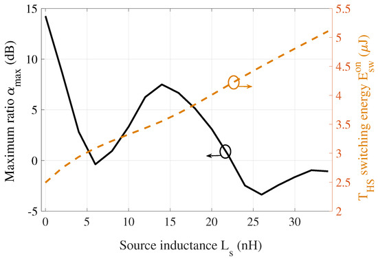
Figure 9.
Switching energy related to during its turn-on (dashed line) and the maximum ratio between the and the ideal trapezoidal waveform spectra.
5.3. Turn-Off Analysis
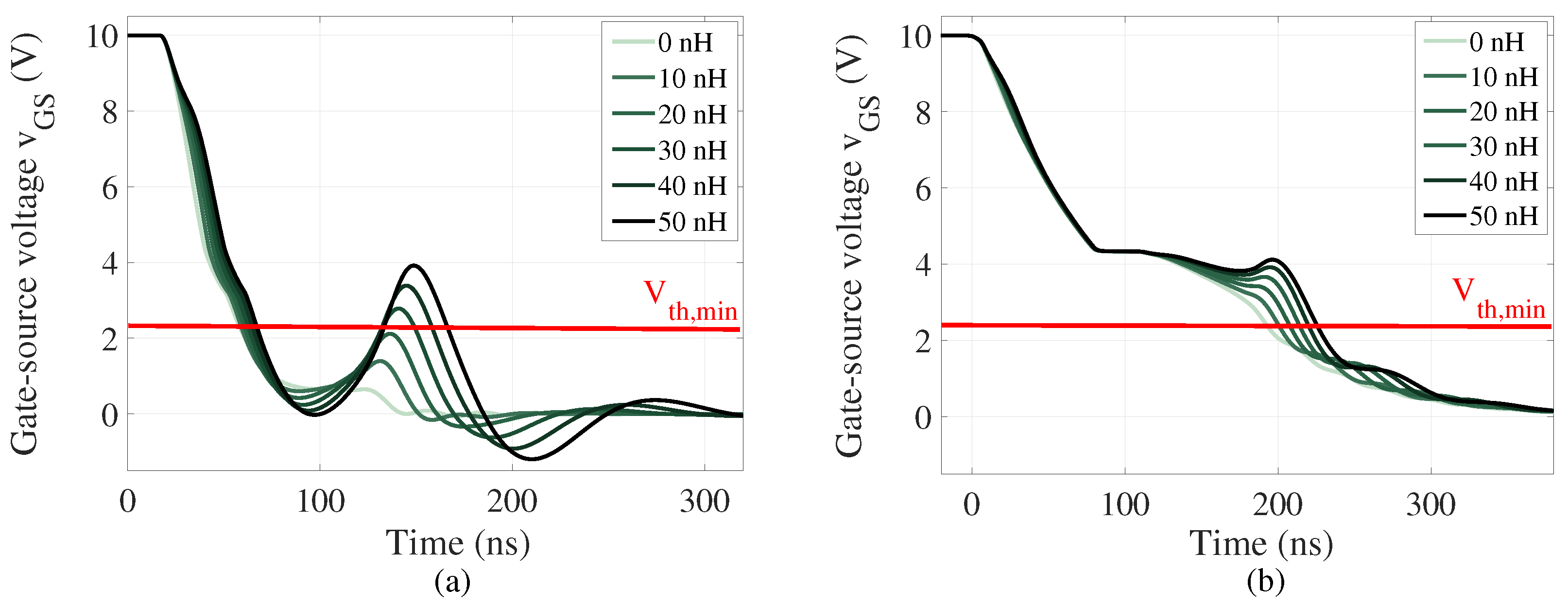
Although the proposed technique is effective in damping the turn on oscillation, an increase in the source inductance may lead to the self turn-on of during its turn off. The circuit shown in Figure 7 was simulated to deep such an aspect, resulting in the voltages shown in Figure 10a with and . It is worth noticing that the increases once is off as the causes the to be negative, thus, if the voltage across the gate inductance is neglected, it is
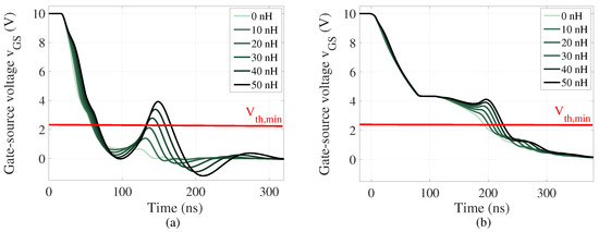
Figure 10.
The gate-source voltage at the turn off with (a) = 0 and (b) = 10 for .
If is higher than the transistor threshold, the self-turn on phenomenon occurs. As far as the considered circuit is concerned, , thus the source inductance should be lower than 30 nH, resulting in the optimal value not to be sufficiently high to cause such an issue. However, if the source value found from the optimization method would have been higher, (8) states that the voltage drop across the gate resistance counteracts the effect of the source inductance, meaning that the gate resistance at the turn-off can be increased to avoid the self turn-on. More precisely, if is increased up to 10 , the corresponding voltages are shown in Figure 10b. In addition to the presence of the Miller’s plateau, it can be noticed that no self turn-on event occurs even in the case of nH, however, the power dissipation during the turn-off of the high-side transistor increases.
6. Experimental Results
Aiming to check the validity of what presented so far, experimental measurements were carried out on the Buck converter introduced in Section 5. The switching waveforms were acquired for different values of source inductance, and frequency spectrum of the switching voltage was evaluated to assess the reduction in the peak corresponding to the turn-on oscillation. Then, a setup compliant to the CISPR-25 [31] standard was used, and the CM EMI was measured, assessing the optimal value of source inductance found in Section 5.2. Different operating conditions of the Buck converter were also tested to verify the effectiveness of the technique in a real-case scenario. Finally, the proposed solution was compared against the traditional one, i.e., the use of a low-side snubber, resulting in almost the same spectra reduction, but in a higher efficiency.
6.1. Switching Waveforms
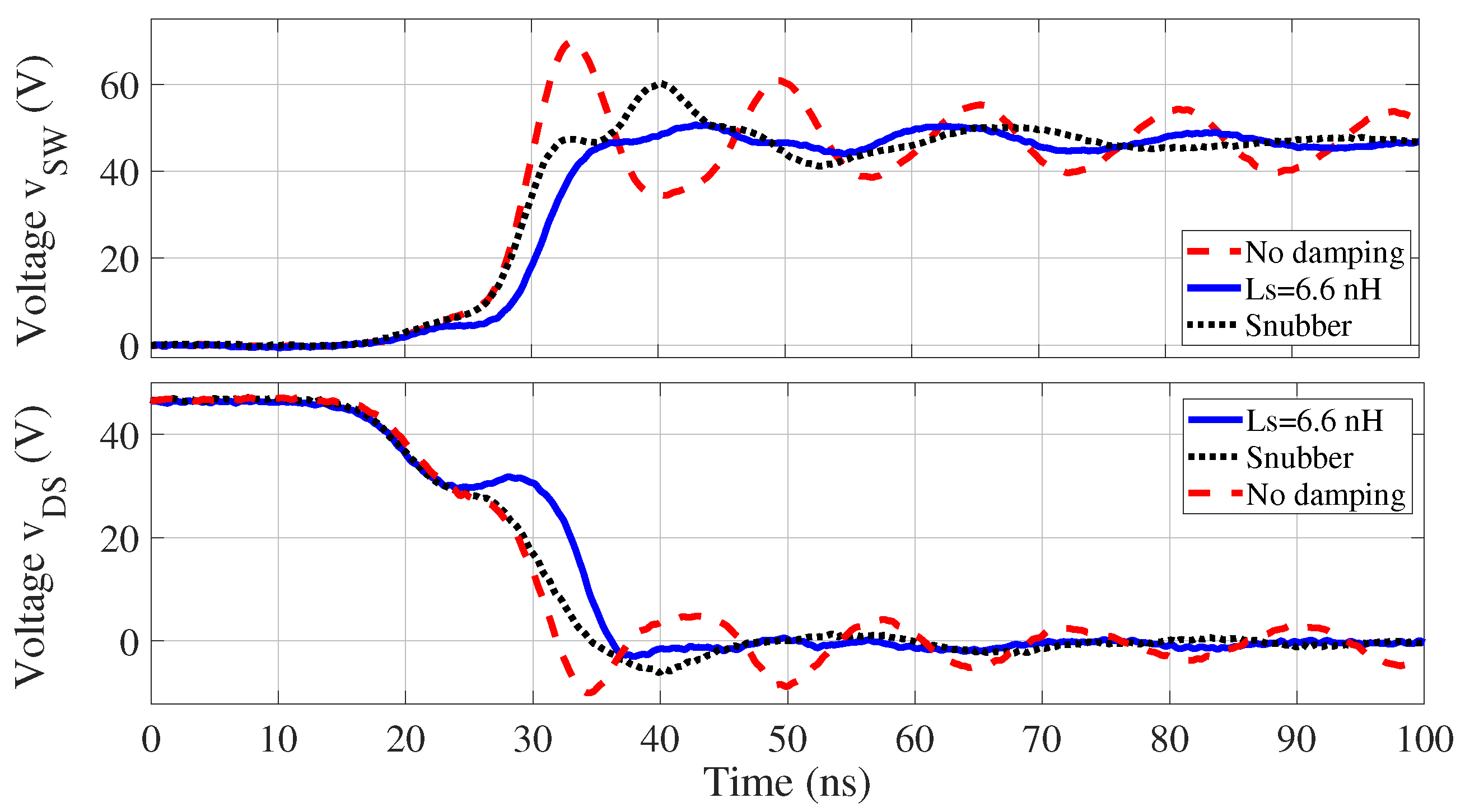
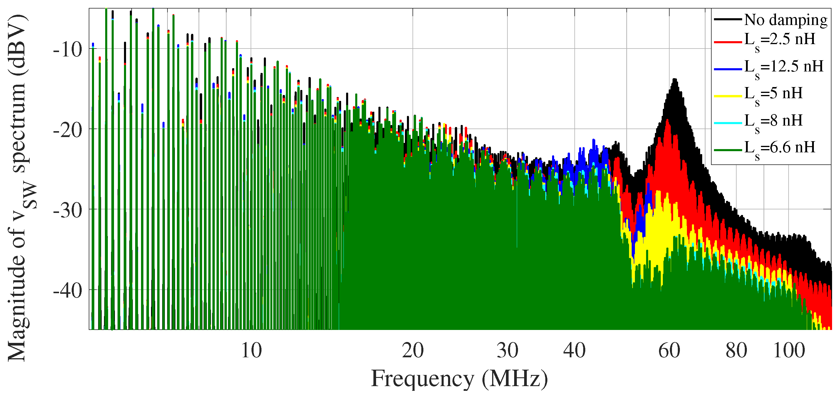
If no damping solutions are exploited, the switching voltage (), which was measured by means of a digital oscilloscope, is affected by oscillations at the turn-on, as shown in Figure 11 by dashed lines. More precisely, the oscillation takes place after the voltage has dropped off. Such an oscillation is characterized by MHz and a peak equals to 69 V. At the turn-off, a negligible oscillation with MHz and 50.4 V peak is superimposed onto . To damp the turn-on oscillation, a low-side RC snubber, which was characterized by [9], was inserted, resulting in the switching waveforms shown by dotted lines in Figure 11. The snubber effectively removes the oscillations, but it slightly slows down the rise during the turn-off. Then, the snubber was removed and a 6.6 nH air core wrapped inductor, which was the closest value available on the market to the optimal value found previously, i.e., nH, was exploited as source inductance. The corresponding switching waveforms are those shown by solid lines in Figure 11. Indeed, the peak voltage is reduced and the oscillations are almost completely damped with respect to the undamped case. Referring to Figure 11, the voltage is not monotonic when the source inductance is inserted, i.e., during the Miller’s plateau the high-side transistor is slowed-down by the negative feedback introduced by the source inductance. Moreover, during the turn-off no unwanted self-turn-on is present, as expected. Different values of source inductance were tested, i.e., and the magnitudes of the corresponding frequency spectrum in the (5, 100) MHz frequency range are plotted in Figure 12 in case of an output current equals to 3 A. When the high-side transistor is driven sharply, the peak at the frequency is noteworthy, on the contrary, the one related to the turn-off is not apparent. The spectrum comprises a secondary peak at 48 MHz, approximately 10 dB lower than the one at , which is also related to the turn on. Indeed, from the waveform in Figure 11a in dashed line, it can been noticed that the turn-on oscillation is not purely sinusoidal, but it is distorted, meaning that higher order resonant circuits are excited. Such spectra validate the optimal value found in Section 5.2, as the peak is reduced by 20 dB. Indeed, lower values, i.e., 2.5 nH and 5 nH, result in a peak not completely removed, whereas the 8 nH spectrum is equal to the 6.6 nH one, meaning that there are no advantages in the use of a higher source inductance. Indeed, if is further increased up to 12.5 nH, the peak at increases again, which is also in agreement with the simulations, as reported in Figure 8 by square markers.
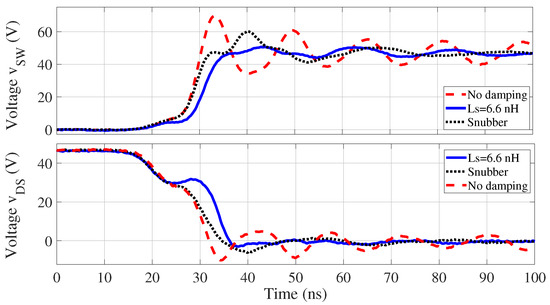
Figure 11.
Measured time domain phase voltage (a) and drain-source voltage () (b) at the turn-on. The dashed lines were obtained in the oscillating case, the dotted ones with the low-side snubber inserted and the continuous ones with a 6.6 nH source inductance. The use of the source inductance allows one to reduce the over-voltage affecting the at the turn-on.
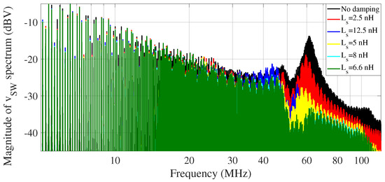
Figure 12.
Frequency spectra of the measured switching voltage () with 3 A output current and different source inductances.
6.2. CM Conducted Emission
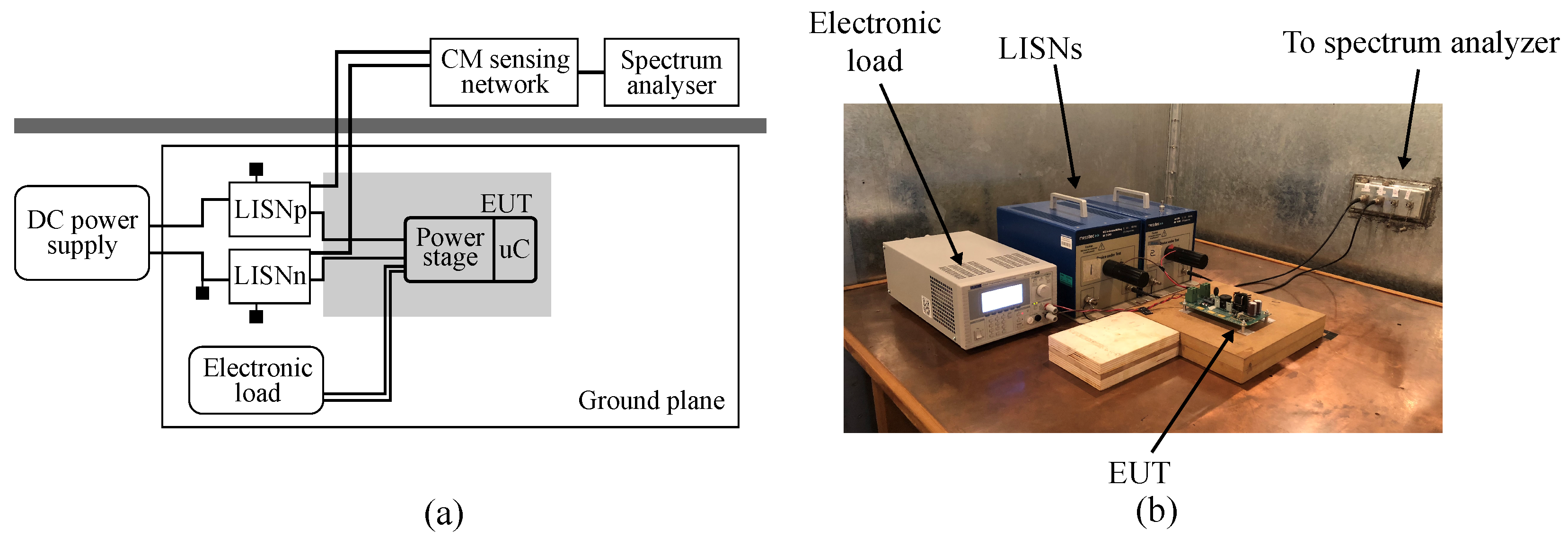
In order to measure the CM EMI delivered by the Buck converter, the setup recommended in the CISPR-25 standard [31] was adopted. Such a test-bench is sketched in Figure 13a (not in scale), and the common-mode EMI was measured by means of the CM sensing network described in [32]. Two LISNs were exploited since the power supply cables are 20 cm long. A picture of the experimental setup is shown in Figure 13b, where the key components are labeled too. The load, which is connected to the output port of the Buck converter, is an electronic load operating as variable resistance, so different values of output current can be tested.
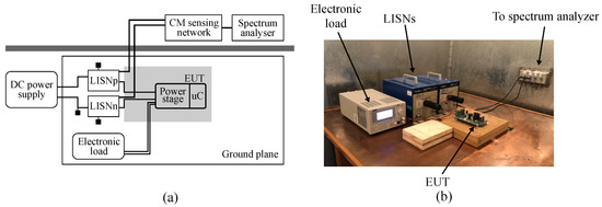
Figure 13.
(a) Block diagram of the test setup to measure the common-mode EMI delivered by the device under test (DUT), and (b) a photograph of the experimental setup compliant with CISPR-25 standard.
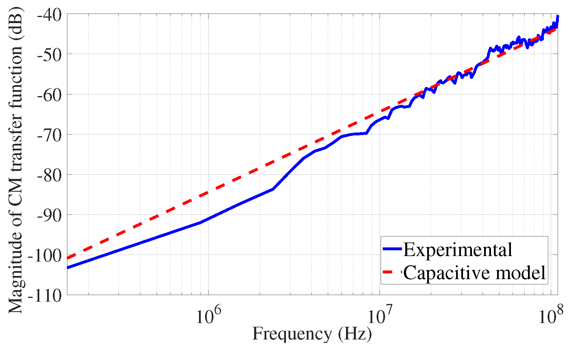
In order to verify that the CM conducted EMI are related to the switching voltage () through a capacitive coupling, as previously described in Section 2, the frequency spectrum of the switching voltage () was subtracted from the spectrum of the common mode voltage () measured using the spectrum analyzer. Then, the magnitude of the transfer function was evaluated at each frequency as
where G = 5.4 dB is the attenuation introduced by the CM sensing network. The envelope is shown in Figure 14 by solid line. By fitting such an envelope with a straight line having a slope of 20 dB/dec, the dashed curve is obtained. It is worth noticing that even though the propagation path can be complex, in actual fact the equivalent model presented in Section 2 is effective. As far as the designed Buck converter is concerned, from the straight line approximation it is possible to estimate the equivalent parasitic capacitance, resulting in .
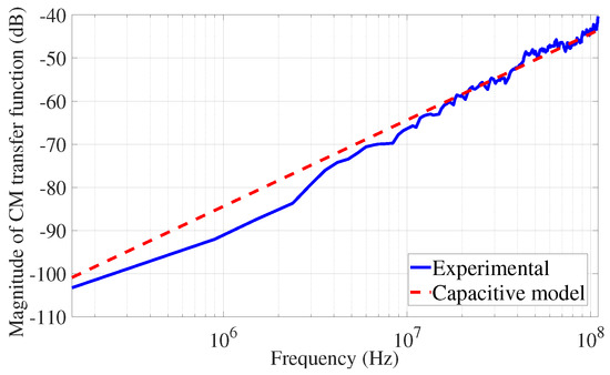
Figure 14.
Common-mode transfer function obtained by experimental results (continuous line) and the fitted one (dashed line). The capacitive model is effective in predicting the CM EMI propagation.
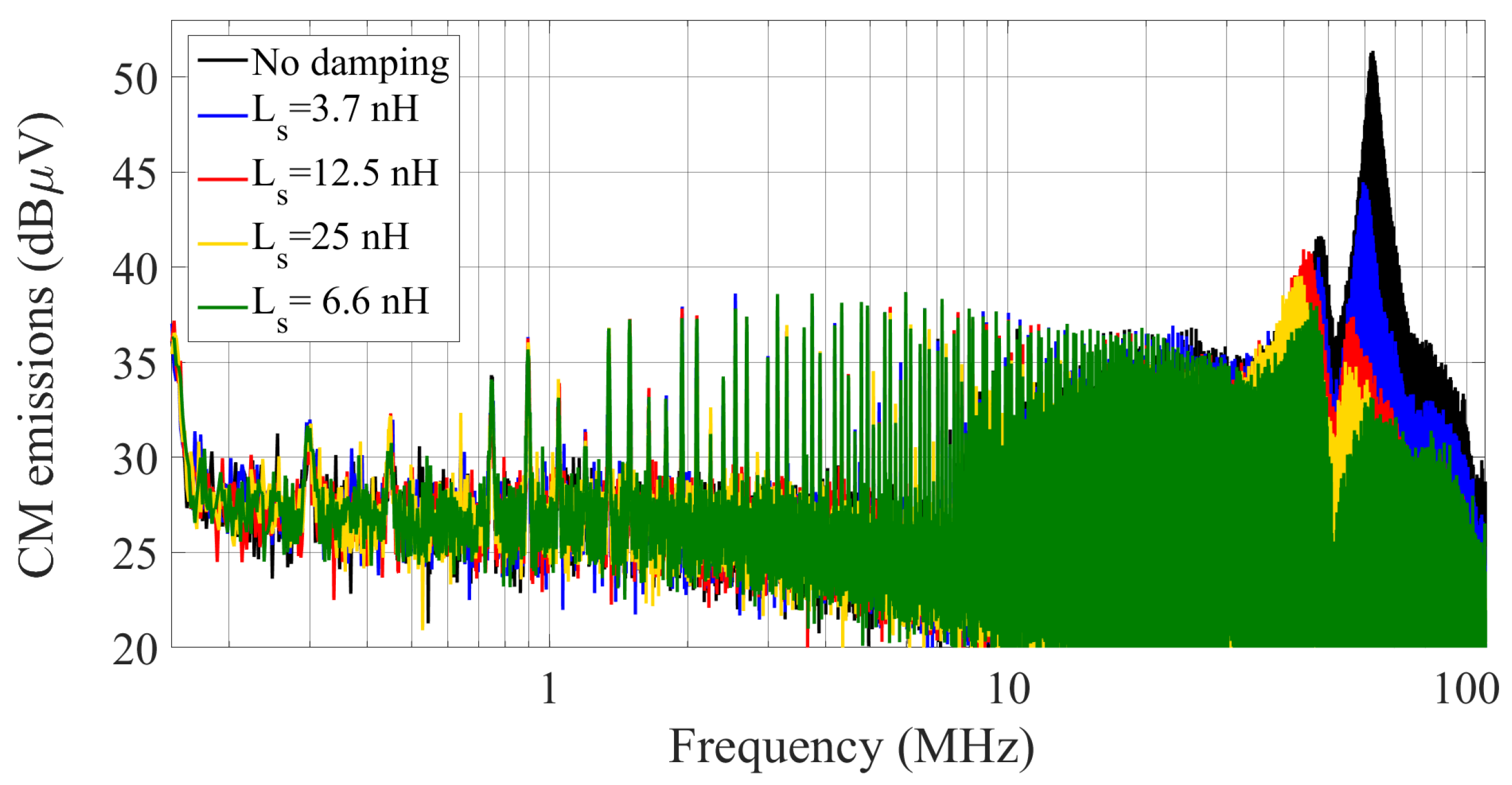
Once the capacitive coupling was assessed, the common-mode EMI was measured for different values of source inductance, as shown in Figure 15 for a load current equals to 3 A. More precisely, surface mounted air core inductors, with nominal values of , were exploited to test the proposed technique. As it can be noticed from Figure 15, the use of the source inductance is effective in reducing the peak caused by the turn-on oscillation, as well as the spectral components in the (60 MHz, 90 MHz) frequency range. Indeed, by increasing the value of the source inductance from 3.7 nH up to 25 nH, the peak at moves to lower frequencies and its amplitude is reduced. More precisely, in case of 3 A output current and = 6.6 nH, the peak is approximately 20 dB lower than the oscillating case. Such an aspect assess the effectiveness of the proposed technique, since the insertion of the source inductance introduces a negative feedback during the transistor turns-on, and modifies the switching voltage, eventually.
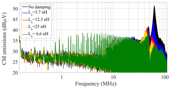
Figure 15.
Measured CM of the designed Buck converter with 3 A output current, no damping and different values () of the source inductance. The value corresponds to the optimal case.
6.3. Sensitivity to the Operating Conditions
As far as the proposed technique is concerned, the effect of the load current and the input voltage were further investigated to assess its effectiveness in a real case scenario. The CM EMI shown in Figure 16a refers to different values of output current, more precisely 1, 2, 3, 4, 5 A, with the source inductance fixed to its optimal value, i.e., = 6.6 nH. As previously mentioned, such a value of source inductance is optimal for = 3 A, whereas lower and higher values of current result in higher CM EMI. More precisely, for a 2 A and 5 A output current, the frequency peak is 5 dB higher than in the optimal case, whereas, for = 1 A, it is 10 dB higher. In any case, the worst case, i.e., = 1 A, corresponds to a peak reduction with respect to the oscillating case of 10 dB, which is not negligible. As far as input voltage variations are concerned, the corresponding CM EMI are shown in Figure 16b for = 36, 42, 48, 52 V. Indeed, variations on the input voltage results in a different junction capacitance of the Schottky diode as the reverse voltage across changes, meaning that the values of the equivalent resonant circuit are modified with respect to the nominal case, i.e., = 48 V. Additionally, in this case, the 6.6 nH source inductance does not completely removed the peak at for input voltage values lower than the nominal one, even though its is strongly reduced with respect to the oscillating case.
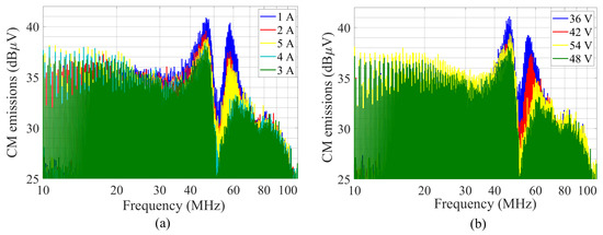
Figure 16.
Sensitivity of the CM EMI with respect to (a) different load current (1 A, 2 A, 3 A, 4 A, and 5 A), and (b) different input voltage (36 V, 42 V, 48 V, 54 V) with a 6.6 nH source inductance.
6.4. DM Conducted Emissions
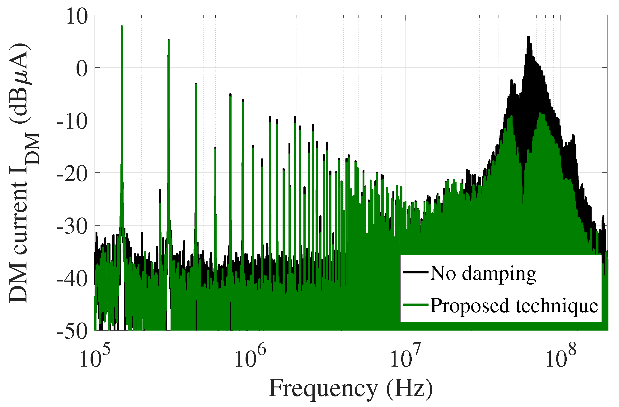
Since the oscillations affecting at the turn on are strongly reduced with the proposed technique, as shown in Figure 8, and since the main source of DM conducted emissions is the switching current itself, then the proposed technique is expected to reduce the DM EMI too. Aiming to assess such a point, the DM current was evaluated as
where are the voltages acquired by a digital oscilloscope at the measurement ports of the two LISNs loaded with 50 and = 100 is the equivalent DM mode resistance [33]. The frequency spectrum of was evaluated, resulting in the spectra shown in Figure 17 for the oscillating and the 6.6 nH source inductance inserted. From such spectra it can be noticed that the proposed technique allows one to reduce the turn-on peak of the DM EMI by 15 dB, which is a noteworthy result.
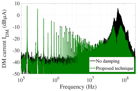
Figure 17.
Spectra of the DM conducted current obtained from the time-domain voltages at the line impedance stabilization networks (LISNs) measurement port with no damping and with the proposed technique.
6.5. Comparison with RC Snubber
Finally, the proposed technique was compared against the use of a RC snubber in terms of common-mode emissions. More precisely, the frequency spectra of the corresponding CM EMI are shown in Figure 18a in case of a 3 A load current. The source inductance was fixed to 6.6 nH, which corresponds to the optimal value for a 3 A output current. In such a case, the source inductance and the snubber solution both remove the turn on peak altogether. As far as power circuits are concerned, the efficiency should be the highest as possible. Since the power dissipated by active devices is strongly affected the switching power, i.e., during the turn-on and the turn-off transients, also the efficiency will be affected by the switching transients. The conversion efficiency () is considered as a figure of merit in what follows, and it can be evaluated as the ratio between the output and the input power of the converter. More precisely, it is
where () is the average voltage (current) provided by the input supply voltage to the EUT, whether () the average voltage (current) provided by the EUT to the load. Such quantities can be evaluated by means of DC voltmeters and ammeters placed in parallel and in series to the input and output ports of the DC–DC converter. The results are plotted in Figure 18b for different setups. It is worth noticing that the no damping solution (circle marker) results in the higher efficiency (85.5%), which is reasonable as the transients are the fastest. The snubber solution, which effectively damps the oscillation and reduces the CM EMI, result in a 84.77% efficiency, meaning that the frequency peak at is cancelled at the cost of 0.8% lower efficiency. The proposed solution, on the other hand, results in an efficiency of 85.2%. Such a result validates a better trade-off between EMI reduction and efficiency of the proposed solution with respect to the snubber one.
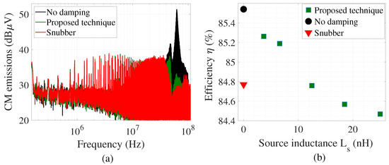
Figure 18.
(a) CM EMI delivered by the design Buck in case of no damping, snubber inserted and 6.6 nH source inductance, and in (b) the conversion efficiency.
7. Conclusions
In this paper, the use of the source inductance to mitigate the conducted EMI in power switching circuits is investigated. The source and the propagation of CE are analyzed referring to a half-bridge topology, from which it results that the voltage across the low-side power switch is the major source. Such a voltage can be affected by unwanted oscillations after the turns-on and the turns-off of power switches, which can be avoided by using AGDs. This work aims to reduce the amplitude of such oscillations by means of the source inductance, as a negative feedback takes place during the turn-on, thus avoiding complex AGDs. An optimization method is proposed to obtain the optimal value of source inductance, resulting in a trade-off between extra switching power losses and CE Experimental results assess the validity of the proposed technique both in case of switching waveforms and measured CE, resulting in a 20 dB CM EMI and 15 dB DM EMI attenuation at the turn-on oscillation frequency. Finally, a comparison with a snubber was performed, resulting in similar EMI mitigation but in a 0.5% higher efficiency.
Author Contributions
Conceptualization, F.F.; methodology, E.R., F.F.; validation, E.R.; investigation, E.R.; writing E.R., F.F.; supervision, F.F. All authors have read and agreed to the published version of the manuscript.
Funding
This research received no external funding.
Institutional Review Board Statement
Not applicable.
Informed Consent Statement
Not applicable.
Acknowledgments
The authors would like to thank Matteo Vincenzo Quitadamo for his helpful advice during the preliminary analysis. The work was partially supported by the Power Electronics Innovation Center, Politecnico di Torino, Italy.
Conflicts of Interest
The authors declare no conflict of interest.
References
- Laour, M.; Tahmi, R.; Vollaire, C. Modeling and Analysis of Conducted and Radiated Emissions Due to Common Mode Current of a Buck Converter. IEEE Trans. Electromagn. Compat. 2017, 59, 1260–1267. [Google Scholar] [CrossRef]
- Perotti, M.; Fiori, F. Investigating the EMI Mitigation in Power Inverters Using Delay Compensation. IEEE Trans. Power Electron. 2019, 34, 4270–4278. [Google Scholar] [CrossRef]
- Jha, M.M.; Naik, K.B.; Das, S.P. Analysis of dominant frequency ranges for various modes of EMI generated by switching converters. In Proceedings of the 2010 Joint International Conference on Power Electronics, Drives and Energy Systems 2010 Power India, New Delhi, India, 20–23 December 2010; pp. 1–8. [Google Scholar]
- Meng, J.; Ma, W.; Pan, Q.; Zhang, L.; Zhao, Z. Multiple Slope Switching Waveform Approximation to Improve Conducted EMI Spectral Analysis of Power Converters. IEEE Trans. Electromagn. Compat. 2006, 48, 742–751. [Google Scholar] [CrossRef]
- Oswald, N.; Stark, B.H.; Holliday, D.; Hargis, C.; Drury, B. Analysis of Shaped Pulse Transitions in Power Electronic Switching Waveforms for Reduced EMI Generation. IEEE Trans. Ind. Appl. 2011, 47, 2154–2165. [Google Scholar] [CrossRef]
- Paul, C.R. Introduction to Electromagnetic Compatibility; Wiley: Hoboken, NJ, USA, 2005. [Google Scholar]
- Kam, K.W.; Pommerenke, D.; Lam, C.W.; Steinfeld, R. EMI analysis methods for synchronous buck converter EMI root cause analysis. In Proceedings of the 2008 IEEE International Symposium on Electromagnetic Compatibility, Detroit, MI, USA, 18–22 August 2008; pp. 1–7. [Google Scholar]
- Kam, K.; Pommerenke, D.; Centola, F.; Lam, C.; Steinfeld, R. EMC guideline for synchronous buck converter design. In Proceedings of the 2009 IEEE International Symposium on Electromagnetic Compatibility, Austin, TX, USA, 17–21 August 2009; pp. 47–52. [Google Scholar]
- Severns, R. Snubber Circuits For Power Electronics; Rudolf Severns: San Rafael, CA, USA, 2006. [Google Scholar]
- U-Yaisom, C.; Khanngern, W.; Nitta, S. The study and analysis of the conducted EMI suppression on power MOSFET using passive snubber circuits. In Proceedings of the 2002 3rd International Symposium on Electromagnetic Compatibility, Beijing, China, 21–24 May 2002; pp. 561–564. [Google Scholar]
- Oswald, N.; Anthony, P.; McNeill, N.; Stark, B.H. An Experimental Investigation of the Tradeoff between Switching Losses and EMI Generation With Hard-Switched All-Si, Si-SiC, and All-SiC Device Combinations. IEEE Trans. Power Electron. 2014, 29, 2393–2407. [Google Scholar] [CrossRef]
- Liu, T.; Zhou, Y.; Feng, Y.; Wong, T.T.Y.; John Shen, Z. Experimental and Modeling Comparison of Different Damping Techniques to Suppress Switching Oscillations of SiC MOSFETs. In Proceedings of the 2018 IEEE Energy Conversion Congress and Exposition (ECCE), Portland, OR, USA, 23–27 September 2018; pp. 7024–7031. [Google Scholar]
- Bau, P.; Cousineau, M.; Cougo, B.; Richardeau, F.; Colin, D.; Rouger, N. A CMOS gate driver with ultra-fast dV/dt embedded control dedicated to optimum EMI and turn-on losses management for GaN power transistors. In Proceedings of the 2018 14th Conference on Ph.D. Research in Microelectronics and Electronics (PRIME), Prague, Czech Republic, 2–5 July 2018; pp. 105–108. [Google Scholar]
- Ghorbani, H.; Sala, V.; Paredes, A.; Romeral, L. A novel EMI reduction design technique in IGBT gate driver for turn-on switching mode. In Proceedings of the 2016 18th European Conference on Power Electronics and Applications (EPE’16 ECCE Europe), Karlsruhe, Germany, 5–8 September 2016; pp. 1–7. [Google Scholar]
- Quitadamo, M.V.; Raviola, E.; Fiori, F. A Criterion for an Optimal Switching of Power Transistors. In Proceedings of the 2019 12th International Workshop on the Electromagnetic Compatibility of Integrated Circuits (EMC Compo), Hangzhou, China, 21–23 October 2019; pp. 174–176. [Google Scholar] [CrossRef]
- Middelstaedt, L.; Wang, J.; Stark, B.H.; Lindemann, A. Direct Approach of Simultaneously Eliminating EMI-Critical Oscillations and Decreasing Switching Losses for Wide Bandgap Power Semiconductors. IEEE Trans. Power Electron. 2019, 34, 10376–10380. [Google Scholar] [CrossRef]
- Raviola, E.; Fiori, F. A Critical Assessment of Open-Loop Active Gate Drivers Under Variable Operating Conditions. In Proceedings of the 2021 International Symposium on Electromagnetic Compatibility—EMC EUROPE, Glasgow, UK, 26 July–20 August 2021. [Google Scholar]
- Cheng, W.; Huang, Z.; Xu, S.; Sun, W. Novel Hybrid Analytical/Numerical Conducted EMI Model of a Flyback Converter. IEEE Trans. Electromagn. Compat. 2017, 59, 488–497. [Google Scholar] [CrossRef]
- Wang, J.; Chung, H.S.; Li, R.T. Characterization and Experimental Assessment of the Effects of Parasitic Elements on the MOSFET Switching Performance. IEEE Trans. Power Electron. 2013, 28, 573–590. [Google Scholar] [CrossRef]
- Quitadamo, M.V.; Raviola, E.; Fiori, F. Investigation on the Switching Waveforms of GaN Power Devices to Gate Current Profiles. In Proceedings of the 2019 International Conference on Power Electronics, Control and Automation (ICPECA), New Delhi, India, 16–17 November 2019; pp. 1–6. [Google Scholar] [CrossRef]
- Rashid, M.H. Power Electronics Handbook; Academic Press: Cambridge, MA, USA, 2001. [Google Scholar]
- Krishna, M.V.; Hatua, K. Closed loop analog active gate driver for fast switching and active damping of SiC MOSFET. In Proceedings of the 2018 IEEE Applied Power Electronics Conference and Exposition (APEC), San Antonio, TX, USA, 4–8 March 2018; pp. 3017–3021. [Google Scholar]
- Han, D.; Sarlioglu, B. Comprehensive Study of the Performance of SiC MOSFET-Based Automotive DC–DC Converter Under the Influence of Parasitic Inductance. IEEE Trans. Ind. Appl. 2016, 52, 5100–5111. [Google Scholar] [CrossRef]
- Zojer, B. A new gate drive technique for superjunction MOSFETs to compensate the effects of common source inductance. In Proceedings of the 2018 IEEE Applied Power Electronics Conference and Exposition (APEC), San Antonio, TX, USA, 4–8 March 2018; pp. 2763–2768. [Google Scholar]
- Xue, P.; Maresca, L.; Riccio, M.; Breglio, G.; Irace, A. Analysis on the Self-Sustained Oscillation of SiC MOSFET Body Diode. IEEE Trans. Electron Devices 2019, 66, 4287–4295. [Google Scholar] [CrossRef]
- Li, C.; Lu, Z.; Chen, Y.; Li, C.; Luo, H.; Li, W.; He, X. High Off-State Impedance Gate Driver of SiC MOSFETs for Crosstalk Voltage Elimination Considering Common-Source Inductance. IEEE Trans. Power Electron. 2020, 35, 2999–3011. [Google Scholar] [CrossRef]
- Zhang, W.; Zhang, Z.; Wang, F.; Costinett, D.; Tolbert, L.; Blalock, B. Common source inductance introduced self-turn-on in MOSFET turn-off transient. In Proceedings of the 2017 IEEE Applied Power Electronics Conference and Exposition (APEC), Tampa, FL, USA, 26–30 March 2017; pp. 837–842. [Google Scholar]
- Umetani, K.; Matsumoto, R.; Hiraki, E. Prevention of Oscillatory False Triggering of GaN-FETs by Balancing Gate-Drain Capacitance and Common-Source Inductance. IEEE Trans. Ind. Appl. 2019, 55, 610–619. [Google Scholar] [CrossRef]
- SUP70040E Power MOSFET. Available online: https://www.vishay.com/ppg?62996 (accessed on 10 March 2021).
- STPS30M100S Schottky Rectifier. Available online: https://www.st.com/en/diodes-and-rectifiers/stps30m100s.html (accessed on 10 March 2021).
- IEC. CISPR 25—Vehicles, Boats and Internal Combustion Engines—Radio Disturbance Characteristics—Limits and Methods of Measurement for the Protection of on Board Receivers; IEC: Geneva, Switzerland, 2008. [Google Scholar]
- Nave, M.J. A novel differential mode rejection network for conducted emissions diagnostics. In Proceedings of the National Symposium on Electromagnetic Compatibility, Denver, CO, USA, 23–25 May 1989; pp. 223–227. [Google Scholar]
- Ott, H. Electromagnetic Compatibility Engineering; Wiley: Hoboken, NJ, USA, 2009. [Google Scholar]


Publisher’s Note: MDPI stays neutral with regard to jurisdictional claims in published maps and institutional affiliations. |
© 2021 by the authors. Licensee MDPI, Basel, Switzerland. This article is an open access article distributed under the terms and conditions of the Creative Commons Attribution (CC BY) license (https://creativecommons.org/licenses/by/4.0/).