
Study on the Absorbing Properties of V-Doped MoS2

Abstract
1. Introduction
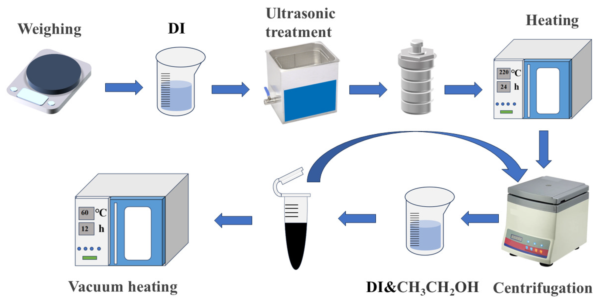
2. Experiment
3. Result and Discussion
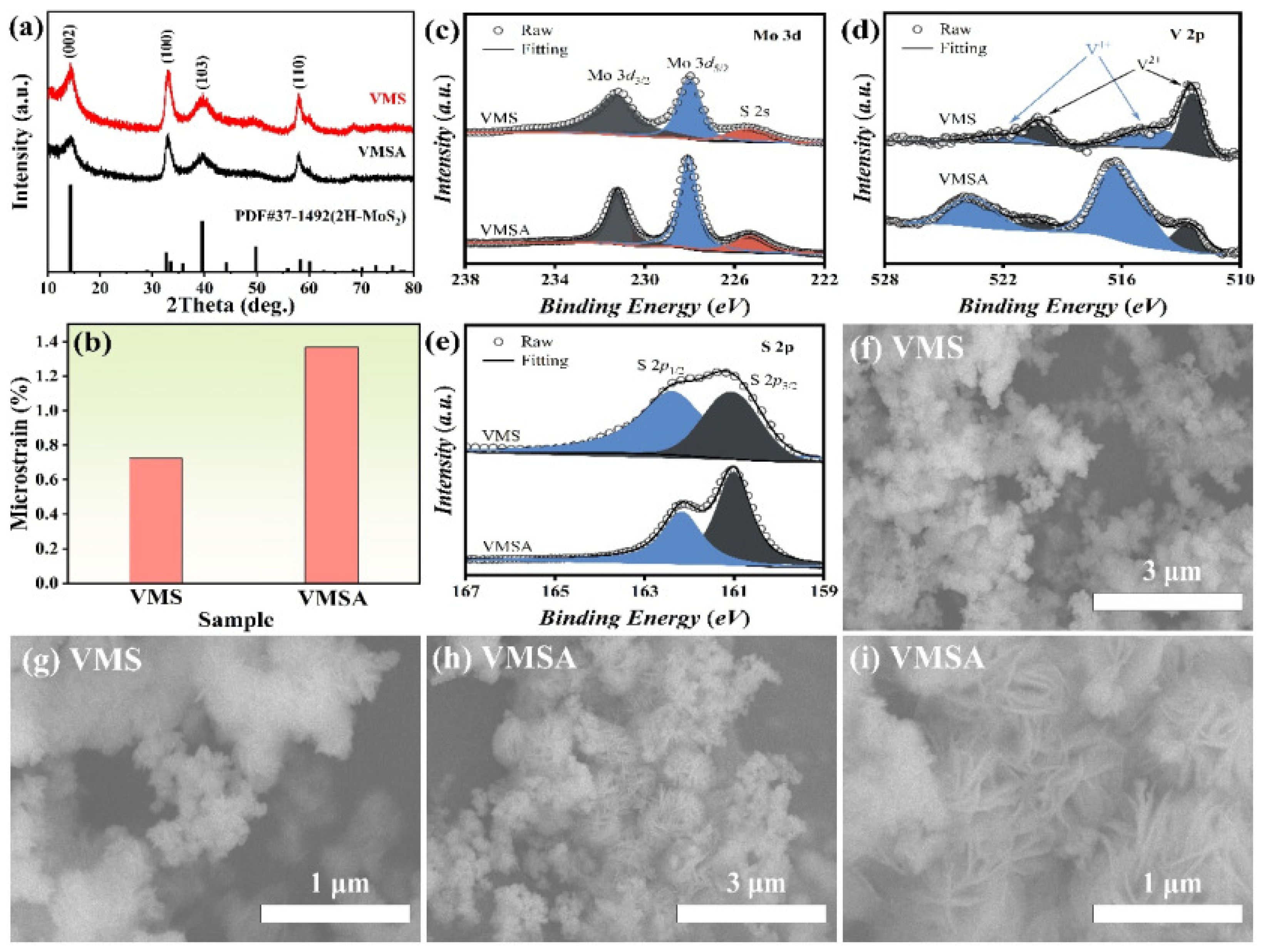
3.1. The Phase Structure and Microstructure of VMS and VMSA Materials
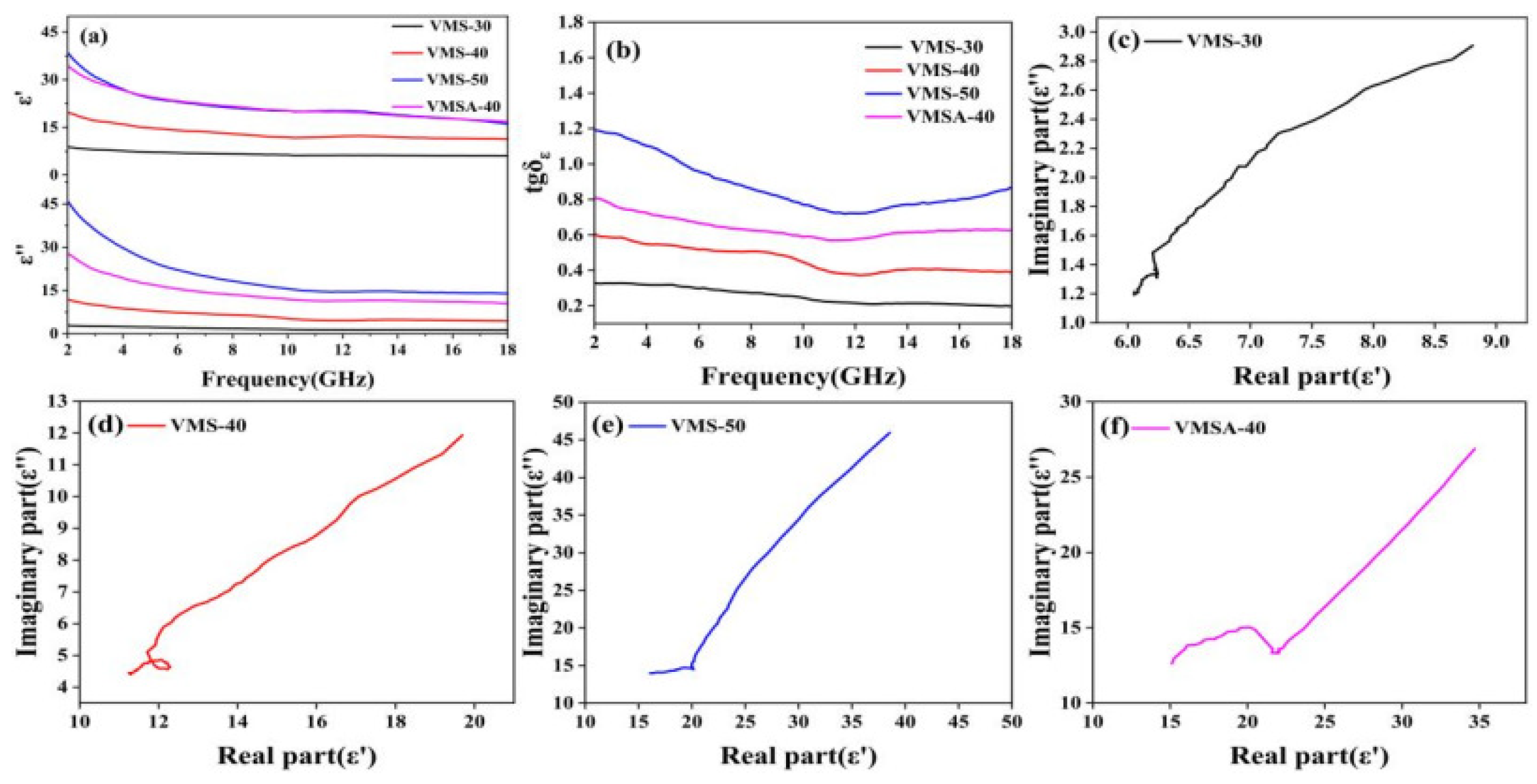
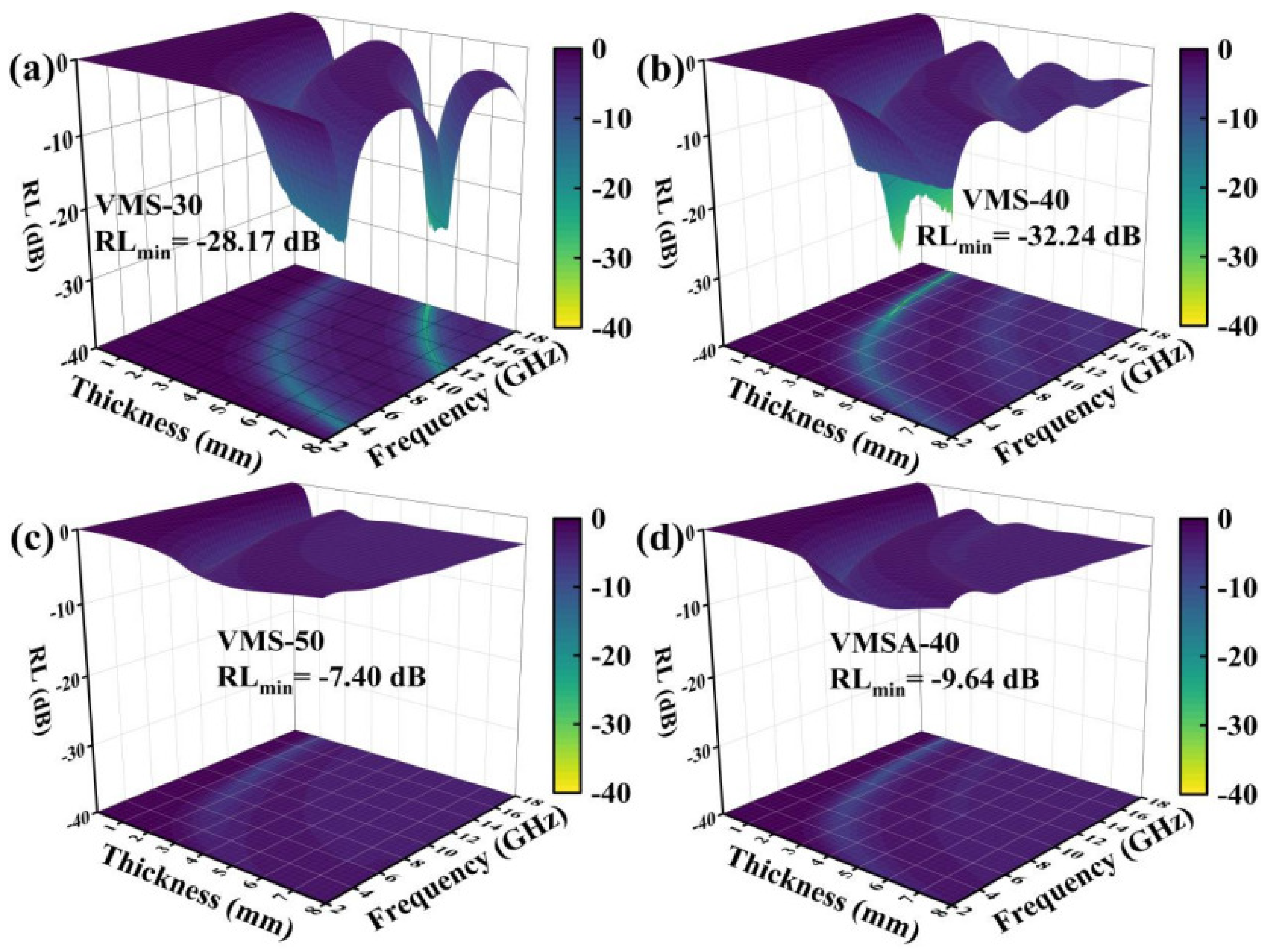
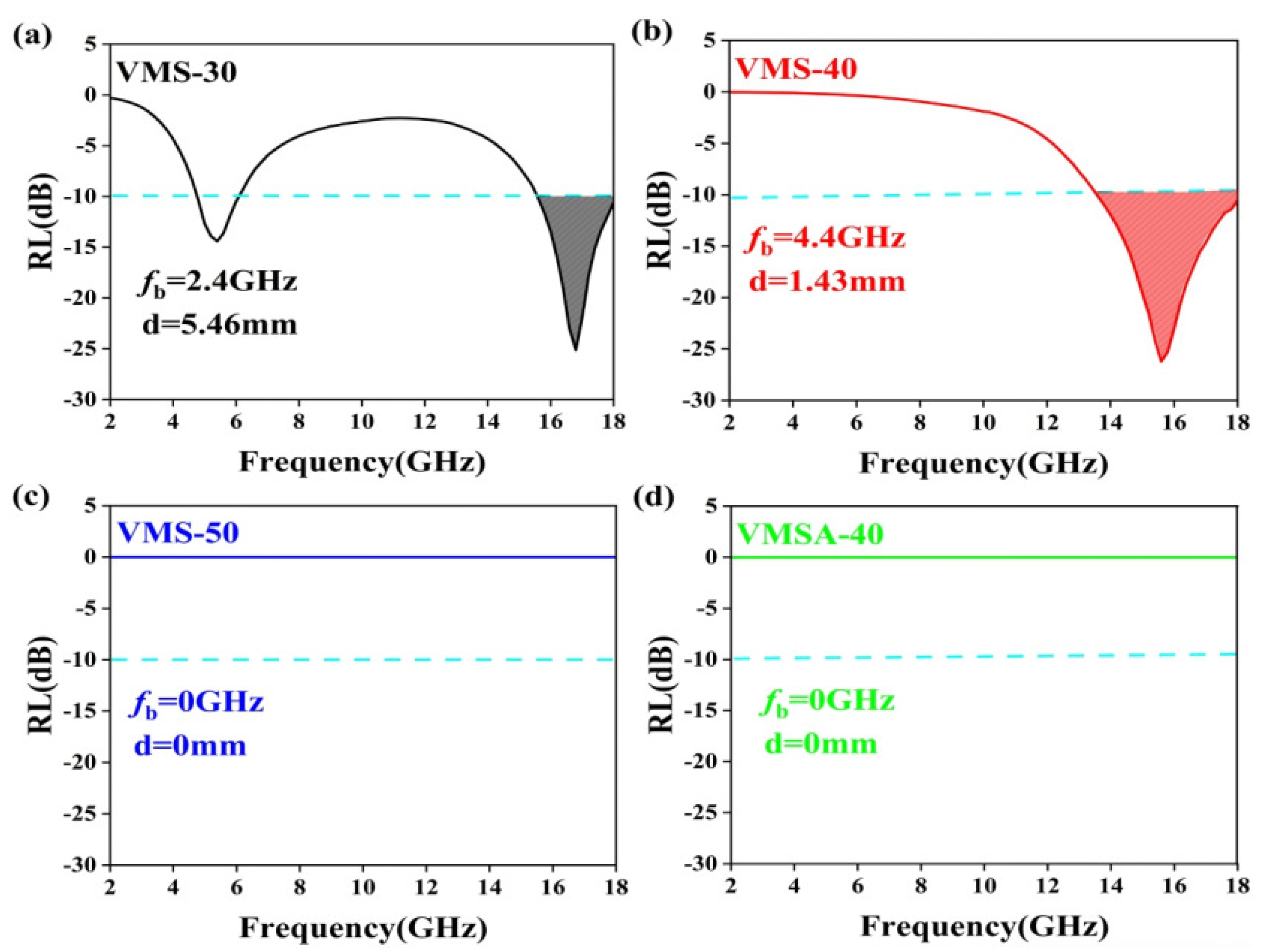
3.2. The Absorbing Properties of VMS and VMSA
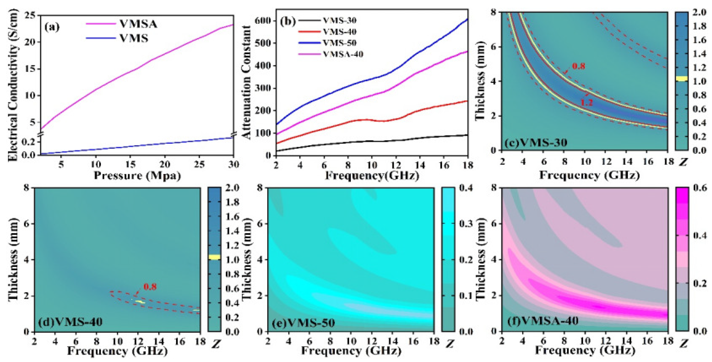
3.3. Analysis of Absorbing Mechanism
4. Conclusions
Author Contributions
Funding
Institutional Review Board Statement
Informed Consent Statement
Data Availability Statement
Conflicts of Interest
Abbreviations
| RLmin | Minimum reflection loss |
| EAB | Effective absorption bandwidth |
| EM | Electromagnetic |
| MAMs | Microwave absorbing materials |
| RL | Reflection loss |
References
- Xiao, J.; He, M.; Zhan, B.; Guo, H.; Yang, J.; Zhang, Y.; Qi, X.; Gu, J. Multifunctional microwave absorption materials: Construction strategies and functional applications. Mater. Horiz. 2024, 11, 5874–5894. [Google Scholar] [CrossRef] [PubMed]
- Siriwitpreecha, A.; Rattanadecho, P.; Wessapan, T. The influence of wave propagation mode on specific absorption rate and heat transfer in human body exposed to electromagnetic wave. Int. J. Heat Mass Transfer 2013, 65, 423–434. [Google Scholar] [CrossRef]
- Lv, H.; Yang, Z.; Wang, P.L.; Ji, G.; Song, J.; Zheng, L.; Zeng, H.; Xu, Z. A voltage-boosting strategy enabling a low-frequency, flexible electromagnetic wave absorption device. Adv. Mater. 2018, 30, 1706343. [Google Scholar] [CrossRef] [PubMed]
- Li, Q.; Zhang, Z.; Qi, L.; Liao, Q.; Kang, Z.; Zhang, Y. Toward the application of high frequency electromagnetic wave absorption by carbon nanostructures. Adv. Sci. 2019, 6, 1801057. [Google Scholar] [CrossRef]
- Xiao, J.; Zhan, B.; He, M.; Qi, X.; Zhang, Y.; Guo, H.; Qu, Y.; Zhong, W.; Gu, J. Mechanically robust and thermal insulating nanofiber elastomer for hydrophobic, corrosion-resistant, and flexible multifunctional electromagnetic wave absorbers. Adv. Funct. Mater. 2025, 35, 2419266. [Google Scholar] [CrossRef]
- Pan, J.; Sun, X.; Wang, T.; Zhu, Z.; He, Y.; Xia, W.; He, J. Porous coin-like Fe@MoS2 composite with optimized impedance matching for efficient microwave absorption. Appl. Surf. Sci. 2018, 457, 271–279. [Google Scholar] [CrossRef]
- Xiao, J.; Qi, X.; Wang, L.; Jing, T.; Yang, J.L.; Gong, X.; Chen, Y.; Qu, Y.; Peng, Q.; Zhong, W. Anion regulating endows core@shell structured hollow carbon spheres@MoSxSe2−x with tunable and boosted microwave absorption performance. Nano Res. 2023, 16, 5756–5766. [Google Scholar] [CrossRef]
- Zhang, R.; Du, Y.; Han, G.; Gao, X. Ferromagnetism and microwave absorption properties of Cr-doped MoS2 nanosheets. J. Mater. Sci. 2019, 54, 552–559. [Google Scholar] [CrossRef]
- Xiang, L.; Darboe, A.K.; Luo, Z.; Qi, X.; Shao, J.J.; Ye, X.J.; Liu, C.S.; Sun, K.; Qu, Y.; Xu, J.; et al. Constructing two-dimensional/two-dimensional reduced graphene oxide/MoX2 (X=Se and S) van der Waals heterojunctions: A combined composition modulation and interface engineering strategy for microwave absorption. Adv. Compos. Hybrid Mater. 2023, 6, 215. [Google Scholar] [CrossRef]
- Li, C.; Qi, X.; Gong, X.; Peng, Q.; Chen, Y.; Xie, R.; Zhong, W. Magnetic-dielectric synergy and interfacial engineering to design yolk-shell structured CoNi@void@C and CoNi@void@C@MoS2 nanocomposites with tunable and strong wideband microwave absorption. Nano Res. 2022, 15, 6761–6771. [Google Scholar] [CrossRef]
- Zhang, D.; Jia, Y.; Cheng, J.; Chen, S.; Chai, J.; Yang, X.; Wu, Z.; Wang, H.; Zhang, W.; Zhao, Z.; et al. High-performance microwave absorption materials based on MoS2-graphene isomorphic hetero-structures. J. Alloys Compd. 2018, 758, 62–71. [Google Scholar] [CrossRef]
- Xiao, J.; Qi, X.; Gong, X.; Peng, Q.; Chen, Y.; Xie, R.; Zhong, W. Defect and interface engineering in core@shell structure hollow carbon@MoS2 nanocomposites for boosted microwave absorption performance. Nano Res. 2022, 15, 7778–7787. [Google Scholar] [CrossRef]
- Wang, F.; Gu, W.; Chen, J.; Wu, Y.; Zhou, M.; Tang, S.; Cao, X.; Zhang, P.; Ji, G. The point defect and electronic structure of K doped LaCo0.9Fe0.1O3 perovskite with enhanced microwave absorbing ability. Nano Res. 2022, 15, 3720–3728. [Google Scholar] [CrossRef]
- Xiao, J.; Zhan, B.; Qi, X.; Ding, J.; Qu, Y.; Gong, X.; Yang, J.L.; Wang, L.; Zhong, W.; Che, R. Metal valence state modulation strategy to design core@ shell hollow carbon microspheres@MoSe2/MoOx multicomponent composites for anti-corrosion and microwave absorption. Small 2025, 21, 2311312. [Google Scholar] [CrossRef] [PubMed]
- Sapna, Budhiraja, N.; Kumar, V.; Singh, S.K. X-ray analysis of NiFe2O4 nanoparticles by Williamson-Hall and size-strain plot method. J. Adv. Phys. 2017, 6, 1–4. [Google Scholar] [CrossRef]
- Zou, J.; Cai, Z.; Lai, Y.; Tan, J.; Zhang, R.; Feng, S.; Wang, G.; Lin, J.; Liu, B.; Cheng, H.M. Doping concentration modulation in vanadium-doped monolayer molybdenum disulfide for synaptic transistors. ACS Nano 2021, 15, 7340–7347. [Google Scholar] [CrossRef] [PubMed]
- Gao, D.; Xue, Q.; Mao, X.; Wang, W.; Xu, Q.; Xue, D. Ferromagnetism in ultrathin VS2 nanosheets. J. Mater. Chem. C 2013, 1, 5909–5916. [Google Scholar] [CrossRef]
- Zhang, J.; Zhang, C.; Wang, Z.; Zhu, J.; Wen, Z.; Zhao, X.; Zhang, X.; Xu, J.; Lu, Z. Synergistic interlayer and defect engineering in VS2 nanosheets toward efficient electrocatalytic hydrogen evolution reaction. Small 2018, 14, 1703098. [Google Scholar] [CrossRef]
- Dai, X.; Du, K.; Li, Z.; Sun, H.; Yang, Y.; Zhang, W.; Zhang, X. Enhanced hydrogen evolution reaction on few–layer MoS2 nanosheets–coated functionalized carbon nanotubes. Int. J. Hydrogen Energy 2015, 40, 8877–8888. [Google Scholar] [CrossRef]
- Pan, H.; Xu, L.; Li, K.; Li, T.; Shen, Y.; Wang, L. The electromagnetic wave absorption composite of flower-like structure NiCo2O4 and Fe3O4 derived from low-temperature preparation method. Mater. Sci. Eng. B 2023, 296, 116714. [Google Scholar] [CrossRef]
- Sun, X.; He, J.; Li, G.; Tang, J.; Wang, T.; Guo, Y.; Xue, H. Laminated magnetic graphene with enhanced electromagnetic wave absorption properties. J. Mater. Chem. C 2013, 1, 765–777. [Google Scholar] [CrossRef]
- Zhao, H.; Seow, J.Z.Y.; Cheng, Y.; Xu, Z.J.; Ji, G. Green synthesis of hierarchically porous carbons with tunable dielectric response for microwave absorption. Ceram. Int. 2020, 46, 15447–15455. [Google Scholar] [CrossRef]
- Upadhyay, B.; Sharma, R.; Maity, D.; Narayan, T.N.; Pal, S.K. Ultrafast carrier dynamics in vanadium-doped MoS2 alloys. Nanoscale 2023, 15, 16344–16353. [Google Scholar] [CrossRef] [PubMed]
- Luo, C.; Tang, Y.; Jiao, T.; Kong, J. High-temperature stable and metal-free electromagnetic wave- absorbing SiBCN ceramics derived from carbon-rich hyperbranched polyborosilazanes. ACS Appl. Mater. Interfaces 2018, 10, 28051–28061. [Google Scholar] [CrossRef]
- Wu, C.; Wang, J.; Zhang, X.; Kang, L.; Cao, X.; Zhang, Y.; Niu, Y.; Yu, Y.; Fu, H.; Shen, Z.; et al. Hollow gradient-structured iron-anchored carbon nanospheres for enhanced electromagnetic wave absorption. Nano-Micro Lett. 2022, 15, 7–23. [Google Scholar] [CrossRef]
- Fan, G.; Jiang, Y.; Xin, J.; Zhang, Z.; Fu, X.; Xie, P.; Cheng, C.; Liu, Y.; Qu, Y.; Sun, K.; et al. Facile synthesis of Fe@Fe3C/C nanocomposites derived from bulrush for excellent electromagnetic wave-absorbing properties. ACS Sustain. Chem. Eng. 2019, 7, 18765–18774. [Google Scholar] [CrossRef]
- Liao, Q.; He, M.; Zhou, Y.; Nie, S.; Wang, Y.; Wang, B.; Yang, X.; Bu, X.; Wang, R. Rational construction of Ti3C2Tx/Co-MOF-derived laminated Co/TiO2-C hybrids for enhanced electromagnetic wave absorption. Langmuir 2018, 34, 15854–15863. [Google Scholar] [CrossRef]
- Yang, H.; Zhang, X.; Xiong, Z.; Shen, Z.; Liu, C.; Xie, Y. Cu2O@ nanoporous carbon composites derived from Cu- based MOFs with ultrabroad-bandwidth electromagnetic wave absorbing performance. Ceram. Int. 2021, 47, 2155–2164. [Google Scholar] [CrossRef]
- Wang, X.; Xing, X.; Zhu, H.; Li, J.; Liu, T. State of the art and prospects of Fe3O4/carbon microwave absorbing composites from the dimension and structure perspective. Adv. Colloid Interface Sci. 2023, 318, 102960. [Google Scholar] [CrossRef]
- Lan, X.; Li, Y.; Wang, Z. High-temperature electromagnetic wave absorption, mechanicaland thermal insulation properties of in-situ grown SiC on porous SiC skeleton. Chem. Eng. J. 2020, 397, 125250. [Google Scholar] [CrossRef]
- Zhao, T.; Jia, Z.; Zhang, Y.; Wu, G. Multiphase molybdenum carbide doped carbon hollow sphere engineering: The superiority of unique double-shell structure in microwave absorption. Small 2023, 19, 2206323. [Google Scholar] [CrossRef] [PubMed]
- Li, T.; Zhi, D.; Chen, Y.; Li, B.; Zhou, Z.; Meng, F. Multiaxial electrospun generation of hollow graphene aerogel spheres for broadband high-performance microwave absorption. Nano Res. 2020, 13, 477–484. [Google Scholar] [CrossRef]
- Wang, H.; Meng, F.; Li, J.; Li, T.; Chen, Z.; Luo, H.; Zhou, Z. Carbonized design of hierarchical porous carbon/Fe3O4@Fe derived from loofah sponge to achieve tunable high-performance microwave absorption. ACS Sustain. Chem. Eng. 2018, 6, 11801–11810. [Google Scholar] [CrossRef]
- Li, G.; Wang, L.; Li, W.; Ding, R.; Xu, Y. CoFe2O4 and/or Co3Fe7 loaded porous activated carbonballs as a lightweight microwave absorbent. Phys. Chem. Chem. Phys. 2014, 16, 12385–12392. [Google Scholar] [CrossRef] [PubMed]
- Wang, T.; Chen, G.; Zhu, J.; Gong, H.; Zhang, L.; Wu, H. Deep understanding of impedance matching and quarter wavelength theory in electromagnetic wave absorption. J. Colloid Interface Sci. 2021, 595, 1–5. [Google Scholar] [CrossRef]
- Li, Y.; Zhao, Y.; Lu, X.; Zhu, Y.; Jiang, L. Self-healing superhydrophobic polyvinylidene fluoride/Fe3O4@polypyrrole fiber with core–sheath structures for superior microwave absorption. Nano Res. 2016, 9, 2034–2045. [Google Scholar] [CrossRef]
- Liu, W.; Shao, Q.; Ji, G.; Liang, X.; Cheng, Y.; Quan, B.; Du, Y. Metal–organic-frameworks derived porous carbon-wrapped Ni composites with optimized impedance matching as excellent lightweight electromagnetic wave absorber. Chem. Eng. J. 2017, 313, 734–744. [Google Scholar] [CrossRef]

| Sample | RLmin (dB) | d (mm) | f (GHz) | Bandwidth (GHz) | EAB (GHz) | d (mm) | RL (dB) | f (GHz) |
|---|---|---|---|---|---|---|---|---|
| VMS-30 | −28.17 | 5.10 | 18.00 | 1.27 | 2.40 | 5.46 | −25.09 | 16.81 |
| VMS-40 | −32.24 | 1.78 | 12.20 | 3.23 | 4.40 | 1.43 | −26.22 | 15.60 |
| VMS-50 | −7.40 | 1.38 | 11.60 | 0.00 | 0.00 | 0.00 | 0.00 | 0.00 |
| VMSA-40 | −9.64 | 1.45 | 11.40 | 0.00 | 0.00 | 0.00 | 0.00 | 0.00 |
Disclaimer/Publisher’s Note: The statements, opinions and data contained in all publications are solely those of the individual author(s) and contributor(s) and not of MDPI and/or the editor(s). MDPI and/or the editor(s) disclaim responsibility for any injury to people or property resulting from any ideas, methods, instructions or products referred to in the content. |
© 2025 by the authors. Licensee MDPI, Basel, Switzerland. This article is an open access article distributed under the terms and conditions of the Creative Commons Attribution (CC BY) license (https://creativecommons.org/licenses/by/4.0/).
Share and Cite
Zou, J.; Xie, Q. Study on the Absorbing Properties of V-Doped MoS2. Ceramics 2025, 8, 84. https://doi.org/10.3390/ceramics8030084
Zou J, Xie Q. Study on the Absorbing Properties of V-Doped MoS2. Ceramics. 2025; 8(3):84. https://doi.org/10.3390/ceramics8030084
Chicago/Turabian StyleZou, Jiang, and Quan Xie. 2025. "Study on the Absorbing Properties of V-Doped MoS2" Ceramics 8, no. 3: 84. https://doi.org/10.3390/ceramics8030084
APA StyleZou, J., & Xie, Q. (2025). Study on the Absorbing Properties of V-Doped MoS2. Ceramics, 8(3), 84. https://doi.org/10.3390/ceramics8030084