Article

Improving the Quality of Ceramic Products by Removing the Defective Surface Layer

Department of High-Efficiency Processing Technologies, Moscow State University of Technology “STANKIN”, Vadkovskiy per. 3A, 127055 Moscow, Russia
*
Author to whom correspondence should be addressed.
Ceramics 2024, 7(1), 55-67; https://doi.org/10.3390/ceramics7010005
Submission received: 6 October 2023 / Revised: 1 December 2023 / Accepted: 9 January 2024 / Published: 11 January 2024

Abstract

:
The surface of ceramic products manufactured using diamond grinding is replete with shallow scratches, deep grooves and other defects. The thickness of the defective layer amounts to 3–4 µm and it must be removed to increase wear resistance of the products when exposed to intense thermomechanical loads. In this study, removal of the defective layers from samples made of ZrO2, Al2O3 and Si3N4 with a beam of fast argon atoms was carried out with a stripping rate of up to 5 µm/h. To prevent contamination of the source of fast argon atoms by the sputtered dielectric material, the beam was compressed and passed to the sample through a small hole in a wide screen. Due to the removal of the defective layer, abrasive wear decreased by an order of magnitude and the adhesion of coatings deposited on the cleaned ceramic surfaces improved significantly.

1. Introduction

In the past decade, the share of ceramic materials used in the manufacturing of the most important engineering products—bearing parts and automotive components, elements of aircraft engines, rocket and space technology, drawing and cutting tools—has increased significantly. This is due to success in the development of ceramic materials, obtaining high-quality initial powders, the possibility of choosing the best compositions of powders, the emergence of new sintering technologies and the optimization of their key parameters, which ensure the production of ceramic blanks that are distinguished by a high density, hardness, heat resistance and low intensity of the adhesive setting with most structural steels and alloys [1,2,3].
However, the spread of ceramic materials in industry is hindered by the insufficient reliability of the ceramic parts (large scatter of mean time between failures). This drawback is especially pronounced when combined with increased thermal and mechanical loads, as well as when the ceramic surface is exposed to cyclic loads. With such a nature of operational loads, the loss of the working state of ceramic parts can occur at various stages of their operation—both during the running-in period and at the stage of stable wear. This is due to a number of reasons—the inhomogeneity of the structure of ceramic materials inherent in their nature, and technological defects present in the surface layer of ceramic parts, which can be formed in the process of diamond grinding (shaping) of sintered ceramic blanks.
With a complex thermomechanical effect on a ceramic workpiece during diamond grinding, the removal of the surface layer to the required depth occurs as a result of creating stresses in it, the level of which exceeds the material fracture stress. After grinding, a characteristic stress state is formed in the surface layer of ceramic products—significant compressive stresses are observed on the surface [4,5], after which the stresses sharply decrease and are replaced by tensile stresses, which then gradually decrease and stabilize already at depth. In addition, as a result of the impact action of diamond grains, as well as the local plastic deformation that occurs during high-speed heating of the surface areas of ceramics and their rapid cooling, the surface of ceramic parts has a specific relief, including a set of defects—grooves with longitudinal cracks, tearing of single grains and their conglomerates, microprotrusions, etc.
These defects are stress concentrators, which, when exposed to intense thermomechanical loads during operation, lead to accelerated micro- and macro-destruction of contact surfaces, which reduces the wear resistance of ceramic parts and hinders the use of promising ceramic materials in mechanical engineering. Therefore, increasing the wear resistance of the surface layer of ceramic parts under the influence of increased thermomechanical loads is currently an urgent task that requires the development of new scientifically based technological approaches and solutions.
An obvious solution for increasing the wear resistance of the surface layer of ceramic parts could be deposition of wear-resistant coatings, such as TiAlN, CrAlN, TiZrN, TiCN, DLC, etc. The application of these nitride and diamond-like coatings to metallic parts due to an increase in microhardness and a decrease in frictional and adhesive interaction on the contact pads makes it possible to ensure high operational stability and increase wear resistance by an average of three times [6,7]. At the same time, the application of similar coatings to ceramic parts demonstrates a maximum achieved effect of about 1.6–1.8 times for oxide–carbide ceramics.
Obviously, the impossibility of fully realizing the potential of wear-resistant coatings deposited on ceramic parts is mainly due to the defective state of the surface that occurs after diamond grinding. High efficiency cannot be expected from a thin coating deposited on a defective layer. Previously, it was believed that the coating was able to “heal” surface defects by filling them [8]. Practice shows that a coating with a thickness of not more than 4 µm (a coating of greater thickness flakes off from ceramic samples) is only able to partially level surface defects—it is able to fill in small scratches or grain chips, but does not allow leveling deep grooves and filling voids from torn grains [9].
To eliminate or minimize the presence of a defective layer, precision finishing or polishing could be used. This would create a favorable basis for the coating’s formation. Of course, before the precision finishing, the surface roughing is needed—stripping of the defective layer with a thickness of 2–4 µm.
For removing the surface layer of a part, the chemical method based on the use of various acid solutions is widely used. The part is placed in acid to dissolve the surface layer. The use of hazardous chemicals imposes additional safety precautions and increases the risk of industrial accidents. The disposal of used solutions is one of the main problems of this method. Chemically stripped samples may have a roughness similar to that of the initial material [10,11]. The disadvantages of chemical methods are long stripping times and large volumes of toxic waste [12]. These problems can be resolved using electrochemical dissolution, which is both faster and safer for the environment [13].
For rapid and high-quality removal of the surface layer, a pulsed laser beam can be used. Laser stripping is a more ecologically friendly, effective method [14]. However, the laser removal of the surface layer demonstrates a quite uneven surface of treated samples. One of the reasons is a small value of the laser spot diameter, ~0.1 mm. Melting and evaporation at subsequent points of the sample result in a wavy surface with a wave length comparable with the laser spot diameter. To avoid this, acting on the surface with a broad beam of uniformly distributed particles is needed. The particles might be accelerated ions or fast neutral atoms.
There exist a lot of ion sources, which produce beams with circular cross-sections [15]. The beam diameter can amount to 38 cm [16] or even reach 50 cm [17]. The plasma emitter of ions is produced in a gas discharge chamber with thermionic cathodes. Ions are accelerated from the emitter by an ion optical system consisting of two or three parallel grids. The ion beam current can reach several amperes at the ion energy up to several keV.
The sources with thermionic cathodes cannot produce ions of reactive gases. Therefore, ion sources with plasma emitters generated in a gas discharge with a cold hollow cathode were developed [18,19]. As the positive ions are able to charge the surface of any samples under processing and sometimes provoke undesirable defects in the superficial layer, it is reasonable to use sources of fast neutral atoms [20,21,22] instead of ion sources.
The fast neutral atoms appear due to charge exchange collisions of accelerated ions with gas atoms. For instance, at room temperature and a gas pressure of p = 0.2 Pa, the mean free path λ of argon atoms is equal to 0.04 m [23]. And the mean free path λc of argon ions between charge exchange collisions amounts to ~0.1 m at the ion energy from 0.5 to 6 keV [24,25]. It means that the number of elastic collisions between argon atoms exceeds the number of their charge exchange collisions with accelerated ions by two or three times. However, this does not prevent fast atoms from efficiently sputtering the sample at a rate proportional to their energy and flux density on the sample surface. The sputtering rate is an important parameter that determines the applicability of fast atoms for the defective layer removal.
From a practical point of view, the processing time should not exceed the time of ~10–20 min needed to evacuate a working vacuum chamber after loading the sample therein. Therefore, to remove the defective layer with a thickness of 3 μm within 20 min, the etching rate should be about 10 μm/h.
Another important factor is the reliability of the source of fast argon atoms at high etching rates of dielectric materials. When removing a 3-μm-thick surface layer from a dielectric ceramic sample with an area comparable with that of the accelerating grid of the beam source, the flow of sputtered dielectric material is moving toward the grid. Deposition of dielectric films on the grid and other electrodes causes electric breakdowns and failure of the beam source. In this work, a new type of fast-atom beam source was proposed, which made it possible to protect the electrodes of the source from impurities and prevent electrical breakdowns. This made it possible to remove fairly thick defective layers from dielectric ceramic samples and to study the effect of the removal on characteristics of the sample surface and wear-resistant coatings applied to it.

2. Materials and Methods

2.1. Experimental Setup

To conduct experiments on the removal of a defective surface layer, rectangular samples were produced from sintered ceramic blanks (based on ZrO2, Al2O3 and Si3N4) subjected to diamond grinding. The sample length and width were equal to 16 mm and their thickness amounted to 8 mm. They were processed using a setup presented in Figure 1.
The setup comprises a 50-cm-high, 40-cm-wide and 30-cm-long rectangular vacuum chamber equipped with a beam source of fast argon atoms. Inside a grounded cylindrical housing of the beam source is mounted a 30-cm-diameter and 25-cm-long hollow cathode. Its output orifice is covered with a 20-cm-diameter concave grid. The radius of the grid surface curvature amounts to 20 cm.
Positive poles of a gas discharge power supply and an accelerating voltage power supply are connected to an anode mounted inside the hollow cathode. The negative pole of the gas discharge power supply is connected to the hollow cathode and the negative pole of the accelerating voltage power supply is connected to the grid. Through a resistor, the grid is connected to the vacuum chamber.
Opposite the grid is a screen passing through the focal point of the grid. The screen is made of a 1-mm-thick titanium sheet and has a 1-cm-diameter hole in the center. It is attached to the housing of the beam source where the hole is located in the focal area of the grid. At a distance of 15 cm from the screen is positioned a holder of the samples. It can hold up to seven samples facing the screen and arranged vertically. The holder is attached to a removable flange at the top of the chamber for loading samples into it. The samples are fixed on the holder outside the chamber, then the flange is installed in place and the chamber is evacuated.
The working gas is injected into the hollow cathode. Through the hole of the screen, it passes into the working vacuum chamber and is pumped out from the chamber through a 20-cm-diameter pumping channel on the opposite wall of the chamber.
On the left and right walls of the chamber, there are two magnetron targets made of titanium diboride. The height of the targets is equal to 16 cm and their width is equal to 8 cm.
A quartz window on the top of the chamber allows in situ measuring of the temperature of the samples with an infrared pyrometer. There is a sliding shutter that prevents deposition of metal films on the window. A solenoid is installed outside the housing of the beam source to create inside the hollow cathode an axial magnetic field.
When at the gas pressure of 0.2 Pa, the discharge power supply and the accelerating voltage power supply are switched on, and the hollow cathode is filled with a glow discharge plasma. Ions accelerated between the plasma and the grid fly through the grid holes toward the screen. Their energy is defined with the difference between the potential of plasma filling the hollow cathode, which is equal to the accelerating voltage U, and the potential of plasma filling the chamber, which is close to the chamber potential. Hence, the energy of ions passed through the grid amounts to Ei = eU, where e is the electron charge. When colliding with gas atoms, accelerated ions transfer to them electrical charges and turn into fast neutral atoms without changing their energy and direction of movement. Charge exchange collisions result in the appearance of slow ions. Neutralization of their charges by electrons emitted by the chamber and the screen leads to the formation of a secondary plasma on both sides of the screen.
The slow ions move to the chamber walls and the screen connected to the chamber. Their current through the resistor induces a negative voltage of 100–200 V on the grid, thus preventing electrons of the secondary plasma from entering the hollow cathode of the beam source.
Taking into account that at a pressure of 0.2 Pa, the gas density is equal to no = 5 × 10¹⁹ m−3 [23] and the charge exchange collision cross-section of argon ions with 4 keV energy is equal to σc = 2 × 10⁻¹⁹ m2 [24,25], we obtain for the mean free path of argon ions between the charge exchange collisions λc = 1/noσc = 0.1 m. Since the distance of 0.2 m between the grid and the screen hole is two times greater, we may believe that most of the ions that passed through the screen hole are already converted into fast argon atoms.
The inner surface area of the hollow cathode is Sc = 4500 cm2 and at a current of Ic = 2 A in the cathode circuit, the ion current density on its surface is equal to ji = Ic/Sc = 2000/4500 = 0.44 mA/cm2. Taking into account a high plasma homogeneity in the hollow cathode glow discharge [26], we may believe that the current density of ions accelerated from the plasma toward the grid has the same value. At the grid surface area of Sg = 850 cm2 and transparency of η = 0.75, the current of accelerated ions moving from the grid toward the screen hole is equal to η ji Sg = 0.28 A. The power transported by fast argon atoms with an energy of 4 keV is 0.28 × 4 = 1.12 kW.
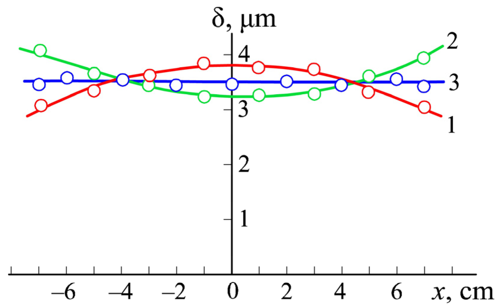
To determine the distribution along the sample holder of the etching rate by fast atoms, a 16-cm-long, 2-cm-wide and 2-mm-thick titanium target was vertically fastened to the holder. The target surface facing the screen was polished and covered with a 16-cm-long, 1-cm-wide and 1-mm-thick titanium mask. After a 1-h-long etching with 4 kV argon atoms, the titanium target was taken from the chamber and the mask was removed from its surface. Using a Dektak XT stylus profilometer by Bruker Nano, Inc. (Billerica, MA, USA), the height of the step between the target surface covered with the mask and its open surface subjected to etching with fast argon atoms was measured. Line 1 in Figure 2 presents dependence of the step height δ on the distance x from the target center. It shows that δ is the maximum at the center of the target at x = 0 and is decreasing at the ends of the target at x = −8 cm and x = 8 cm. The reason for the unevenness of the etching rate may be an increase in the angle of incidence of fast argon atoms arriving at the target from the screen hole with increasing distance x to the target center (see Figure 1).
The flux density distribution of fast atoms became more uniform in the presence of the magnetic field in the hollow cathode. Before installing on the setup, at a direct current of Is = 1 A through the solenoid, the maximum magnetic inductance on its axis was measured using a teslameter PIE.MG R-2 (Mayak-2M) produced by ZAPADPRIBOR LLC, Moscow, Russia. It was found to be equal to 0.002 T. Line 2 in Figure 2 shows the distribution of the step height δ on another target etched with 4 kV argon atoms for 1 h at the hollow cathode current of Ic = 2 A and the solenoid current of Is = 3 A. It shows that in this case, the maximum step height δ is shifted to the ends of the target.
It is due to the magnetic field action on the electrons emitted by the cylindrical surface of the hollow cathode. After acceleration in the cathode sheath to the energy Ee = eUc, where Uc ~ 400 V is the cathode fall of potential, they are deflected in the magnetic field and forced to return to the cathode sheath. In the sheath, electrons are reflected to plasma and then again return to the sheath. The maximum distance of the electrons from the cathode surface amounts to their Larmor radius, RL = (2mε)1/2/eB, where m and e are the mass and charge of electrons, ε is their energy and B is the induction of the magnetic field. When the energy is measured in eV, then RL(m) = 3.37 × 10⁻⁶ [ε(eV)]1/2/B(T).
For instance, at the solenoid current of Is = 3 A, the induction B = 0.006 T and ε = 400 eV, the RL = 1.12 cm. The electrons emitted by the cylindrical surface of the hollow cathode are confined in the 1.12-cm-thick layer adjacent to this surface. This increases the ionization intensity in this layer, the current density of accelerated ions at the periphery of the grid and the etching intensity at the ends of the target. Reducing the solenoid current to Is = 1.7 A led to a fairly uniform etching of the target (line 3 in Figure 2).
Thus, the developed source of fast argon atoms, equipped with a screen that prevents the deposition of sputtered dielectric material on its accelerating grid, ensures fairly uniform etching of samples with a diameter comparable to the diameter of the grid. The sputtering rate of the titanium target is 3.5 µm/h at a distance of 15 cm between the sample holder and the screen. Reducing the distance to 7.5 cm should increase the etching rate to 14 µm/h. Thus, this source is suitable for removing defective surface layers from dielectric ceramic samples.

2.2. Characterization of the Samples

A Calotest instrument produced by CSM Instruments (Alpnach, Switzerland) was used for characterization of the abrasion resistance of the ceramic samples.
For in situ measuring of the sample temperature, an infrared pyrometer, IMPAC IP 140 (LumaSense Technologies GmbH, Frankfurt am Main, Germany), was used.
Characterization of the coating adhesion was performed using a Nanovea M1 Hardness and Scratch Tester produced by Nanovea Inc. (Irvine, CA, USA).
The elemental analysis of sample material was provided by a VEGA3 LMH scanning electron microscope (Tescan, Brno, Czech Republic).
The profilograms of the sample surface were obtained using the HOMMEL TESTER T8000 high-precision profilograph–profilometer produced by the company Hommelwerke GmbH (JENOPTIK Industrial Metrology Germany GmbH, Jena, Germany).
The roughness of the sample surface was evaluated using a Dektak XT stylus profilometer manufactured by Bruker Nano, Inc. (Billerica, MA, USA).

3. Results

3.1. Removal of Defective Surface Layer

Before experiments, every sample was ultrasonically cleaned in acetone. Using a profilometer Dektak XT, the roughness of the sample surface was measured. Figure 3 presents profilograms of the manufactured samples of three dielectric ceramics: silicon nitride, zirconium oxide and aluminum oxide.
To measure the thickness of the surface layer removed from the sample by fast argon atoms, a part of the sample surface was covered with a mask before treatment. The mask was a 5-mm-wide titanium strip pressing the sample to the holder with two screws. After a silicon nitride sample with a mask was fastened in the middle of the holder, the vacuum chamber was pumped down and argon was introduced to the hollow cathode, thus increasing the gas pressure to 0.2 Pa.
Having turned on the power supplies, a current in the hollow cathode circuit of Ic = 2 A, an accelerating voltage of U = 4 kV and a solenoid current of Is = 1.7 A were established. This led to the appearance of a faint glow of secondary plasma in the chamber, visible through the quartz window. The window made it possible to measure the sample temperature using an infrared pyrometer. A total of 10 min after turning on the source of fast argon atoms, the sample temperature increased to 450 °C. After etching the sample for 1 h, it was cooled in a vacuum and removed from the chamber. The height of the step between the sample surface covered with the mask and its open surface measured with the Dektak XT stylus profilometer was equal to 1.6 µm. Hence, the sample etching rate amounted to 1.6 µm/h. When an aluminum oxide sample with a mask was fastened in the middle of the holder and etched for 1 h with fast argon atoms at the same current in the hollow cathode circuit of Ic = 2 A, accelerating voltage U = 4 kV and solenoid current Is = 1.7 A, measurements yielded the etching rate of 2.3 µm/h. When a zirconium dioxide sample was treated, the etching rate amounted to 3 µm/h.
After etching the ceramic samples for 1 h, their surface roughness decreased only slightly: from Ra = 0.105 µm to Ra = 0.095 µm for Si3N4 and from Ra = 0.122 µm to Ra = 0.114 µm for ZrO2 (see Table 1).
A more noticeable decrease from Ra = 0.304 µm to Ra = 0.252 µm was observed for Al2O3. This can be explained by the approximately three times greater initial roughness of the Al2O3 sample compared to the ZrO2 and Si3N4 samples.
When polishing any material with a beam of ions or fast neutral atoms, the rate of the decrease in roughness falls down as the magnitude of the roughness diminishes. Therefore, it takes too much time to achieve a record low roughness of Ra ~ 0.001 µm. The rate of decrease in roughness for the Al2O3 sample would be close to that of ZrO2 and Si3N4 samples when its roughness would be close to their roughness of Ra ~ 0.1 µm.
Despite a long time taken to treat the dielectric samples, no failure of the fast atom source occurred. This is due to protection of the accelerating grid with a screen, preventing deposition of dielectric films and electrical breakdowns on its surface.

3.2. Deposition of Wear-Resistant Coatings

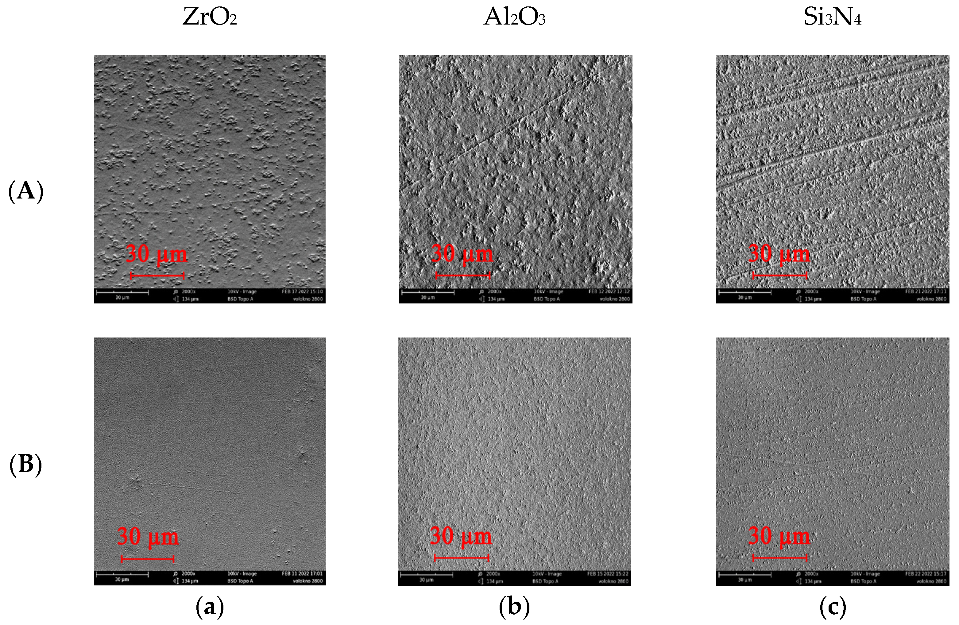
After attaching the second zirconium dioxide sample and its mask to the holder, they were first cleaned with fast argon atoms for 5 min. During the cleaning process, the sample was heated by fast argon atoms to 400 °C. Then, the magnetron power supplies were turned on, the current in the hollow cathode circuit was reduced to Ic = 0.5 A and the accelerating voltage was reduced to U = 1 kV. At stabilized currents of 2 A in the circuits of both magnetron targets, a TiB2 wear-resistant coating was deposited on the silicon nitride sample for 1 h. During the deposition process, the growing coating was continuously bombarded by fast atoms with an energy of 1 keV. When removing the sample from the chamber and removing the mask from its surface, measuring the height of the step between the masked and coated areas of the surface gave a step height of δ = 2.5 μm and a coating deposition rate of 2.5 μm/h. Since the original surface of the sample is replete with defects, a coating thickness of 2.5 µm is not enough to level them out (Figure 4(Aa)).
The third zirconium dioxide sample was subjected to combined treatment. First, it was etched for 2 h with fast argon atoms at the current in the cathode circuit of Ic = 2 A and the accelerating voltage of U = 4 kV. Immediately after etching, a wear-resistant TiB2 coating was applied to the zirconia sample for 1 h. As the thickness of the stripped surface layer of 6 µm exceeds that of the defective layer ~2–4 µm, no defects can be seen on the coated surface (Figure 4(Ba)).
The samples made of Al2O3 and Si3N4 ceramics were subjected to the same treatment. First, they were etched for 2 h with fast argon atoms at the current in the cathode circuit of Ic = 2 A and the accelerating voltage of U = 4 kV. Immediately after etching, a wear-resistant TiB2 coating was applied to the samples for 1 h. As appreciation for the thickness of the surface layers removed for 2 h from Al2O3 and Si3N4 gives, respectively, 1.6 × 2 = 3.2 µm and 2.3 × 2 = 4.6 µm, no appreciable defects are seen on SEM images of samples coated with TiB2 after removal of the surface layers.

3.3. Abrasion Resistance and Wear of Ceramic Samples

For characterization of the sample’s abrasion resistance, a Calotest instrument was used. Figure 5 shows dependencies of the abrasion volume V on the test time t for three ceramic materials.
A rotating ball was placed on the sample with a load of 0.2 N and into the contact zone an abrasive suspension was fed. Abrasive particles in the contact zone and applied external force led to local abrasion of the sample surface. The rotating ball produces on the sample surface a spherical wear notch. The notch diameter D was measured using an optical microscope. When D is much smaller than the ball radius R, the volume of worn material is equal to V = π∙D4/64R.
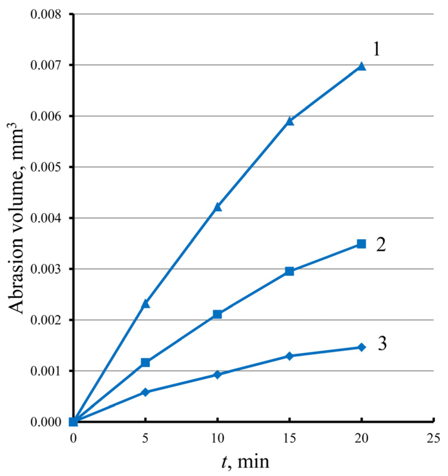
Figure 6 presents dependencies on the test time of the abrasion volume for zirconium dioxide samples before treatment (1), after deposition of 2.5-µm-thick TiB2 coating (2) and a sample coated with TiB2 after removal from it of a 6-μm-thick surface layer (3). They demonstrate that due to removal of the defective layer and deposition of wear-resistant coating, the abrasive wear diminished by an order of magnitude.
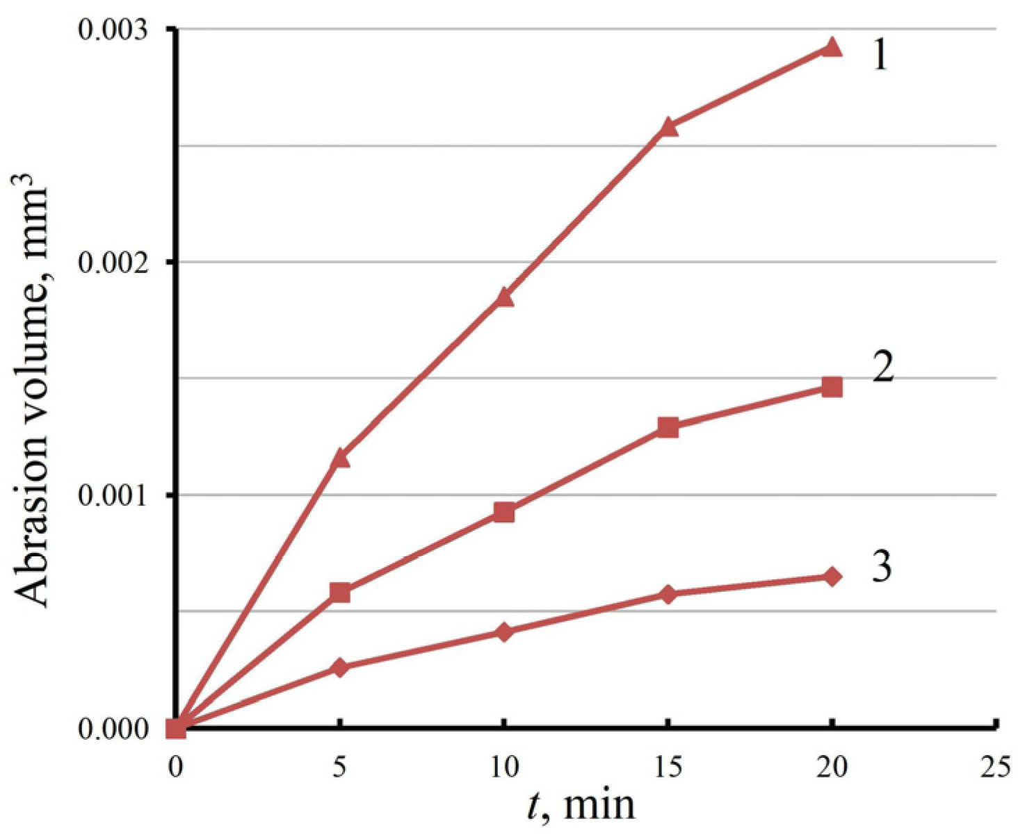
Figure 7 presents dependencies on the test time of the abrasion volume for aluminum oxide samples before treatment (1), after deposition of 2.5-µm-thick TiB2 coating (2) and a sample coated with TiB2 after removal of the defective surface layer (3). They show that due to the layer removal and wear-resistant coating deposition, the abrasive wear diminished significantly.
Figure 8 shows dependencies on the test time of the abrasion volume for silicon nitride samples before treatment (1), after deposition of 2.5-µm-thick TiB2 coating (2) and a sample coated with TiB2 after removal of the 3.2-μm-thick surface layer (3).
They show that due to removal of the defective layer and deposition of wear-resistant coating, the abrasive wear diminished significantly.
The coating adhesion was evaluated using a Nanovea M1 Hardness and Scratch Tester. The first critical load leading to first cracks on the TiB2 coating and appearance of acoustic emission was equal to Lc1 = 14 N for the Si3N4 sample coated without stripping its defective surface layer. For the Si3N4 sample coated with TiB2 after removal from its surface of the defective layer by argon atoms with an energy of 4 keV, it amounted to Lc1 = 27 N. The adhesion improvement is the result of the surface defect removal. About the same improvement in TiB2 coating adhesion was also observed for Al2O3 and ZrO2 samples.

4. Discussion

The adhesion of wear-resistant coatings applied to ceramic parts is very poor and cannot provide an increase in their service life. This is because of defects in the surface layer of ceramic parts, which are formed in the process of their production by means of diamond grinding (shaping) of sintered ceramic blanks. After the grinding, the surface is replete with shallow scratches, deep grooves and other defects. The thickness of the defective surface layer can reach 2–4 µm and the obvious solution to the problem is to get rid of it. For this purpose, a surface layer should be removed from the ceramic part with a thickness of 4–6 µm, which exceeds the defective layer thickness.
When machining, the removal of the surface layer with the required thickness occurs as a result of creating stresses in it, the level of which exceeds the material fracture stress. As a result of local plastic deformation that occurs during high-speed heating of ceramic surface areas and their rapid cooling, the surface of ceramic parts acquires a set of new defects. Therefore, mechanical processing is not suitable for removing the defective surface layer from ceramic parts.
The above results demonstrate the possibility of the defective layer removal by fast argon atoms. As the dielectric samples are opposite to the accelerating grid of the fast atom source, all sputtered atoms of the sample material deposit on the grid and other electrodes of the source. Dielectric films on the electrodes provoke electrical breakdowns, leading to failure of the source. For this reason, arc-quenching power supplies are used in this case. When a cathode spot of a vacuum arc appears on the electrode, the voltage is automatically turned off for approximately 1 ms, the cathode spot disappears and the voltage is turned on again.
Arc spots are essentially explosions on the electrode surface, cleaning it of dielectric deposits. The arc-quenching power supplies are dependent on the frequency of the cathode spot appearance, which grows with flow density to the accelerating grid of sputtered sample atoms. At a frequency exceeding some threshold, the actual voltage value becomes less than the one set on the control panel. This is inevitable for all kinds of broad beam sources. In the present study, the broad beam was transformed to a focused beam able to pass through a small hole in a broad screen, protecting the grid surface against dielectric deposits. The transformation was possible thanks to the concave shape of the accelerating grid and charge–exchange collisions of accelerated ions with gas atoms on the way from the accelerating grid to the hole in the protective screen. As the accelerated particles passing through the hole had no electrical charges, they easily passed through the hole without changing directions of their movement.
Sputtering targets with a length comparable with the diameter of the accelerating grid showed (Figure 2) that the sputtering rate is slightly decreasing with the distance from the target center. The reason for the sputtering rate decrease may be an increase in the angle of incidence of fast argon atoms arriving at the target from the screen hole with an increasing distance x to the target center.
To level out the sputtering rate distribution, an axial magnetic field inside the hollow cathode was produced using a solenoid (see Figure 1). Due to the magnetic field action, the electrons emitted by the cylindrical surface of the hollow cathode and accelerated in the cathode sheath are deflected in the magnetic field and forced to return to the cathode sheath. In the sheath, electrons are reflected back to plasma and then again return to the sheath. The maximum distance of the electrons from the cathode surface amounts to their Larmor radius depending on their energy ε and the induction of magnetic field B.
For instance, at the solenoid current of Is = 3 A, inductance B = 0.006 T and ε = 400 eV, the RL = 1.12 cm. The electrons emitted by the cylindrical surface of the hollow cathode are confined in the 1.12-cm-thick layer adjacent to this surface. This increases the ionization intensity in this layer, the current density of accelerated ions at the periphery of the grid and the etching intensity at the ends of the target. Reducing the solenoid current to an optimal value of Is = 1.7 A led to a fairly uniform etching of the target.
Etching ceramic samples only slightly reduced their surface roughness and significantly increased the adhesion of subsequently applied coatings. Removal of the defective layers and deposition of wear-resistant coatings increased the abrasive resistance of ceramic samples by an order of magnitude.

5. Conclusions

Protection of the accelerating grid of the fast atom beam source by a broad screen with a small hole allowing all fast atoms to pass through the hole prevents deposition of dielectric films and electrical breakdowns, leading to the beam source failure.
The results obtained with the long-lived source of fast argon atoms proved that fast argon atoms are suitable for stripping defective surface layers from ceramic parts.
Removal of defective layers from ceramic parts considerably increases their abrasion resistance.
Etching the ceramic samples with fast argon atoms slightly decreases their surface roughness and noticeably increases the adhesion of wear-resistant coatings deposited after the etching.
Due to removal of the defective layer and deposition of wear-resistant TiB2 coating, the abrasive wear of Al2O3, Si3N4 and ZrO2 samples greatly diminishes.

Author Contributions

Conceptualization, A.S.M., M.A.V. and S.N.G.; methodology, A.S.M. and M.A.V.; software, E.S.M.; validation, A.S.M., M.A.V. and Y.A.M.; formal analysis, Y.A.M.; investigation, E.S.M., Y.A.M. and A.A.O.; resources, E.S.M., Y.A.M. and A.A.O.; data curation, M.A.V., Y.A.M. and A.A.O.; writing—original draft preparation, A.S.M. and M.A.V.; writing—review and editing, A.S.M. and S.N.G.; visualization, E.S.M.; supervision, A.S.M. and S.N.G.; project administration, M.A.V.; funding acquisition, A.S.M. All authors have read and agreed to the published version of the manuscript.

Funding

This research was funded by the Russian Science Foundation, grant no. 23-19-00517.

Institutional Review Board Statement

Not applicable.

Informed Consent Statement

Not applicable.

Data Availability Statement

The data presented in this study are available on request from the corresponding author.

Acknowledgments

The study was carried out with the equipment of the center of collective use of MSUT “STANKIN” supported by the Ministry of Higher Education of the Russian Federation (project no. 075-15-2021-695 from 26 July 2021, unique identifier: RF 2296.61321X0013).

Conflicts of Interest

The authors declare no conflicts of interest.

References

  1. Lukianova, O.A.; Novikov, V.Y.; Parkhomenko, A.A.; Sirota, V.V.; Krasilnikov, V.V. Microstructure of Spark Plasma-Sintered Silicon Nitride Ceramics. Nanoscale Res. Lett. 2017, 12, 293. [Google Scholar] [CrossRef] [PubMed]
  2. Jojo, N.; Shongwe, M.B.; Tshabalala, L.C.; Olubambi, P.A. Effect of Sintering Temperature and Yttrium Composition on the Densification, Microstructure and Mechanical Properties of Spark Plasma Sintered Silicon Nitride Ceramics with Al2O3 and Y2O3 Additives. Silicon 2019, 11, 2689–2699. [Google Scholar] [CrossRef]
  3. Kaidash, O.N.; Fesenko, I.P.; Kryl’, Y.A. Heat conductivity, physico-mechanical properties and interrelations of them and structures of pressureless sintered composites produced of Si3N4-Al2O3-Y2O3(-ZrO2) nanodispersed system. J. Superhard Mater. 2014, 36, 96–104. [Google Scholar] [CrossRef]
  4. Shao, Y.; Fergani, O.; Li, B.; Liang, S.Y. Residual stress modeling in minimum quantity lubrication grinding. Int. J. Adv. Manuf. Technol. 2016, 83, 743–751. [Google Scholar] [CrossRef]
  5. Cherkasova, N.Y.; Volosova, M.A. Improving the performance of ceramic cutting plates by mechanical and ion-plasma surface treatment. Russ. Engin. Res. 2013, 33, 429–432. [Google Scholar] [CrossRef]
  6. Santecchia, E.; Hamouda, A.M.S.; Musharavati, F.; Zalnezhad, E.; Cabibbo, M.; Spigarelli, S. Wear resistance investigation of titanium nitride-based coatings. Ceram. Int. 2015, 41, 10349–10379. [Google Scholar] [CrossRef]
  7. Durmaz, Y.M.; Yildiz, F. The wear performance of carbide tools coated with TiAlSiN, AlCrN and TiAlN ceramic films in intelligent machining process. Ceram. Int. 2019, 45, 3839–3848. [Google Scholar] [CrossRef]
  8. Siwawut, S.; Saikaew, C.; Wisitsoraat, A.; Surinphong, S. Cutting performances and wear characteristics of WC inserts coated with TiAlSiN and CrTiAlSiN by filtered cathodic arc in dry face milling of cast iron. Int. J. Adv. Manuf. Technol. 2018, 97, 3883–3892. [Google Scholar] [CrossRef]
  9. Cui, X.; Wang, D.; Guo, J. Effects of material microstructure and surface microscopic geometry on the performance of ceramic cutting tools in intermittent turning. Ceram. Int. 2018, 44, 8201–8209. [Google Scholar] [CrossRef]
  10. Conde, A.; Cristobal, A.B.; Fuentes, G.; Tate, T.; De Damborenea, J. Surface analysis of electrochemically stripped CrN coatings. Surf. Coat. Technol. 2006, 201, 3588–3595. [Google Scholar] [CrossRef]
  11. Bonacchi, D.; Rizzi, G.; Bardi, U.; Scrivani, A. Chemical stripping of ceramic films of titanium aluminum nitride from hard metal substrates. Surf. Coat. Technol. 2003, 165, 35–39. [Google Scholar] [CrossRef]
  12. Bobzin, K. High-performance coatings for cutting tools. CIRP J. Manuf. Sci. Technol. 2017, 18, 1–9. [Google Scholar] [CrossRef]
  13. Sen, Y.; Ürgen, M.; Kazmanli, K.; Çakir, A.F. Stripping of CrN from CrN-coated high-speed steels. Surf. Coat. Technol. 1999, 113, 31–35. [Google Scholar] [CrossRef]
  14. Schubert, E.; Schutte, K.; Emmel, A.; Bergmann, H.W.; Hans, W. Excimer laser assisted TiN and WC removal from tools as a novel decoating technology. Proc. SPIE 1995, 2502, 654–663. [Google Scholar]
  15. Kaufman, H.R. Broad-beam ion sources. Rev. Sci. Instrum. 1990, 61, 230–235. [Google Scholar] [CrossRef]
  16. Kaufman, H.R.; Hughes, W.E.; Robinson, R.S.; Tompson, G.R. Thirty-eight-centimeter ion source. Nucl. Instrum. Meth. Phys. Res. B 1989, 37–38, 98–102. [Google Scholar] [CrossRef]
  17. Hayes, A.V.; Kanarov, V.; Vidinsky, B. Fifty centimeter ion beam source. Rev. Sci. Instrum. 1996, 67, 1638–1641. [Google Scholar] [CrossRef]
  18. Oks, E.M.; Vizir, A.V.; Yushkov, G.Y. Low-pressure hollow-cathode glow discharge plasma for broad beam gaseous ion source. Rev. Sci. Instrum. 1998, 69, 853–855. [Google Scholar] [CrossRef]
  19. Vizir, A.V.; Yushkov, G.Y.; Oks, E.M. Further development of a gaseous ion source based on low-pressure hollow cathode glow. Rev. Sci. Instrum. 2000, 71, 728–730. [Google Scholar] [CrossRef]
  20. Grigoriev, S.N.; Melnik, Y.A.; Metel, A.S.; Panin, V.V. Broad beam source of fast atoms produced as a result of charge exchange collisions of ions accelerated between two plasmas. Instrum. Exp. Tech. 2009, 52, 602–608. [Google Scholar] [CrossRef]
  21. Grigoriev, S.; Vereschaka, A.; Zelenkov, V.; Sitnikov, N.; Bublikov, J.; Milovich, F.; Andreev, N.; Mustafaev, E. Specific features of the structure and properties of arc-PVD coatings depending on the spatial arrangement of the sample in the chamber. Vacuum 2022, 200, 111047. [Google Scholar] [CrossRef]
  22. Metel, A.S.; Grigoriev, S.N.; Melnik, Y.A.; Bolbukov, V.P. Characteristics of a fast neutral atom source with electrons injected into the source through its emissive grid from the vacuum chamber. Instrum. Exp. Tech. 2012, 55, 288–293. [Google Scholar] [CrossRef]
  23. McDaniel, E.W. Collision Phenomena in Ionized Gases; Willey: New York, NY, USA, 1964; 775p. [Google Scholar]
  24. Phelps, A.V. Cross sections and swarm coefficients for nitrogen ions and neutrals in N2 and argon ions and neutrals in Ar for energies from 0.1 eV to 10 keV. J. Phys. Chem. Ref. Data 1991, 20, 557–573. [Google Scholar] [CrossRef]
  25. Phelps, A.V.; Greene, C.H.; Burke, J.P. Collision cross sections for argon atoms with argon atoms for energies from 0.01 eV to 10 keV. J. Phys. B At. Mol. Opt. Phys. 2000, 33, 2965–2981. [Google Scholar] [CrossRef]
  26. Grigoriev, S.; Metel, A. Plasma- and Beam-Assisted Deposition Methods. In Nanostructured Thin Films and Nanodispersion Strengthened Coatings. NATO Science Series II: Mathematics, Physics and Chemistry; Voevodin, A.A., Shtansky, D.V., Levashov, E.A., Moore, J.J., Eds.; Springer: Berlin, Germany, 2004; Volume 155, pp. 147–154. ISBN 9781402022227. [Google Scholar] [CrossRef]
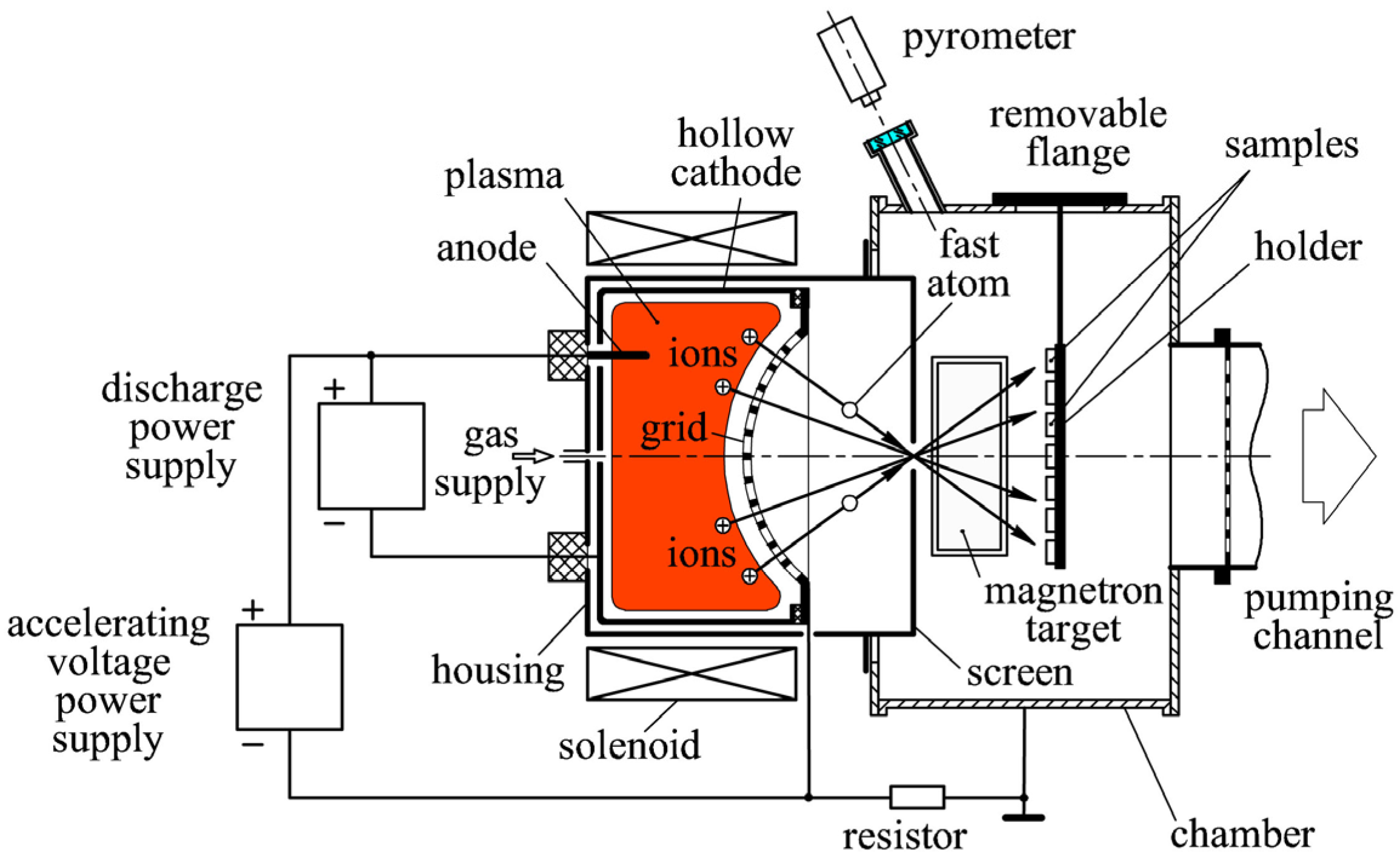
Figure 1. Experimental setup for stripping defective layers from dielectric ceramic samples.
Ceramics 07 00005 g001
Figure 2. Dependence of the step height δ on the target surface on distance x from the target center at solenoid current Is = 0 (line 1), 3 A (line 2) and 1.7 A (line 3).
Ceramics 07 00005 g002
Figure 3. Profilograms of the sample surfaces before etching with fast argon atoms.
Ceramics 07 00005 g003
Figure 4. SEM images of samples made of ZrO2 (a), Al2O3 (b) and Si3N4 (c) coated with TiB2 before (A) and after removal of defective surface layers (B).
Ceramics 07 00005 g004
Figure 5. Abrasion volume versus the test time for ceramic samples before treatment.
Ceramics 07 00005 g005
Figure 6. Dependence of the abrasion volume V on the test time t for ZrO2 sample before treatment (1), for ZrO2 sample with TiB2 coating (2) and for ZrO2 sample coated with TiB2 after removal of 6-µm-thick layer from its surface (3).
Ceramics 07 00005 g006
Figure 7. Dependence of the abrasion volume on the test time for Al2O3 sample before treatment (1), after deposition of TiB2 coating (2) and for Al2O3 sample coated with TiB2 after removal of 4.6-µm-thick layer from its surface (3).
Ceramics 07 00005 g007
Figure 8. Dependence of the abrasion volume on the test time for Si3N4 sample before treatment (1), after deposition of TiB2 coating (2) and for Si3N4 sample coated with TiB2 after removal of 3.2-µm-thick layer from its surface (3).
Ceramics 07 00005 g008
Table 1. Roughness of ceramic samples before and after etching by fast argon atoms.
The Sample MaterialZrO2Al2O3Si3N4
Roughness of the sample before etching, Ra (μm)0.1220.3040.105
Roughness of the sample after etching, Ra (µm)0.1140.2520.095
Disclaimer/Publisher’s Note: The statements, opinions and data contained in all publications are solely those of the individual author(s) and contributor(s) and not of MDPI and/or the editor(s). MDPI and/or the editor(s) disclaim responsibility for any injury to people or property resulting from any ideas, methods, instructions or products referred to in the content.