1. Introduction
Modern integrated circuits and electronic devices are mainly manufactured using single-crystal Si wafers produced using the Czochralski (CZ) pulling technique. The CZ method is based on crystal pulling from Si melt, for which a quartz crucible is placed in the hot zone to melt polysilicon. The quartz crucible is softened at high temperatures during the thermal pulling process; thus, the crucible must be secured by a graphite crucible to prevent deformation. Many types of defects are generated in Si ingots after thermal pulling, such as vacancies, interstitial defects, oxidation-induced stacking faults, and pits, because O from the quartz crucible diffuses into the Si ingot [
1,
2,
3,
4,
5,
6,
7].
Quartz is a mineral comprising Si and O atoms in a continuous SiO
4 tetrahedral framework, with each O atom shared between two tetrahedra, resulting in the overall chemical formula of SiO
2. Si inclusions and worm-like cristobalite SiO
2 appear locally at the Si–SiO
2 interface because of the solution–precipitation mechanism, as was demonstrated through scanning electron microscopy (SEM) [
8]. Local cristobalite SiO
2 can result in crack formation on the Si surface. When the Ba concentration in silica glass is >30 ppm, cristobalite SiO
2 changes to a dense, smooth, continuous layer and results in decreased precipitation of Si inclusions and defects [
9,
10]. The Ba-doped cristobalite layer is formed through heterogeneous nucleation caused by Ba additives. In addition to Ba additives [
9,
10], high-purity silica [
11], Si
3N
4 [
12,
13,
14], and SiC [
15] coatings on a crucible can considerably affect the lifetime of Si ingots. A high-purity silica and SiC coating on a crucible can act as a diffusion barrier layer and improve ingot quality [
11,
15]. Most crucibles used for single-crystal Si growth are made from SiO
2 (quartz), but alternative ceramic materials for use in Si crystal growth have gained research attention. Lin et al. [
16] studied three types of ceramic plates—Al
2O
3, ZrO
2, and quartz (SiO
2)—for contact with a Si wafer through annealing at 1450 °C, and they noted that defects appeared at the Si–ceramic interface. Using SEM and transmission electron microscopy (TEM), they found a crack and a dislocation pile-up at the Si–SiO
2 interface; two intermetallic compounds, Y
2Si
2O
7 and ZrSi
2, at the Si–ZrO
2 interface; and no intermetallic compounds and few defects at the Si–Al
2O
3 interface. Furthermore, the oxygen concentration and electrical resistivity near the interface were high, and they gradually decreased as the distance from the Si–ceramic interface increased [
16]. Therefore, the ceramics in contact with Si could result in defect formation, oxygen aggregation, and/or the reaction barrier layers on the surface of Si. It is significant to clarify which types of ceramics affect the defects, oxygen diffusion, and resistivity change at the Si interface after being in contact with Si. The purpose of the present study is to choose different valance electrons of ceramics, such as Mg
2+, Al
3+, La
3+, Y
3+, and Ti
4+, to place in contact with Si and then evaluate the electrical property of Si due to the charge balance effect and the formation of defects and effective barrier layers on the Si–ceramics. In the present study, 10 wt% ceramics—Al
2O
3, La
2O
3, Y
2O
3, MgO, and TiO
2—were separately added to amorphous SiO
2 after pressing and annealing at 1300 °C for single-crystal Si growth. The microstructures of the Si/SiO
2–additive interfaces were characterized using SEM and TEM in conjunction with energy-dispersive spectroscopy (EDS). In addition, the concentration of O and the resistivity of the Si after contact with the ceramics were measured and are discussed herein.
2. Experimental Procedures
Al
2O
3 (aluminum oxide power, Sigma-Aldrich, St. Louis, MO, USA, ≤10 μm, 99.5%), La
2O
3 (lanthanum oxide, Cerac, Inc., Milwaukee, WI, USA 325 mesh, 99.9%), Y
2O
3 (yttrium oxide, Sigma-Aldrich, St. Louis, MO, USA, 99.999%), MgO (magnesium oxide nano powder, Inframat Advanced Materials, Manchester, CT, USA, 30-nm, 99.9%), and TiO
2 (titanium oxide, NOAH Technologies, San Antonio, TX, USA, 325 mesh, 99.9%) powders (10 wt.%) were separately added to amorphous SiO
2 (quartz (silicon dioxide), UniRegion Bio-Tech, Hsinchu, Taiwan, 40 nm, 99.9%) powder and pressed at 5 tons for 1 min to obtain one-inch discs (thickness ≈ 2 mm). These green bodies were placed in an atmospheric furnace after sintering at 1300 °C for 2 h (
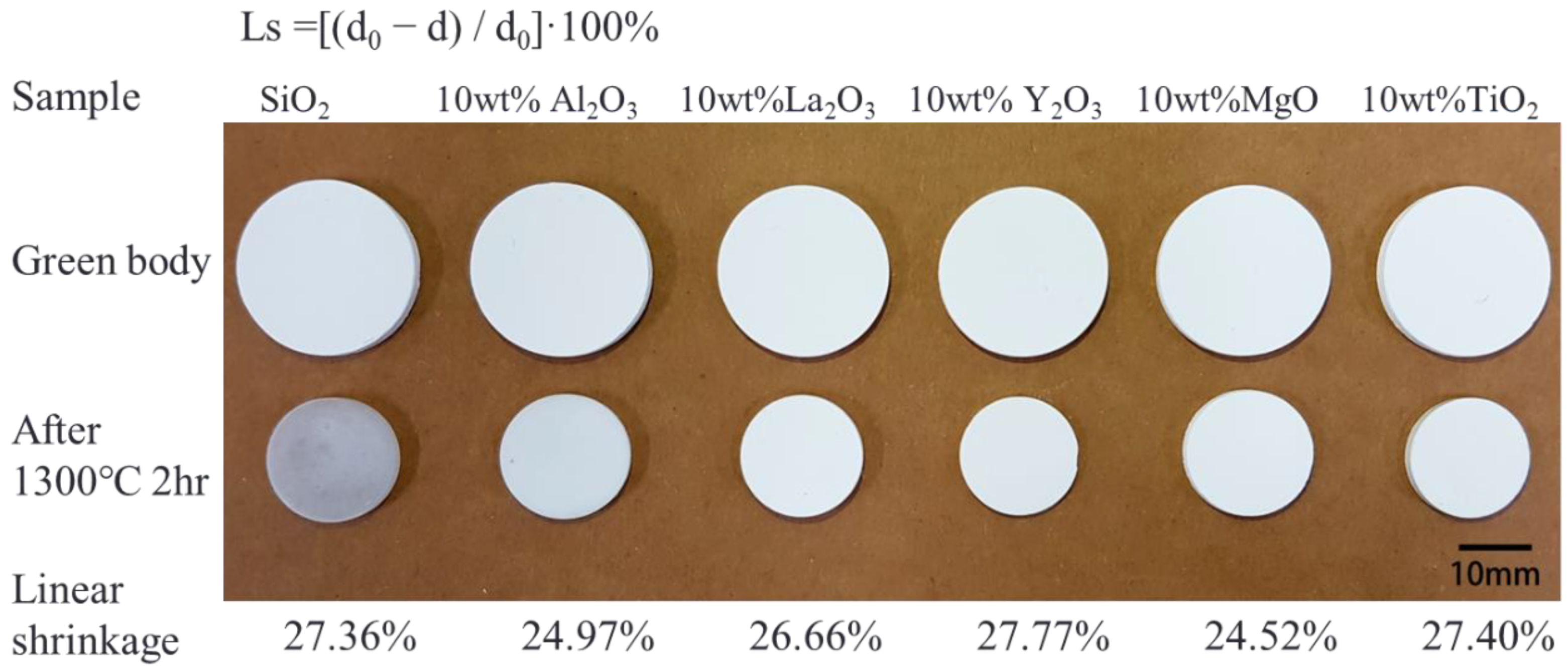
Figure 1).
Figure 1 shows a photograph of the green bodies and sintered SiO
2 and SiO
2 with ceramic additives, showing the volume shrinkage and color change in all the samples after sintering. Linear shrinkage was calculated using the formula
Ls = [(
d0 − d)/
d0) × 100%], where
Ls is the linear shrinkage,
d0 is the diameter of the green body, and
d is the diameter of the sintered sample. The linear shrinkage of all sintered samples was similar: 27.36% for SiO
2, 24.97% for SiO
2 with 10 wt.% Al
2O
3, 26.66% for SiO
2 with 10 wt.% La
2O
3, 27.77% for SiO
2 with 10 wt.% Y
2O
3, 24.52% for SiO
2 with 10 wt.% MgO, and 27.40% for SiO
2 with 10 wt.% TiO
2. The densities of all sintered samples were calculated using the Archimedes method, and the relative densities were ~90%. Next, the sintered samples were interfaced with Si (p-type-doped boron, CZ growth method, orientation of [100], resistivity ≈ 15–25 Ω·cm, thickness = 655–695 μm, O content = 12.00–15.00 ppm) to evaluate the reaction between the Si and the SiO
2 with ceramic additives. Then, the sintered SiO
2–ceramics were ground, polished, and interfaced with Si in a rectangular graphite crucible with inner dimensions of 23 × 23 × 20 mm
3 and outer dimensions of 33 × 33 × 25 mm
3, as shown in
Figure 2a,b. The crucibles containing the Si/SiO
2–ceramics were placed in a vacuum furnace, vacuumed to approximately 10
−4 Torr, and annealed at 1450 °C (slightly higher than the melting temperature of Si: 1414 °C) under an Ar atmosphere. After holding this temperature for 30 min, the furnace was cooled to room temperature; then, the graphite crucibles were cut and removed, as shown in
Figure 2c. For the O concentration and Si resistivity measurements after the reactions between the Si and SiO
2–ceramics, several pieces of Si were cut longitudinally with respect to the interface, as shown in
Figure 2c. For the phase identification and microstructural characterization of the SiO
2–ceramics, SEM (Model JSM 6500F, JEOL Ltd., Tokyo, Japan), TEM (Model JEM 2010F, JEOL Ltd., Tokyo, Japan), and X-ray diffraction (XRD; X’Pert Pro MRD, Malvern Panalytical Ltd., Malvern, UK) were performed before contact with Si. The crystal structure of the reaction products at the interface was characterized by selected area diffraction patterns (SADPs) of TEM and EDS. The Inorganic Crystal Structure Database (ICSD), Joint Committee on Powder diffraction Standards (JCPDS) database and crystallographic software (Diamond version 3.0 and CaRIne Crystallography 3.1) were used for the identification of the crystal structures of the phases. The cross-sectional TEM specimens of Si–ceramic joints were prepared by conventional mechanical polishing and focused ion beam (FIB, FEI NovaLab 600). The quantitative composition analyses were performed based on the principle of the Cliff–Lorimer [
17] standard-less method. Additionally, in order to accurately calculate the lattice parameters of reaction products, the image magnification of TEM was calibrated using the MAG*I*CAL reference standard sample (Norrox Scientific Ltd., Beaver Pond, ON, Canada). The pieces of Si from Si–ceramic joints were cut along a direction longitudinal to the interface for the residual oxygen and resistivity measurements. The concentration evaluation of the residual oxygen in Si by Fourier-transform infrared spectroscopy (FTIR, Bruker VERTEX 70) was performed based on the ASTM F 1188 method [
18], and the resistivity of Si was measured by four-point probe resistance meter (RT-80, Napson Corporation, Tokyo, Japan).
3. Results and Discussion
Figure 3 shows the XRD spectra of the pure SiO
2 and the SiO
2 with 10 wt.% Al
2O
3, La
2O
3, Y
2O
3, MgO, and TiO
2. Before sintering, the crystal structure of the SiO
2 tended to be in the amorphous phase (broad peak at ~20°) and then changed to a combination of the amorphous phase and cristobalite tetragonal phase (reference code: 01-076-0940, crystal system: tetragonal, space group: P41212(92),
a =
b = 4.9964 Å,
c = 7.0169 Å,
α =
β =
γ = 90°) after sintering at 1300 °C, as indicated by the sharp peak at ~20° in
Figure 3a. The Al
2O
3 and TiO
2 additives did not react with the SiO
2 to form other phases (
Figure 3b,f). The other ceramic additives, La
2O
3, Y
2O
3, and MgO, reacted with the SiO
2 to form other reaction phases in the samples. For example, La
2Si
2O
7, Y
2Si
2O
7, and MgSiO
3 (Mg
2SiO
4) phases were found with the addition of 10 wt.% La
2O
3 (
Figure 3c), Y
2O
3 (
Figure 3d), and MgO (
Figure 3e), respectively. The corresponding chemical formulas are 2SiO
2 + La
2O
3 = La
2Si
2O
7, 2SiO
2 + Y
2O
3 = Y
2Si
2O
7, and SiO
2 + MgO = MgSiO
3 or SiO
2 + 2MgO = Mg
2SiO
4.
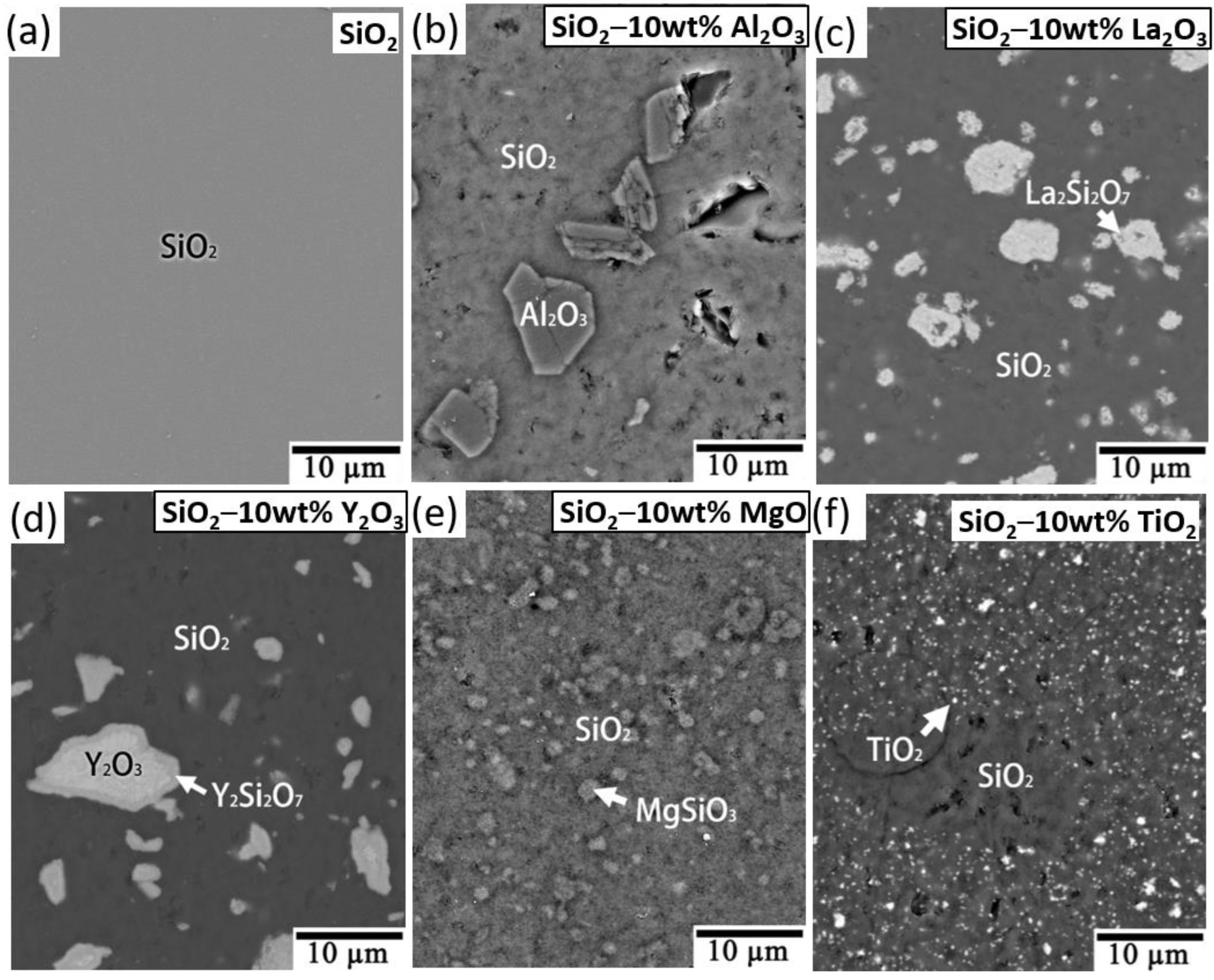
Figure 4 shows the SEM and backscattered electron images (BEIs) for the SiO
2 and the SiO
2 with 10 wt.% Al
2O
3, La
2O
3, Y
2O
3, MgO, and TiO
2 additives, showing that no other reaction phase was formed after the addition of Al
2O
3 (
Figure 4b) or TiO
2 (
Figure 4f). However, the reaction phases La
2Si
2O
7, Y
2Si
2O
7, and MgSiO
3 were found with the La
2O
3 (
Figure 4c), Y
2O
3 (
Figure 4d), and MgO (
Figure 4e) additives. The reaction phases were further confirmed using TEM.
Figure 5 shows the TEM bright-field images (BFIs) and the selected area diffraction patterns (SADPs) of the Si with 10 wt.% Al
2O
3, La
2O
3, Y
2O
3, MgO, and TiO
2 additives after sintering at 1300 °C in Ar. Through SADP indexing and EDS and TEM, the composition of Al
2O
3, La
2Si
2O
7, Y
2Si
2O
7, MgSiO
3, and TiO
2 (
Figure 6f) and the reaction phases (La
2Si
2O
7, Y
2Si
2O
7, and MgSiO
3) in the SiO
2 with ceramic additives were identified.
Through XRD (
Figure 3), SEM (
Figure 4), and TEM (
Figure 5), the microstructures and reaction phases were thoroughly examined in the sintered SiO
2–ceramic additives. After the reaction between the Si and the sintered SiO
2–ceramic additives, two types of microstructures were identified: those with and those without a reaction layer at the interface.
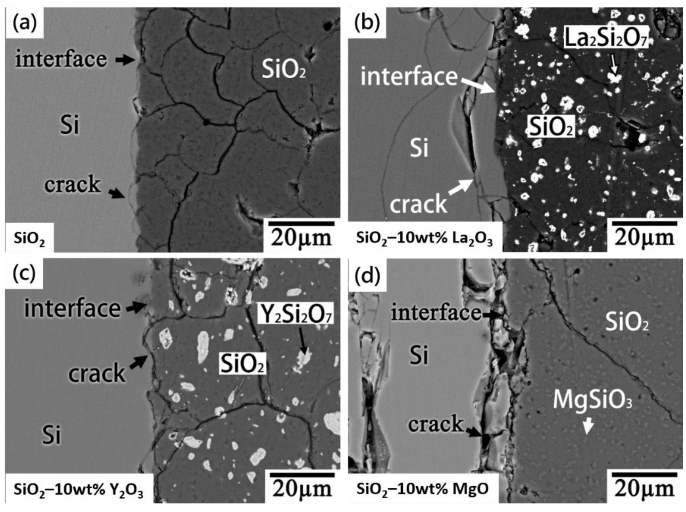
Figure 6 shows the BEIs/SEM images for the Si/SiO
2 and Si/SiO
2–La
2O
3, Si/SiO
2–Y
2O
3, and Si/SiO
2–MgO interfaces, showing the absence of a reaction layer. Cracks formed in the Si and SiO
2–ceramics because of a coefficient of thermal expansion (CTE) mismatch. XRD (
Figure 3) revealed amorphous SiO
2 (broad peak) and cristobalite SiO
2 in the SiO
2 and SiO
2–ceramics. The difference in the CTEs of amorphous SiO
2 (0.5 × 10
−6/K) [
19] and cristobalite SiO
2 (14.5 × 10
−6/K) [
20] is large and, thus, resulted in cracks in the SiO
2 (
Figure 6a). In
Figure 6b–d, cracks are observable in the SiO
2–ceramics (with 10 wt.% La
2O
3, Y
2O
3, and MgO) because of the CTE mismatch between the SiO
2 and the reaction phases La
2Si
2O
7 (6 × 10
−6/K) [
21], Y
2Si
2O
7 (3.9 × 10
−6/K) [
22], and MgSiO
3 (47.7 × 10
−6/K) [
23]. The CTEs of cristobalite SiO
2, La
2Si
2O
7, Y
2Si
2O
7, and MgSiO
3 are larger than those of Si (2.6 × 10
−6/K) [
24]. Therefore, the Si endured compressive stress at the SiO
2 site, resulting in cracks near the interface. Furthermore, the CTE of MgSiO
3 is high (~47.7 × 10
−6/K) and, therefore, resulted in severe cracks in the Si near the interface (
Figure 6d).
O in Si severely hinders Si ingot growth [
3,
4]. To evaluate the O content in the Si near and far from the Si–SiO
2 interface, EDS line scanning of TEM was performed.
Figure 7 shows the BFIs/TEM images and EDS line scans of the Si/–SiO
2, Si/SiO
2–La
2O
3, Si/SiO
2–Y
2O
3, and Si/SiO
2–MgO interfaces, showing the elemental distribution at the SiO
2 and Si sites. The O content was approximately 10 at.% in the Si near the interface for the SiO
2 with no ceramic additives (
Figure 7a). When ceramics were added, the O content in the Si near the interface decreased to approximately 3 at.% for the La
2O
3 additive (
Figure 7b) and approximately 8 at.% for the Y
2O
3 and MgO additives (
Figure 7c,d).
A reaction layer formed at the interface of the Si with SiO
2–Al
2O
3 and SiO
2–TiO
2, as shown in the BEIs/SEM images in
Figure 8. TEM was used to analyze the reaction layer at the interface (
Figure 9).
Figure 9a,b show the BFIs/TEM images, EDS line scans, and SADPs for the Si/SiO
2–Al
2O
3 and Si/SiO
2–TiO
2 interfaces, respectively. No diffraction spots were found in the SADP of the reaction layer or the cristobalite SiO
2, as shown by the spot patterns (white arrows) in the SADP shown in
Figure 9a,b. The reaction layer mainly comprised Si and O, as well as small quantities of Al (~8 at.%) and Ti (~2 at.%), as shown in the EDS images in
Figure 9a,b, respectively. From the SADP and EDS results, the reaction layer could be identified as amorphous SiO
2 with small quantities of dissolved Al or Ti. Furthermore, the amorphous SiO
2 reaction layer effectively restricted O diffusion into the Si, as indicated by the O content of approximately 2 at.% and <0.8 at.% in the EDS line scans in
Figure 9a,b, respectively. The mechanism underlying the formation of the amorphous SiO
2 reaction layer is shown in
Figure 10.
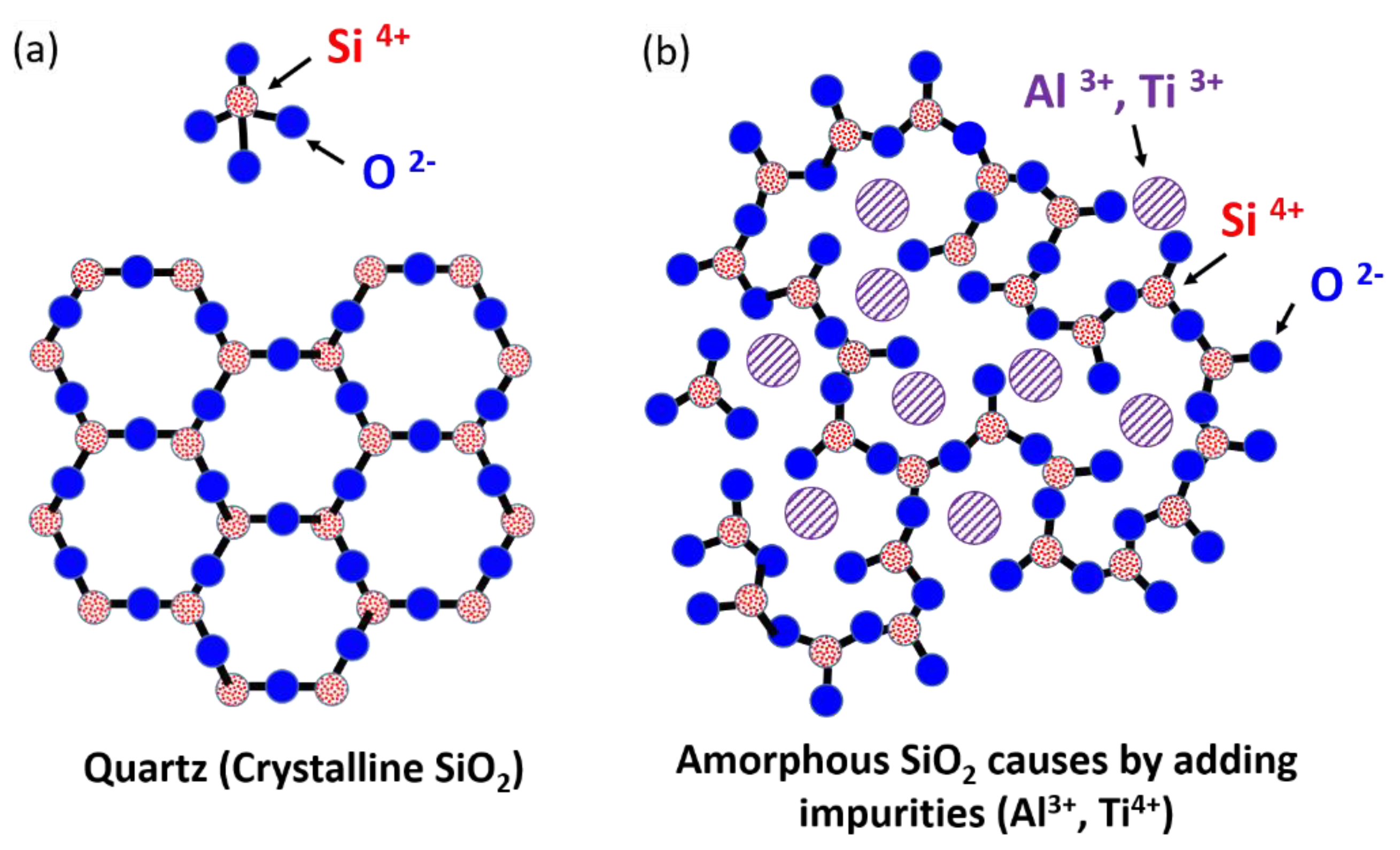
Figure 10a shows a schematic of crystalline SiO
2, revealing the tetrahedral arrangement of one Si atom bonded to four O atoms; in the image, most O atoms are bridged to two Si atoms, and two tetrahedra are joined at a corner to form the regular crystal structure of quartz. When the SiO
2–Al
2O
3 and SiO
2–TiO
2 came into contact with the Si substrate, the Si, O, Al, and Ti atoms diffused toward the Si site. The O from the SiO
2 site easily diffused into the Si substrate; this finding is supported by the diffusivity of the Al (1.073 × 10
−11 cm
2/s) [
25], Ti (1.162 × 10
−8 cm
2/s) [
26], Si (8.610 × 10
−14 cm
2/s) [
27], and O (1.429 × 10
−10 cm
2/s) [
28] in the Si at 1200 °C. The results indicate that Al atoms could remain at the SiO
2 site because of their lower diffusivity than that of the O near the interface. Another possible explanation is the formation of native oxynitride on the Si surface, which blocks Al and Ti diffusion into the Si [
29]. Thus, numerous Al and Ti atoms aggregated at the SiO
2 near the interface and resulted in the formation of amorphous SiO
2 because of the replacement of the Si position in the SiO
2 with Al
3+ and Ti
4+ impurities, which can break the bonds between Si and O, as shown in
Figure 10b [
30].
For the O content and resistivity measurements, several (~800 µm thick) pieces of Si were cut longitudinally with respect to the interface after contact between the Si and SiO
2 with additives, as shown in
Figure 2d.
Figure 11a shows the distribution of the O concentration in the Si pieces and the distance from the Si/SiO
2–ceramic interface, as measured through FTIR spectroscopy. The O concentration of the Si was 10.5–13.2 × 10
17 atoms/cm
3 (12–15 ppm) before contact with the SiO
2. The O concentration of the Si after contact with SiO
2 decreased to ~6–9 × 10
17 atoms/cm
3, probably because of SiO evaporation during the heat treatment. However, the O concentrations of all the SiO
2–ceramics were lower than those of the pure SiO
2. Among them, the O concentrations of SiO
2–Al
2O
3 and SiO
2–MgO were less than 10
16, implying that ceramic additives in SiO
2 affect the diffusion of O into the Si substrate.
Figure 11b shows the electrical resistivity of the Si pieces at various distances from the interface of the Si/SiO
2–ceramics, as measured using a four-point probe resistance meter. Similarly, the electrical resistivity of the Si near the interface was high and gradually decreased away from the interface for all samples. For example, the resistivity of the Si near the interface was approximately 5 Ω·cm and decreased to as low as 3 Ω·cm far from the Si/SiO
2 interface. The resistivity of the Si was 21.85 Ω·cm before contact with the SiO
2. As anticipated, the resistivity of the Si both near and far from the Si–ceramic interface was lower than that of pure Si. Hull [
31] indicated that unintentional O diffusion into Si usually manifests as n-type doping (with SiO
4 as the donor) and results in a decrease in the resistivity of Si. When Si comes into contact with SiO
2, the O from the SiO
2 diffuses into the Si, causing a decrease in resistivity; this is supported by our resistivity measurements shown in
Figure 11b. The resistivity of the Si with all additives (0.12, 0.24, 0.21, 0.36, and 0.30 Ω·cm for Y
2O
3, La
2O
3, TiO
2, Al
2O
3, and MgO, respectively) was less than that of the Si (~3 Ω·cm) in contact with the pure SiO
2. When Al
3+, La
3+, and Y
3+ ions diffused and replaced one or two (for Mg
2+) Si atoms in the substrate, the remaining valence electrons were insufficient to satisfy the four covalent neighboring bonds of the Si, resulting in the formation of holes. Thus, the Al, La, and Y(IIIA) atoms became acceptors. As for the diffusion of the Ti and the Si originating from the SiO
2 into the Si substrate, the electrical property of the Si substrate could not be changed because of the charge balance effect (Si
4+ = Ti
4+). However, the dissolution of Al, Mg, Y, La, Ti, Y, and O impurities in the Si substrate resulted in interstitial or vacancy defects, thus affecting the resistivity.


