
Enabling Sustainable Solar Energy Systems Through Electromagnetic Monitoring of Key Components Across Production, Usage, and Recycling: A Review

Abstract
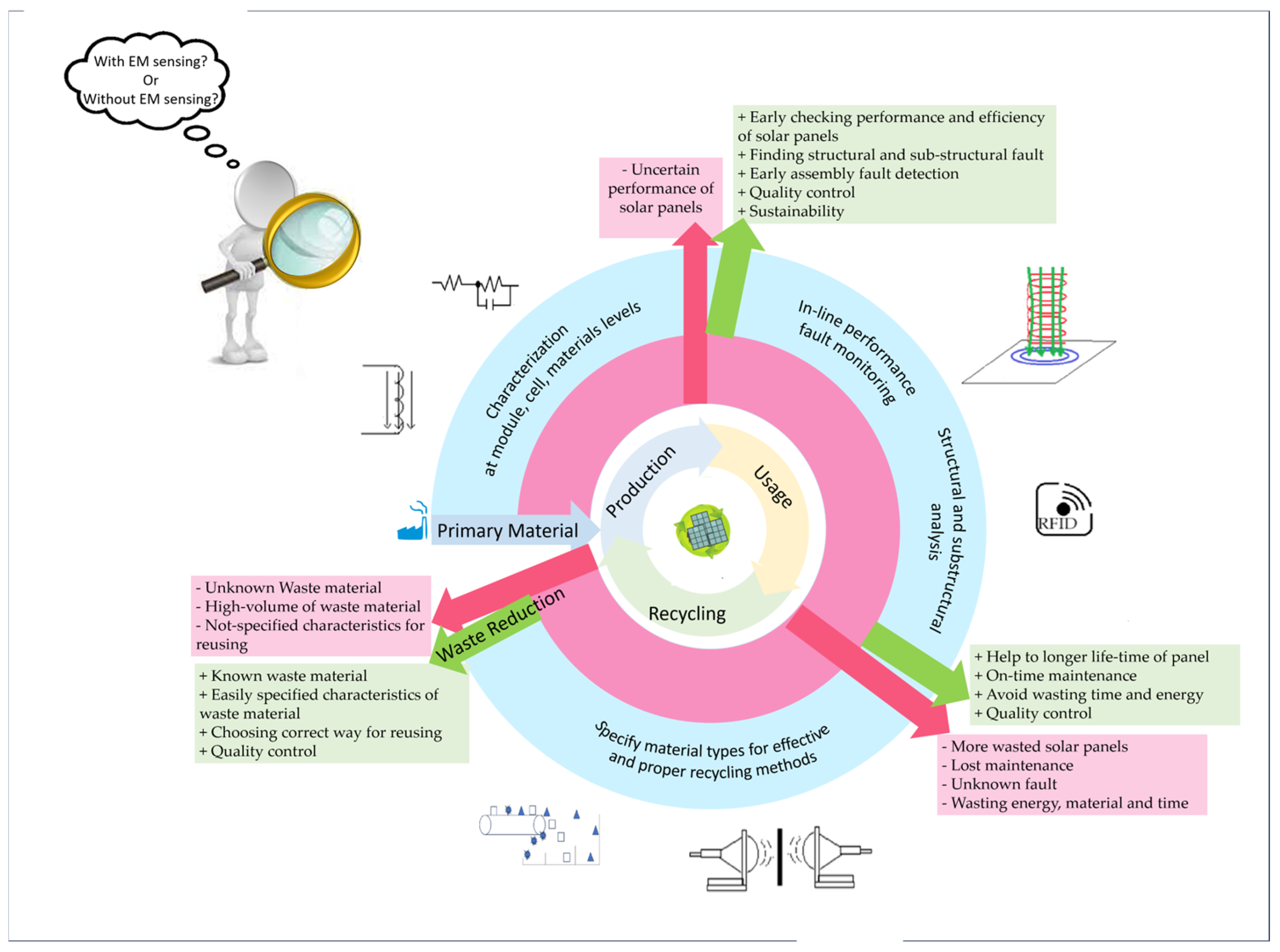
1. Introduction
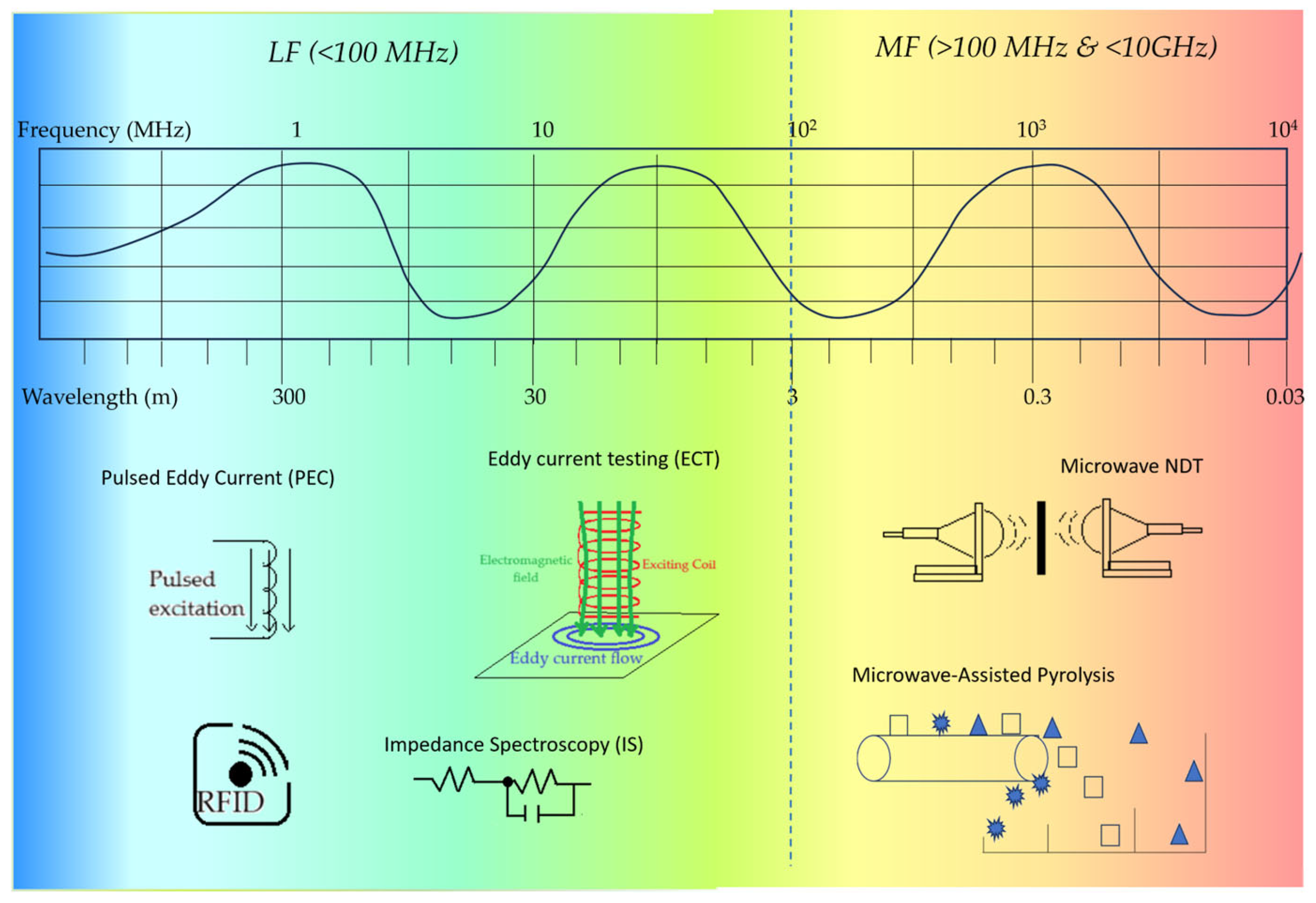
2. Electromagnetic Monitoring Methods in Production–Usage–Recycling Cycle of Key Components of Solar Energy
2.1. Low-Frequency Electromagnetic (LF-EM) Methods (<100 MHz)
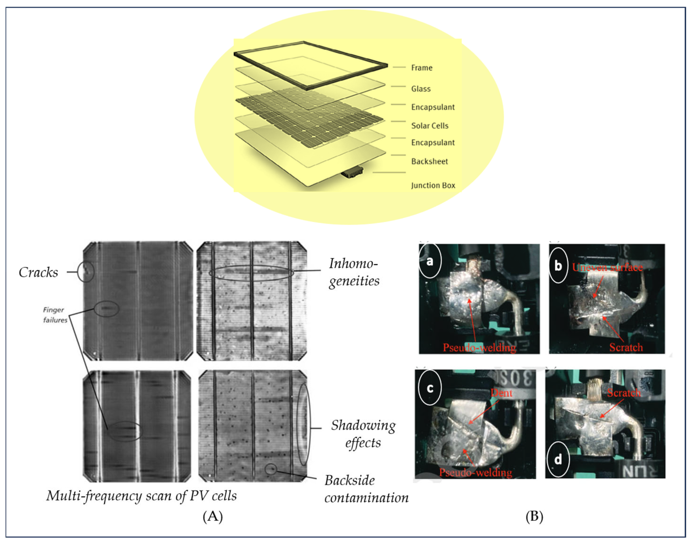
2.1.1. In Production
2.1.2. In Usage
2.1.3. In Recycling
- Elimination of consumables and chemical inputs;
- Continuous processing capability without the need for pretreatment;
- Reduced maintenance requirements due to non-contact operation.
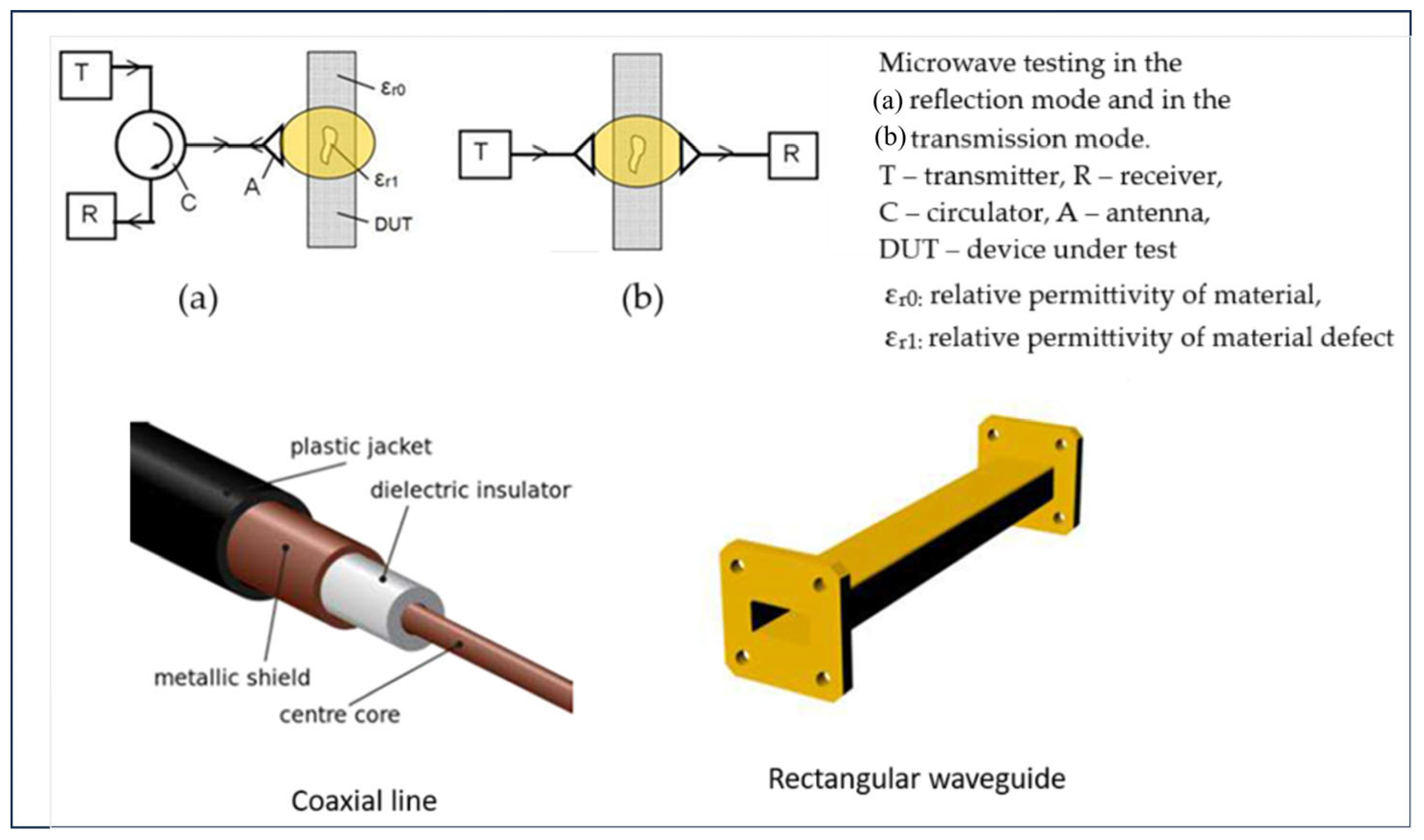
2.2. Medium-Frequency Electromagnetic (MF-EM) Methods (100 MHz–10 GHz)
2.2.1. In Production
2.2.2. In Usage
2.2.3. In Recycling
3. Challenges, Future Trends, and Opportunities
3.1. Advantages of EM Techniques for Sustainable Manufacturing
3.2. Challenges and Limitations
3.3. Future Trends and Opportunities
4. Conclusions
Funding
Conflicts of Interest
Abbreviations
| AI | artificial intelligence |
| BP | backpropagation |
| CNNs | convolutional neural networks |
| CSP | concentrating solar thermal power |
| DS | dielectric spectroscopy |
| ECS | electrodynamic eddy current separation |
| ECT | eddy current testing |
| ECI | eddy current imaging |
| EM | electromagnetic |
| EVA | ethylene–vinyl acetate |
| GNNs | graph neural networks |
| IS | impedance spectroscopy |
| IEA | International Energy Agency |
| IEA-PVPS | IEA Photovoltaic Power Systems Programme |
| LF-EM | low-frequency electromagnetic |
| MF-EM | medium-frequency electromagnetic |
| ML | machine learning |
| MPS | Microwave Photonic Sensing |
| MPT | Microwave Phased Testing |
| MR | microwave reflectometry |
| NDT | Non-Destructive Testing |
| OSCs | organic solar cells |
| PEC | pulsed eddy current testing |
| PID | Potential Induced Degradation |
| PMR | Passive Microwave Radiometry |
| PSCs | perovskite solar cells |
| PUR | Production–Usage–Recycling |
| PV | photovoltaic |
| RFID | Radio Frequency Identification |
| SMEs | Small and Medium-sized Enterprises |
| TCO | Transparent Conductive Oxide |
| UAV | unmanned aerial vehicle |
References
- O’Brien, C. Global Manufacturing and the Sustainable Economy. Int. J. Prod. Res. 2002, 40, 3867–3877. [Google Scholar] [CrossRef]
- Nooman AlMallahi, M.; Al Swailmeen, Y.; Ali Abdelkareem, M.; Ghani Olabi, A.; Elgendi, M. A Path to Sustainable Development Goals: A Case Study on the Thirteen Largest Photovoltaic Power Plants. Energy Convers. Manag. X 2024, 22, 100553. [Google Scholar] [CrossRef]
- Hasan, M.M.; Hossain, S.; Mofijur, M.; Kabir, Z.; Badruddin, I.A.; Yunus Khan, T.M.; Jassim, E. Harnessing Solar Power: A Review of Photovoltaic Innovations, Solar Thermal Systems, and the Dawn of Energy Storage Solutions. Energies 2023, 16, 6456. [Google Scholar] [CrossRef]
- Chatzipanagi, A.; Jaeger-Waldau, A.; Letout, S.; Mountraki, A.; Gea, B.J.; Georgakaki, A.; Ince, E.; Schmitz, A. Clean Energy Technology Observatory: Photovoltaics in the European Union-2024 Status Report on Technology Development, Trends, Value Chains and Markets; Publications Office of the European Union: Luxembourg, 2022. [Google Scholar]
- Hepburn, C.; Qi, Y.; Stern, N.; Ward, B.; Xie, C.; Zenghelis, D. Towards Carbon Neutrality and China’s 14th Five-Year Plan: Clean Energy Transition, Sustainable Urban Development, and Investment Priorities. Environ. Sci. Ecotechnology 2021, 8, 100130. [Google Scholar] [CrossRef]
- Net Zero by 2050 Data Explorer—Data Tools. Available online: https://www.iea.org/data-and-statistics/data-tools/net-zero-by-2050-data-explorer (accessed on 10 June 2025).
- Guo, J.; Cheng, Y.; Song, X. Sustainable Photovoltaic Recycling to Mitigate Environmental Pollution under Climate and Resource Constraints. J. Ind. Ecol. 2025, 29, 330–343. [Google Scholar] [CrossRef]
- Aleksandra, A.; Sara, B.P.; Małgorzata, J.; Brian, B.; Davide, P.; Miguel, C. Role of Solar PV in Net-Zero Growth: An Analysis of International Manufacturers and Policies. Prog. Photovolt. Res. Appl. 2024, 32, 607–622. [Google Scholar] [CrossRef]
- Iturralde Carrera, L.A.; Garcia-Barajas, M.G.; Constantino-Robles, C.D.; Álvarez-Alvarado, J.M.; Castillo-Alvarez, Y.; Rodríguez-Reséndiz, J. Efficiency and Sustainability in Solar Photovoltaic Systems: A Review of Key Factors and Innovative Technologies. Eng 2025, 6, 50. [Google Scholar] [CrossRef]
- International Energy Agency Photovoltaic Power Systems Programme. PVPS Task 13: Performance and Failure Analysis of Photovoltaic Systems—Annex: Degradation and Failure; IEA-PVPS: Redfern, NSW, Australia, 2025. [Google Scholar]
- Chun, Y.; Bidanda, B. Sustainable Manufacturing and the Role of the International Journal of Production Research. Int. J. Prod. Res. 2013, 51, 7448–7455. [Google Scholar] [CrossRef]
- Dhanraj, J.A.; Mostafaeipour, A.; Velmurugan, K.; Techato, K.; Chaurasiya, P.K.; Solomon, J.M.; Gopalan, A.; Phoungthong, K. An Effective Evaluation on Fault Detection in Solar Panels. Energies 2021, 14, 7770. [Google Scholar] [CrossRef]
- Hwang, B.; Hillmann, S.; Schulze, M.; Klein, M.; Heuer, H. Eddy Current Imaging for Electrical Characterization of Silicon Solar Cells and TCO Layers. In Proceedings of the Smart Materials and Nondestructive Evaluation for Energy Systems 2015, San Diego, CA, USA, 9–10 March 2015; SPIE: Bellingham, WA, USA, 2015; Volume 9439, pp. 70–78. [Google Scholar]
- Matacena, I.; Lancellotti, L.; Lisi, N.; Delli Veneri, P.; Guerriero, P.; Daliento, S. Impedance Spectroscopy for the Characterization of the All-Carbon Graphene-Based Solar Cell. Energies 2020, 13, 1908. [Google Scholar] [CrossRef]
- Matacena, I.; Guerriero, P.; Lancellotti, L.; Alfano, B.; De Maria, A.; La Ferrara, V.; Mercaldo, L.V.; Miglietta, M.L.; Polichetti, T.; Rametta, G.; et al. Impedance Spectroscopy Analysis of Perovskite Solar Cell Stability. Energies 2023, 16, 4951. [Google Scholar] [CrossRef]
- Al Mahdi, H.; Leahy, P.G.; Alghoul, M.; Morrison, A.P. A Review of Photovoltaic Module Failure and Degradation Mechanisms: Causes and Detection Techniques. Solar 2024, 4, 43–82. [Google Scholar] [CrossRef]
- IEC 61215-1: 2021; Terrestrial Photovoltaic (PV) Modules—Design Qualification and Type Approval—Part 1: Test Requirements. International Electrotechnical Commission: Geneva, Switzerland, 2021.
- Köntges, M.; Kajari-Schröder, S.; Kunze, I.; Jahn, U. Crack Statistic of Crystalline Silicon Photovoltaic Modules. In Proceedings of the 26th European Photovoltaic Solar Energy Conference and Exhibition, Hamburg, Germany, 5–9 September 2011; Volume 26, pp. 3290–3294. [Google Scholar]
- Zoughi, R.; Ganchev, S. Microwave Nondestructive Evaluation; Colorado State University: Fort Collins, CO, USA, 1995. [Google Scholar]
- Kharkovsky, S.; Zoughi, R. Microwave and Millimeter Wave Nondestructive Testing and Evaluation-Overview and Recent Advances. IEEE Instrum. Meas. Mag. 2007, 10, 26–38. [Google Scholar] [CrossRef]
- Sophian, A.; Tian, G.Y.; Taylor, D.; Rudlin, J. Electromagnetic and Eddy Current NDT: A Review. Insight 2001, 43, 302–306. [Google Scholar]
- Ahamer, G. Potentials and Costs for the Transition of Decentralised Energy Infrastructure in Europe. Int. J. Glob. Environ. Issues 2023, 22, 171–197. [Google Scholar] [CrossRef]
- Breit, T.P. Balcony PV Power Plants in Austria: Public Support for Adoption and Differences in Implementation Between Austria and Germany. PhD Thesis, Technische Universität Wien, Vienna, Austria, 2023. [Google Scholar]
- Deng, Y.; Liu, X. Electromagnetic Imaging Methods for Nondestructive Evaluation Applications. Sensors 2011, 11, 11774–11808. [Google Scholar] [CrossRef]
- Dallas, W.; Polupan, O.; Ostapenko, S. Resonance Ultrasonic Vibrations for Crack Detection in Photovoltaic Silicon Wafers. Meas. Sci. Technol. 2007, 18, 852. [Google Scholar] [CrossRef]
- Deriche, M.; Raad, M.W.; Suliman, W. An IOT Based Sensing System for Remote Monitoring of PV Panels. In Proceedings of the 2019 16th International Multi-Conference on Systems, Signals & Devices (SSD), Istanbul, Turkey, 21–24 March 2019; IEEE: Piscataway, NJ, USA, 2019; pp. 393–397. [Google Scholar]
- Doni, A.; Dughiero, F. Electrothermal Heating Process Applied to C-Si PV Recycling. In Proceedings of the 2012 38th IEEE Photovoltaic Specialists Conference, Austin, TX, USA, 3–8 June 2012; IEEE: Piscataway, NJ, USA; pp. 000757–000762. [Google Scholar]
- Akram, M.W.; Li, G.; Jin, Y.; Chen, X.; Zhu, C.; Shauket, I.; Ahmad, A. Defect Detection and Degradation Analysis in Photovoltaic Modules Using Thermography, Spectroscopy, and Current–Voltage Measurements, and Quantitative Assessment of Their Impact. Energy Technol. 2020, 8, 2000100. [Google Scholar] [CrossRef]
- Jackson, J.D. Classical Electrodynamics; John Wiley & Sons: Hoboken, NJ, USA, 1998. [Google Scholar]
- García-Martín, J.; Gómez-Gil, J.; Vázquez-Sánchez, E. Non-Destructive Techniques Based on Eddy Current Testing. Sensors 2011, 11, 2525–2565. [Google Scholar] [CrossRef]
- Zhong, X.; Sun, Q.; Chen, D.; Yuan, J.; Wang, F.; Chen, S.; Zhong, L. Effect of Eddy Current for Photovoltaic Module on Lightning-Induced Overvoltage Caused by Electromagnetic Coupling. IEEE Trans. Electromagn. Compat. 2023, 65, 850–861. [Google Scholar] [CrossRef]
- Papargyri, L.; Theristis, M.; Kubicek, B.; Krametz, T.; Mayr, C.; Papanastasiou, P.; Georghiou, G.E. Modelling and Experimental Investigations of Microcracks in Crystalline Silicon Photovoltaics: A Review. Renew. Energy 2020, 145, 2387–2408. [Google Scholar] [CrossRef]
- Wang, N.; Liu, X.; Zhou, B.; He, C.; Yang, J.; Wu, B. Eddy Current O-Scan and C-Scan Imaging Techniques for Macrocrack Detection in Silicon Solar Cells. Nondestruct. Test. Eval. 2019, 34, 389–400. [Google Scholar] [CrossRef]
- Tan, J.; Jia, S.; Ramakrishna, S. End-of-Life Photovoltaic Modules. Energies 2022, 15, 5113. [Google Scholar] [CrossRef]
- Sunny, A.I.; Tian, G.Y.; Zhang, J.; Pal, M. Low Frequency (LF) RFID Sensors and Selective Transient Feature Extraction for Corrosion Characterisation. Sens. Actuators A Phys. 2016, 241, 34–43. [Google Scholar] [CrossRef]
- Felsch, T.; Strauss, G.; Perez, C.; Rego, J.M.; Maurtua, I.; Susperregi, L.; Rodríguez, J.R. Robotized Inspection of Vertical Structures of a Solar Power Plant Using NDT Techniques. Robotics 2015, 4, 103–119. [Google Scholar] [CrossRef]
- Sophian, A.; Tian, G.; Fan, M. Pulsed Eddy Current Non-Destructive Testing and Evaluation: A Review. Chin. J. Mech. Eng. 2017, 30, 500–514. [Google Scholar] [CrossRef]
- Ennemri, A.; Logerais, P.O.; Balistrou, M.; Durastanti, J.F.; Belaidi, I. Cracks in Silicon Photovoltaic Modules: A Review. J. Optoelectron. Adv. Mater. 2019, 21, 74–92. [Google Scholar]
- Romero, B.; del Pozo, G.; Arredondo, B.; Martín-Martín, D.; Hernández-Balaguera, E.; González, M.d.C.L. Characterization of Organic and Perovskite Solar Cells by Impedance Spectroscopy. In Proceedings of the Women in Renewable Energy (WiRE), San Diego, CA, USA, 30 August 2019; SPIE: Bellingham, WA, USA, 2019; Volume 11095, p. 110950N. [Google Scholar]
- Aimaganbetov, K.; Yerezhep, D.; Kishkenebayev, M.; Chuchvaga, N.; Almas, N.; Tokmoldin, S.; Tokmoldin, N. Characterization of a Heterojunction Silicon Solar Cell by Means of Impedance Spectroscopy. Micromachines 2024, 15, 184. [Google Scholar] [CrossRef]
- von Hauff, E.; Klotz, D. Impedance Spectroscopy for Perovskite Solar Cells: Characterisation, Analysis, and Diagnosis. J. Mater. Chem. C 2022, 10, 742–761. [Google Scholar] [CrossRef]
- Erdil, U.; Khenkin, M.; Bernardes De Araujo, W.M.; Emery, Q.; Lauermann, I.; Paraskeva, V.; Norton, M.; Vediappan, S.; Kumar, D.K.; Gupta, R.K.; et al. Delamination of Perovskite Solar Cells in Thermal Cycling and Outdoor Tests. Energy Tech. 2025, 13, 2401280. [Google Scholar] [CrossRef]
- Sinha, A.; Bliss, M.; Wu, X.; Roy, S.; Gottschalg, R.; Gupta, R. Cross-Characterization for Imaging Parasitic Resistive Losses in Thin-Film Photovoltaic Modules. J. Imaging 2016, 2, 23. [Google Scholar] [CrossRef]
- Węglarski, M.; Jankowski-Mihułowicz, P.; Chamera, M.; Dziedzic, J.; Kwaśnicki, P. Designing Antennas for RFID Sensors in Monitoring Parameters of Photovoltaic Panels. Micromachines 2020, 11, 420. [Google Scholar] [CrossRef] [PubMed]
- Węglarski, M.; Jankowski-Mihułowicz, P.; Kamuda, K.; Pyt, P.; Pitera, G.; Lichoń, W.; Chamera, M.; Ciejka, C. RFID Sensors for Monitoring Glazing Units Integrating Photovoltaic Modules. Energies 2022, 15, 1401. [Google Scholar] [CrossRef]
- Solar, H.; Beriain, A.; Rezola, A.; Del Rio, D.; Berenguer, R. A 22-m Operation Range Semi-Passive UHF RFID Sensor Tag with Flexible Thermoelectric Energy Harvester. IEEE Sens. J. 2022, 22, 19797–19808. [Google Scholar] [CrossRef]
- Solar, H.; Beriain, A.; Berenguer, R.; Sosa, J.; Montiel-Nelson, J.A. Semi-Passive UHF RFID Sensor Tags: A Comprehensive Review. IEEE Access 2023, 11, 135583–135599. [Google Scholar] [CrossRef]
- Smith, Y.R.; Nagel, J.R.; Rajamani, R.K. Electrodynamic Eddy Current Separation of End-of-Life PV Materials. In Energy Technology 2017; Zhang, L., Drelich, J.W., Neelameggham, N.R., Guillen, D.P., Haque, N., Zhu, J., Sun, Z., Wang, T., Howarter, J.A., Tesfaye, F., et al., Eds.; Springer International Publishing: Cham, Switzerland, 2017; pp. 379–386. [Google Scholar]
- Smith, Y.R.; Nagel, J.R.; Rajamani, R.K. Eddy Current Separation for Recovery of Non-Ferrous Metallic Particles: A Comprehensive Review. Miner. Eng. 2019, 133, 149–159. [Google Scholar] [CrossRef]
- Preet, S.; Smith, S.T. A Comprehensive Review on the Recycling Technology of Silicon Based Photovoltaic Solar Panels: Challenges and Future Outlook. J. Clean. Prod. 2024, 448, 141661. [Google Scholar] [CrossRef]
- Kantareddy, S.N.R.; Mathews, I.; Sun, S.; Layurova, M.; Thapa, J.; Correa-Baena, J.-P.; Bhattacharyya, R.; Buonassisi, T.; Sarma, S.E.; Peters, I.M. Perovskite PV-Powered RFID: Enabling Low-Cost Self-Powered IoT Sensors. IEEE Sens. J. 2020, 20, 471–478. [Google Scholar] [CrossRef]
- Pozar, D.M. Microwave Engineering, 4th ed.; University of Massachusetts at Amherst: Amherst, MA, USA; John Wiley & Sons, Inc.: Hoboken, NJ, USA, 2012; pp. 26–30. [Google Scholar]
- Metaxas, A.C. Microwave Heating. Power Eng. J. 1991, 5, 237–247. [Google Scholar] [CrossRef]
- Tayari, F.; Teixeira, S.S.; Graca, M.P.F.; Nassar, K.I. A Comprehensive Review of Recent Advances in Perovskite Materials: Electrical, Dielectric, and Magnetic Properties. Inorganics 2025, 13, 67. [Google Scholar] [CrossRef]
- Chen, L.-F.; Ong, C.K.; Neo, C.P.; Varadan, V.V.; Varadan, V.K. Microwave Electronics: Measurement and Materials Characterization; John Wiley & Sons: Hoboken, NJ, USA, 2004. [Google Scholar]
- Krupka, J. Microwave Measurements of Electromagnetic Properties of Materials. Materials 2021, 14, 5097. [Google Scholar] [CrossRef] [PubMed]
- Bertness, K.A.; Schlager, J.B.; Sanford, N.A.; Imtiaz, A.; Wallis, T.M.; Weber, J.C.; Kabos, P.; Mansfield, L.M. Application of Microwave Scanning Probes to Photovoltaic Materials. In Proceedings of the 2010 35th IEEE Photovoltaic Specialists Conference, Honolulu, HI, USA, 20–25 June 2010; pp. 001669–001674. [Google Scholar]
- Yurchenko, A.V.; Novikov, A.N.; Kitaeva, M.V. A Resonator Microwave Sensor for Measuring the Parameters of Solar-Quality Silicon. Russ. J. Nondestruct. Test. 2012, 48, 109–114. [Google Scholar] [CrossRef]
- Hinken, J. Microwave Testing (μT): An Overview. FI Test-und Messtechnik GmbH. 2016. Available online: https://fitm.de/wp-content/uploads/2017/07/N38e-Microwave-Testing_An-Overview.pdf (accessed on 10 June 2025).
- Dunsmore, J.P. Handbook of Microwave Component Measurements: With Advanced VNA Techniques; John Wiley & Sons: Hoboken, NJ, USA, 2020. [Google Scholar]
- Turpin, T.W.; Baktur, R. Meshed Patch Antennas Integrated on Solar Cells. IEEE Antennas Wirel. Propag. Lett. 2009, 8, 693–696. [Google Scholar] [CrossRef]
- Thandullu Naganathan, S.B.; Dhandapani, S. Patch Antenna Integrated on Solar Cells for Green Wireless Communication: A Feature Oriented Survey and Design Issues. Int. J. RF Microw. Comput. Aided Eng. 2022, 32, e22926. [Google Scholar] [CrossRef]
- Lazzoni, V.; Brizi, D.; Stagliano, N.; Giordano, C.; Pecoraro, E.; Anichini, M.; Ugolini, F.; Bindi, M.; Argenti, G.; Monorchio, A. Development of a Microwave Sensor for the Non-Invasive Detection of Plant Responses to Water Stress: A Practical Application on Maize (Zea Mays L.). Biosyst. Eng. 2024, 246, 191–203. [Google Scholar] [CrossRef]
- Zolfaghari, A.; Zolfaghari, A.; Kolahan, F. Reliability and Sensitivity of Magnetic Particle Nondestructive Testing in Detecting the Surface Cracks of Welded Components. Nondestruct. Test. Eval. 2018, 33, 290–300. [Google Scholar] [CrossRef]
- Segbefia, O.K.; Imenes, A.G.; Saetre, T.O. Moisture Ingress in Photovoltaic Modules: A Review. Sol. Energy 2021, 224, 889–906. [Google Scholar] [CrossRef]
- Agroui, K.; Belghachi, A.; Collins, G.; Farenc, J. Quality Control of EVA Encapsulant in Photovoltaic Module Process and Outdoor Exposure. Desalination 2007, 209, 1–9. [Google Scholar] [CrossRef]
- Cornigli, D.; Reggiani, S.; Gnudi, A.; Gnani, E.; Baccarani, G.; Fabiani, D.; Varghese, D.; Tuncer, E.; Krishnan, S.; Nguyen, L. Characterization of Dielectric Properties and Conductivity in Encapsulation Materials with High Insulating Filler Contents. IEEE Trans. Dielectr. Electr. Insul. 2018, 25, 2421–2428. [Google Scholar] [CrossRef]
- Crewell, S.; Wendisch, M.; Löhnert, U. Passive Solar and Microwave Spectral Radiometers. In Springer Handbook of Atmospheric Measurements; Foken, T., Ed.; Springer Handbooks; Springer International Publishing: Cham, Switzerland, 2021; pp. 821–840. ISBN 978-3-030-52170-7. [Google Scholar]
- Polívka, J. Microwave Radiometry and Applications. Int. J. Infrared Milli Waves 1995, 16, 1593–1672. [Google Scholar] [CrossRef]
- Márquez, F.P.G.; Ramírez, I.S. Condition Monitoring System for Solar Power Plants with Radiometric and Thermographic Sensors Embedded in Unmanned Aerial Vehicles. Measurement 2019, 139, 152–162. [Google Scholar] [CrossRef]
- Cresson, P.-Y.; Ricard, C.; Dubois, L.; Vaucher, S.; Lasri, T.; Pribetich, J. Temperature Measurement by Microwave Radiometry. In Proceedings of the 2008 IEEE Instrumentation and Measurement Technology Conference, Victoria, BC, Canada, 12–15 May 2008; IEEE: Piscataway, NJ, USA, 2008; pp. 1344–1349. [Google Scholar]
- Dubois, L.; Sozanski, J.-P.; Tessier, V.; Camart, J.-C.; Fabre, J.-J.; Pribetich, J.; Chive, M. Temperature Control and Thermal Dosimetry by Microwave Radiometry in Hyperthermia. IEEE Trans. Microw. Theory Tech. 1996, 44, 1755–1761. [Google Scholar] [CrossRef]
- Stein, J.; Romero, R.; Foree, R. PV Module Manufacturing and Testing: Industry Requirements for Perovskite PV Modules; Sandia National Lab.(SNL-NM): Albuquerque, NM, USA; Los Alamos, NM, USA, 2023. [Google Scholar]
- Hsi, E.P.; Shieh, J.C. Financial Challenges and Risk Management of Solar Warranty Risks. In Proceedings of the 2018 IEEE 7th World Conference on Photovoltaic Energy Conversion (WCPEC) (A Joint Conference of 45th IEEE PVSC, 28th PVSEC & 34th EU PVSEC), Waikoloa, HI, USA, 10–15 June 2018; IEEE: Piscataway, NJ, USA, 2018; pp. 1278–1281. [Google Scholar]
- Bands, B. Federal Communications Commission 47 CFR Parts 0 and 15; Citeseer: University Park, PA, USA, 2010. [Google Scholar]
- Michail, A.; Livera, A.; Tziolis, G.; Candás, J.L.C.; Fernandez, A.; Yudego, E.A.; Martínez, D.F.; Antonopoulos, A.; Tripolitsiotis, A.; Partsinevelos, P. A Comprehensive Review of Unmanned Aerial Vehicle-Based Approaches to Support Photovoltaic Plant Diagnosis. Heliyon 2024, 10, e23983. [Google Scholar] [CrossRef] [PubMed]
- Cui, L.; Ahmad, F.; Zhang, Y.; Liu, W.; Nižetić, S. High-Quality Oil Recovered from Waste Solar Panel through Using Microwave-Assisted Pyrolysis. Sol. Energy 2024, 267, 112239. [Google Scholar] [CrossRef]
- Lam, S.S.; Chase, H.A. A Review on Waste to Energy Processes Using Microwave Pyrolysis. Energies 2012, 5, 4209–4232. [Google Scholar] [CrossRef]
- Pang, S.; Yan, Y.; Wang, Z.; Wang, D.; Li, S.; Ma, W.; Wei, K. Enhanced Separation of Different Layers in Photovoltaic Panel by Microwave Field. Sol. Energy Mater. Sol. Cells 2021, 230, 111213. [Google Scholar] [CrossRef]
- Frediani, M.; Frediani, P.; Innocenti, G.; Mellone, I.; Simoni, R.; Oteri, G. Microwave-Assisted Pyrolysis Process: From a Laboratory Scale to an Industrial Plant. In Recent Microwave Technologies; IntechOpen: London, UK, 2022. [Google Scholar]
- Jung, B.; Park, J.; Seo, D.; Park, N. Sustainable System for Raw-Metal Recovery from Crystalline Silicon Solar Panels: From Noble-Metal Extraction to Lead Removal. ACS Sustain. Chem. Eng. 2016, 4, 4079–4083. [Google Scholar] [CrossRef]
- Komoto, K.; Lee, J.-S.; Zhang, J.; Ravikumar, D.; Sinha, P.; Wade, A.; Heath, G.A. End-of-Life Management of Photovoltaic Panels: Trends in PV Module Recycling Technologies; National Renewable Energy Laboratory (NREL): Golden, CO, USA, 2018. [Google Scholar]
- Tao, R.; Li, B.; Wu, Y.; Zhang, W.; Yuan, H.; Gu, J.; Chen, Y. Pyrolysis Mechanism and Recycling Strategy of End-of-Life Photovoltaic Modules Based on the Experiment and the Density Functional Theory. Polym. Degrad. Stab. 2023, 217, 110545. [Google Scholar] [CrossRef]
- Lenzhofer, M.; Neumaier, L.; Malago, P.; Kosel, J.; Ortner, M. Current Measurement System for Solder Joint Quality Analysis in Photovoltaic Modules. In Proceedings of the SMSI 2021—System of Units and Metreological Infrastructure, Nuremberg, Germany, 3–6 May 2021; pp. 292–293. [Google Scholar] [CrossRef]
- Morozov, O.G.; Sakhabutdinov, A.Z.; Matveev, D.N.; Nureev, I.I.; Khodjanepesov, K.A. Microwave Photonic Sensing for Temperature Monitoring of On-Board Photovoltaic Panels. In Proceedings of the 2024 Systems of Signals Generating and Processing in the Field of on Board Communications, Moscow, Russia, 12–14 March 2024; pp. 1–4. [Google Scholar]
- Brussa, G. Photovoltaic Panels. SpringerBriefs in Applied Sciences and Technology. In Waste Flows Generated by the Energy Transition; Grosso, M., Rigamonti, L., Eds.; Springer Nature: Cham, Switzerland, 2025; pp. 103–134. ISBN 978-3-031-88950-9. [Google Scholar]
- Kantareddy, S.N.R.; Mathews, I.; Bhattacharyya, R.; Peters, I.M.; Buonassisi, T.; Sarma, S.E. Long Range Battery-Less PV-Powered RFID Tag Sensors. IEEE Internet Things J. 2019, 6, 6989–6996. [Google Scholar] [CrossRef]
- Hempel, H.; Savenjie, T.J.; Stolterfoht, M.; Neu, J.; Failla, M.; Paingad, V.C.; Kužel, P.; Heilweil, E.J.; Spies, J.A.; Schleuning, M.; et al. Predicting Solar Cell Performance from Terahertz and Microwave Spectroscopy. Adv. Energy Mater. 2022, 12, 2102776. [Google Scholar] [CrossRef]
- Du, B.; He, Y.; He, Y.; Duan, J.; Zhang, Y. Intelligent Classification of Silicon Photovoltaic Cell Defects Based on Eddy Current Thermography and Convolution Neural Network. IEEE Trans. Ind. Inform. 2020, 16, 6242–6251. [Google Scholar] [CrossRef]
- Amir, M.; Karim, M.; Bendaha Mourad, B.; Amar, T. Design and Development of a Low Cost Technique for Sorting Household Wastes Using Eddy Current Separation Process. Int. J. Environ. Stud. 2016, 73, 203–213. [Google Scholar] [CrossRef]
- Su, B.; Chen, H.; Zhou, Z. BAF-Detector: An Efficient CNN-Based Detector for Photovoltaic Cell Defect Detection. IEEE Trans. Ind. Electron. 2021, 69, 3161–3171. [Google Scholar] [CrossRef]
- Chang, Z.; Han, T. Prognostics and Health Management of Photovoltaic Systems Based on Deep Learning: A State-of-the-Art Review and Future Perspectives. Renew. Sustain. Energy Rev. 2024, 205, 114861. [Google Scholar] [CrossRef]
- Lu, S.; Chai, H.; Sahoo, A.; Phung, B.T. Condition Monitoring Based on Partial Discharge Diagnostics Using Machine Learning Methods: A Comprehensive State-of-the-Art Review. IEEE Trans. Dielectr. Electr. Insul. 2020, 27, 1861–1888. [Google Scholar] [CrossRef]
- Wu, Y.; Sicard, B.; Gadsden, S.A. Physics-Informed Machine Learning: A Comprehensive Review on Applications in Anomaly Detection and Condition Monitoring. Expert Syst. Appl. 2024, 255, 124678. [Google Scholar] [CrossRef]
- Berghout, T.; Benbouzid, M.; Bentrcia, T.; Ma, X.; Djurović, S.; Mouss, L.-H. Machine Learning-Based Condition Monitoring for PV Systems: State of the Art and Future Prospects. Energies 2021, 14, 6316. [Google Scholar] [CrossRef]
- Svertoka, E.; Saafi, S.; Rusu-Casandra, A.; Burget, R.; Marghescu, I.; Hosek, J.; Ometov, A. Wearables for Industrial Work Safety: A Survey. Sensors 2021, 21, 3844. [Google Scholar] [CrossRef]
- Yan, J.; Zheng, Q.; Wang, S.; Tian, Y.; Gong, W.; Gao, F.; Qiu, J.; Li, L.; Yang, S.; Cao, M. Multifunctional Organic–Inorganic Hybrid Perovskite Microcrystalline Engineering and Electromagnetic Response Switching Multi-Band Devices. Adv. Mater. 2023, 35, 2300015. [Google Scholar] [CrossRef]
- Sustainable Development Goals | United Nations Development Programme. Available online: https://www.undp.org/sustainable-development-goals (accessed on 10 June 2025).


| Method | Frequency Range | Key Metrics | PV Defects Detected | Application |
|---|---|---|---|---|
| ECT | 10 kHz–1 MHz | ΔZ, phase angle | Microcracks (≥0.2 μm), TCO sheet resistance non-uniformity | Inline quality control of wafers & coatings |
| PEC | DC–100 kHz | τ, peak amplitude | Backsheet thinning (10–500 μm), doping variations (5–15% non-uniformity) | TCO & encapsulation defect analysis |
| RFID | 125 kHz–13.56 MHz | Δfr, Q-factor | Frame corrosion (0.1–2 mm/year), temperature hotspots (ΔT > 5 °C) | Real-time PV diagnostics |
| Method | Frequency Range | Key Metrics | PV Applications |
|---|---|---|---|
| Microwave NDT | 1–10 GHz | Γ, S21 | Void/crack detection in PV modules |
| Non-Contact Microwave Sensors | 5.8–24 GHz | fr, Δf | Structural health monitoring (PV arrays) |
| Microwave Heating | 2.45 GHz | P, Tlocal | Delamination/recycling of PV materials |
| Microwave Pyrolysis | 0.5–3 GHz | P, Tlocal | Polymer decomposition and material recovery (e.g., EVA, backsheets) |
| Frequency of Performance | Methods | Show Capability in Cycle of the Following: | Reasoning | ||
|---|---|---|---|---|---|
| Production | Usage | Recycling | |||
| LF-EM | Eddy current testing (ECT) [13,48] | Yes | Yes | Yes | ECT operates at low frequencies, ideal for inspecting conductive layers, monitoring corrosion, and separating metals. |
| LF-EM | Pulsed eddy current (PEC) [37,84] | Yes | Yes | Yes | PEC uses transient electromagnetic fields for defect detection, corrosion monitoring, and metal recovery. |
| LF-EM | Electrodynamic eddy current separation (ECS) [48] | No | No | Yes | ECS is specialized for separating conductive materials during recycling, not for production or usage. |
| LF-EM | RFID sensors [45,51] | Yes | Yes | Yes | RFID operates at low frequencies and is used for tracking materials and components across all lifecycle steps. |
| LF-EM | Impedance spectroscopy (IS) [39,40] | Yes | Yes | No | IS operates in medium frequencies, suitable for characterizing electrical properties and monitoring degradation, but not used in recycling. |
| LF-EM | Eddy current imaging [13] | Yes | Yes | No | Provides high-resolution imaging of defects in conductive layers, but not designed for recycling. |
| MF-EM | Microwave NDT [38,56] | Yes | Yes | No | Microwave NDT operates at high frequencies, detecting defects in dielectric materials, but not used for recycling. |
| MF-EM | Microwave Photonic Sensing (MPS) [85] | Yes | Yes | No | MPS uses high-frequency microwaves for precise sensing, but not designed for recycling. |
| MF-EM | Non-contact process monitoring [85] | Yes | Yes | No | Enables real-time monitoring using high-frequency signals, but is not used in recycling. |
| MF-EM | Microwave-assisted pyrolysis [45,51] | No | No | Yes | Used for breaking down polymers during recycling, not for production or usage. |
| MF-EM | Microwave heating for delamination [79] | No | No | Yes | Used for separating layers in recycling, not for production or usage. |
| Aspect | Details |
|---|---|
| Benefits for Sustainable Manufacturing | |
| Production | Reduces material waste, optimizes energy use, and improves process efficiency [24,38,51] |
| Usage | Ensures long-term reliability and performance of solar panels [45,51] |
| Recycling | Enables efficient material recovery and reduces environmental impact [24,27] |
| Limitations | |
| Sensitivity | EM sensors may struggle with detecting micro-defects in heterogeneous materials [89] |
| High Initial Cost | High initial investment for advanced EM monitoring systems, including sensors, hardware, and software, are expensive, limiting SME adoption [24] |
| Integration | Challenges in adapting EM systems to high-speed production lines [38,51] |
| Calibration Issues | Techniques like IS require precise parameter extraction and advanced modeling [39,40] |
| Challenges in Solar Panels | |
| Defect Detection | Difficulty in identifying microcracks and delamination in thin-film PV materials [13,84] |
| Durability | Monitoring long-term degradation under harsh environmental conditions [45,51] |
| Recycling | Lack of standardized methods for EM-based sorting of end-of-life PV materials [13,27] |
| Proposed Solutions | |
| AI Integration | Use machine learning to improve defect detection accuracy and adaptability. CNNs improve defect detection accuracy (e.g., >85% for thermographic analysis) [89,91] |
| Miniaturized Sensors | Develop portable EM sensors for flexible and cost-effective deployment [24] |
| Standardization | Establish industry-wide protocols for EM monitoring in PV manufacturing and recycling [39,40] |
| Academia–Industry Collaboration | Joint research accelerates cost-effective, high-performance EM system development [38,51] |
Disclaimer/Publisher’s Note: The statements, opinions and data contained in all publications are solely those of the individual author(s) and contributor(s) and not of MDPI and/or the editor(s). MDPI and/or the editor(s) disclaim responsibility for any injury to people or property resulting from any ideas, methods, instructions or products referred to in the content. |
© 2025 by the authors. Licensee MDPI, Basel, Switzerland. This article is an open access article distributed under the terms and conditions of the Creative Commons Attribution (CC BY) license (https://creativecommons.org/licenses/by/4.0/).
Share and Cite
Samimi, M.; Hosseinlaghab, H. Enabling Sustainable Solar Energy Systems Through Electromagnetic Monitoring of Key Components Across Production, Usage, and Recycling: A Review. J. Manuf. Mater. Process. 2025, 9, 225. https://doi.org/10.3390/jmmp9070225
Samimi M, Hosseinlaghab H. Enabling Sustainable Solar Energy Systems Through Electromagnetic Monitoring of Key Components Across Production, Usage, and Recycling: A Review. Journal of Manufacturing and Materials Processing. 2025; 9(7):225. https://doi.org/10.3390/jmmp9070225
Chicago/Turabian StyleSamimi, Mahdieh, and Hassan Hosseinlaghab. 2025. "Enabling Sustainable Solar Energy Systems Through Electromagnetic Monitoring of Key Components Across Production, Usage, and Recycling: A Review" Journal of Manufacturing and Materials Processing 9, no. 7: 225. https://doi.org/10.3390/jmmp9070225
APA StyleSamimi, M., & Hosseinlaghab, H. (2025). Enabling Sustainable Solar Energy Systems Through Electromagnetic Monitoring of Key Components Across Production, Usage, and Recycling: A Review. Journal of Manufacturing and Materials Processing, 9(7), 225. https://doi.org/10.3390/jmmp9070225