
Analysis of the Topographical, Microstructural and Mechanical Surface Properties of Powder Bed Fusion Melted AlSi10Mg for a Broad Range of Process Parameters


Abstract
1. Introduction
2. Materials and Methods
2.1. Material and AM Processing Parameters
2.2. Topography, Microstructure and Hardness Analysis
3. Results
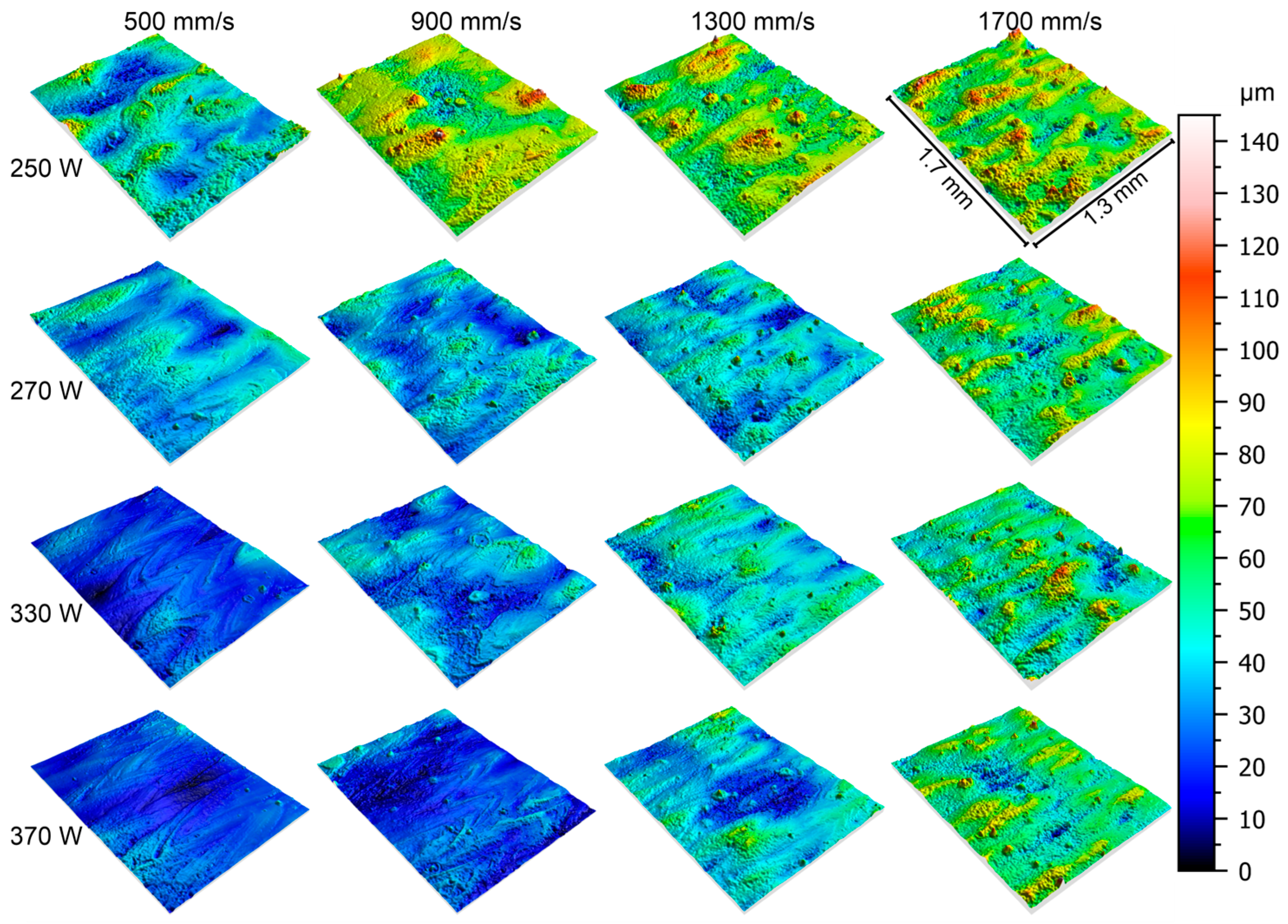
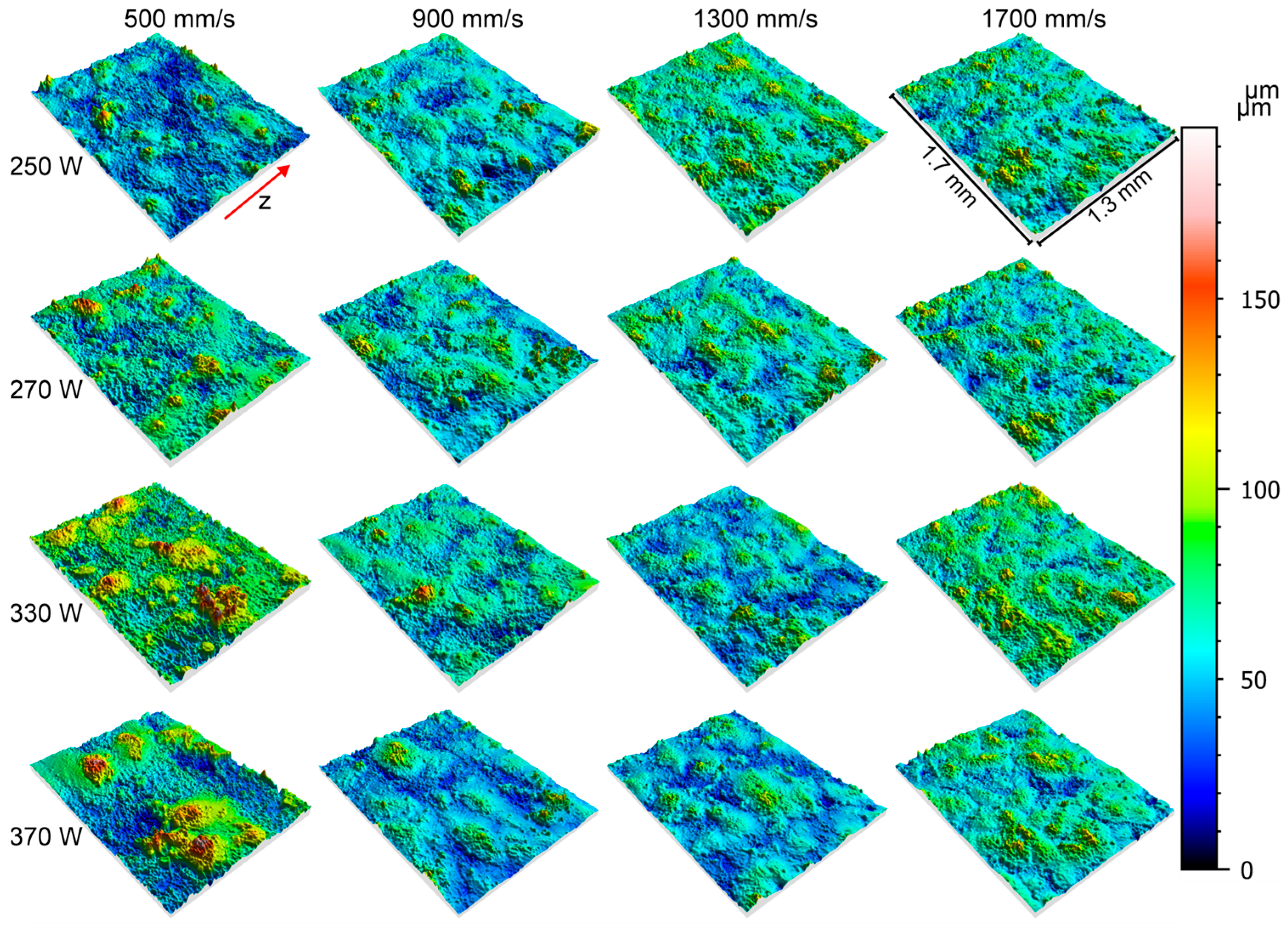
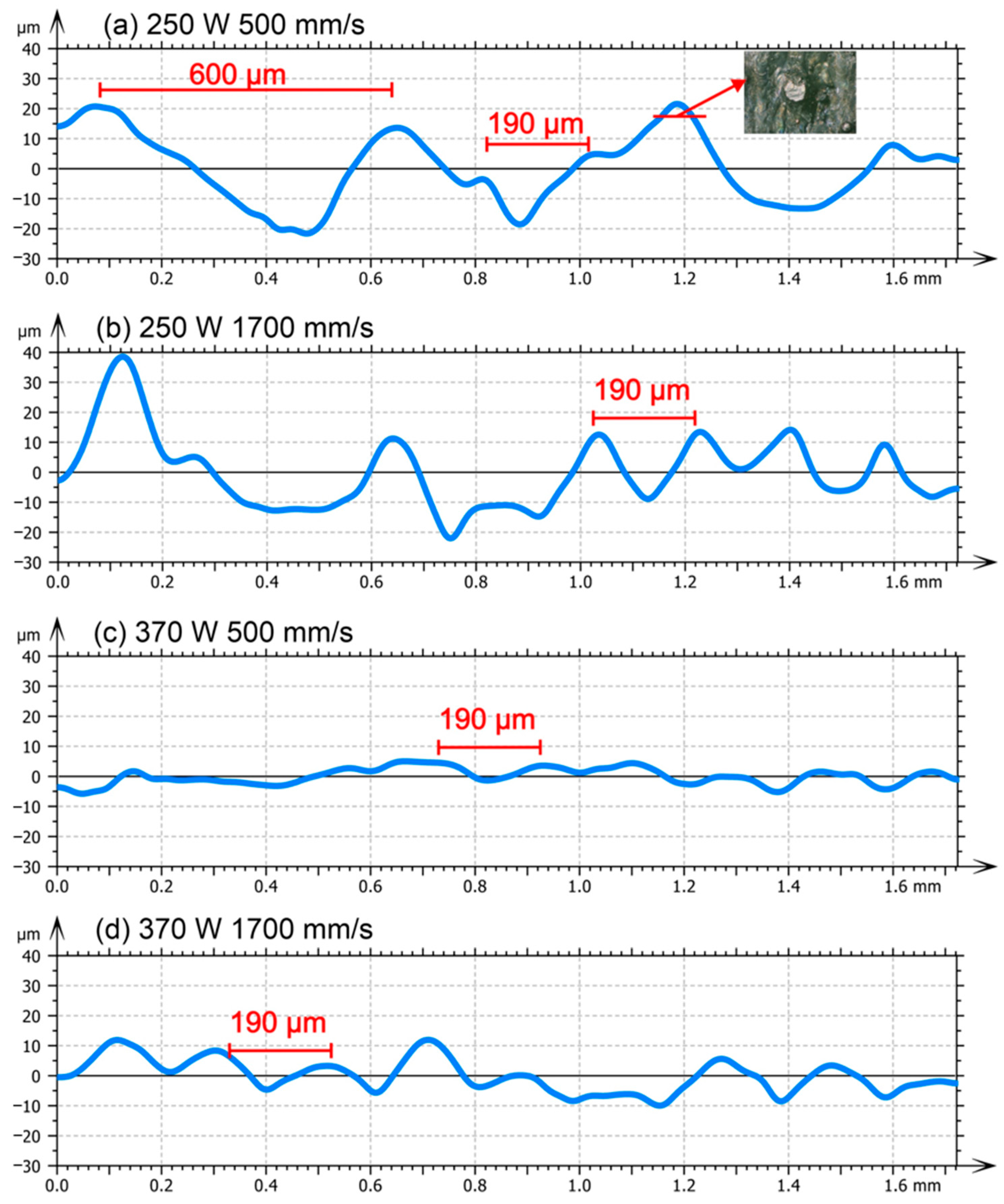
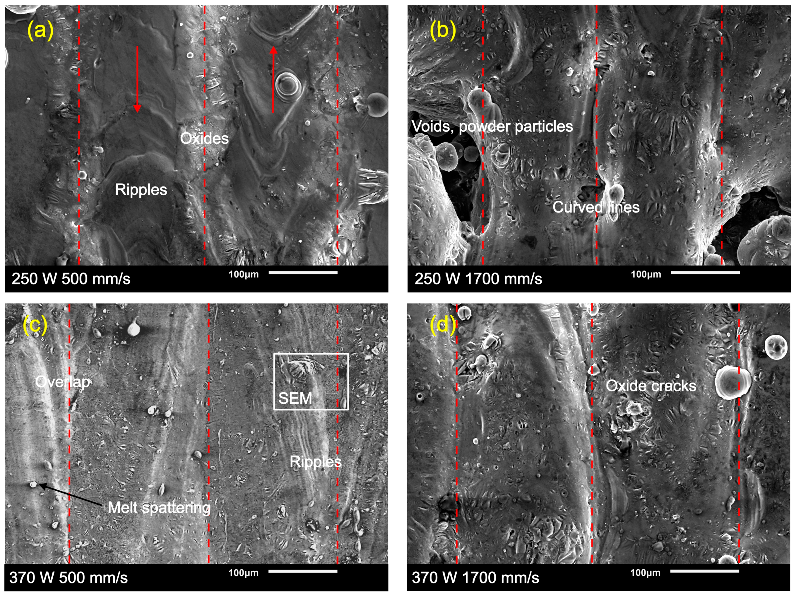
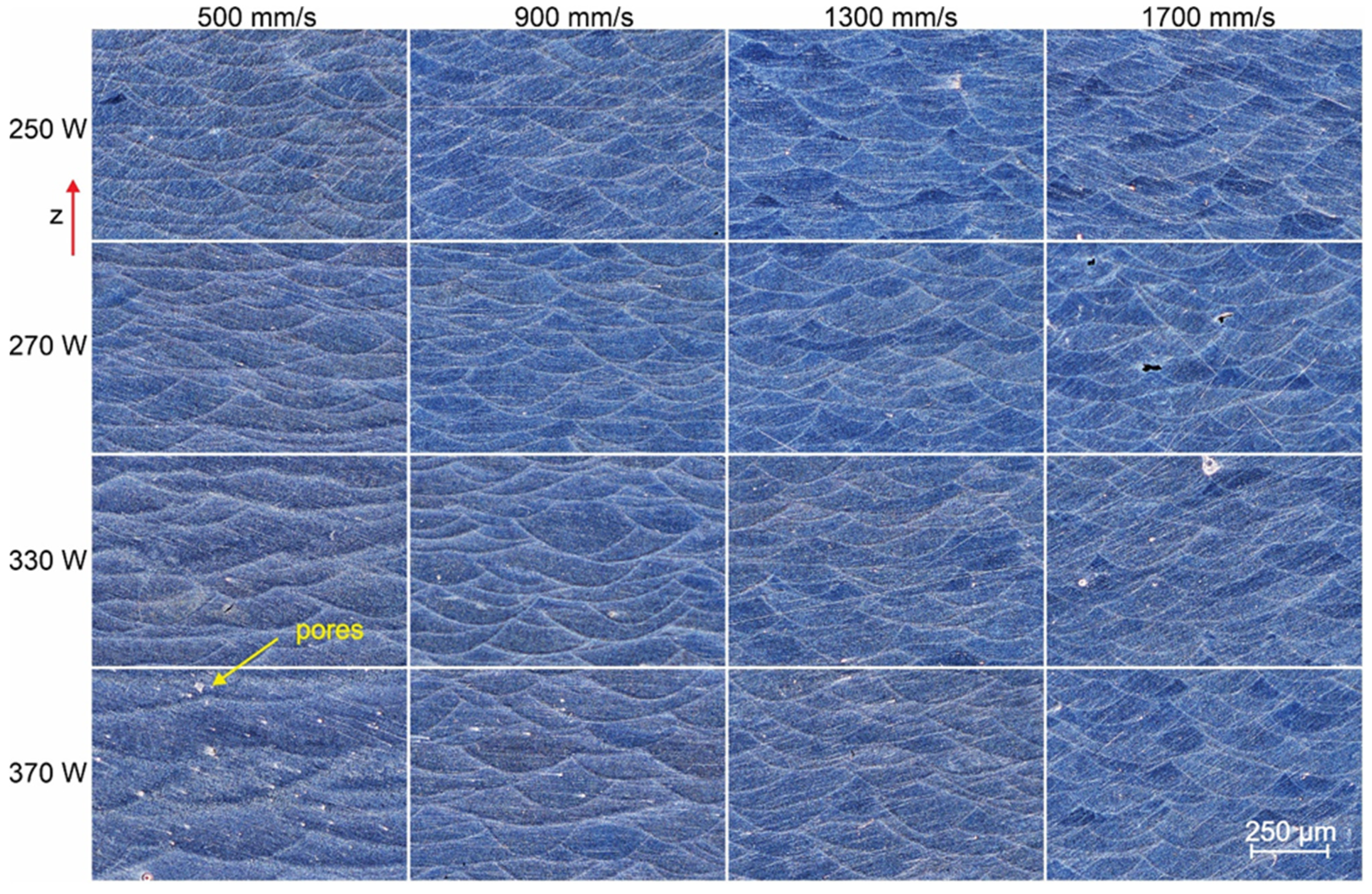
3.1. Topography
3.2. Surface Roughness
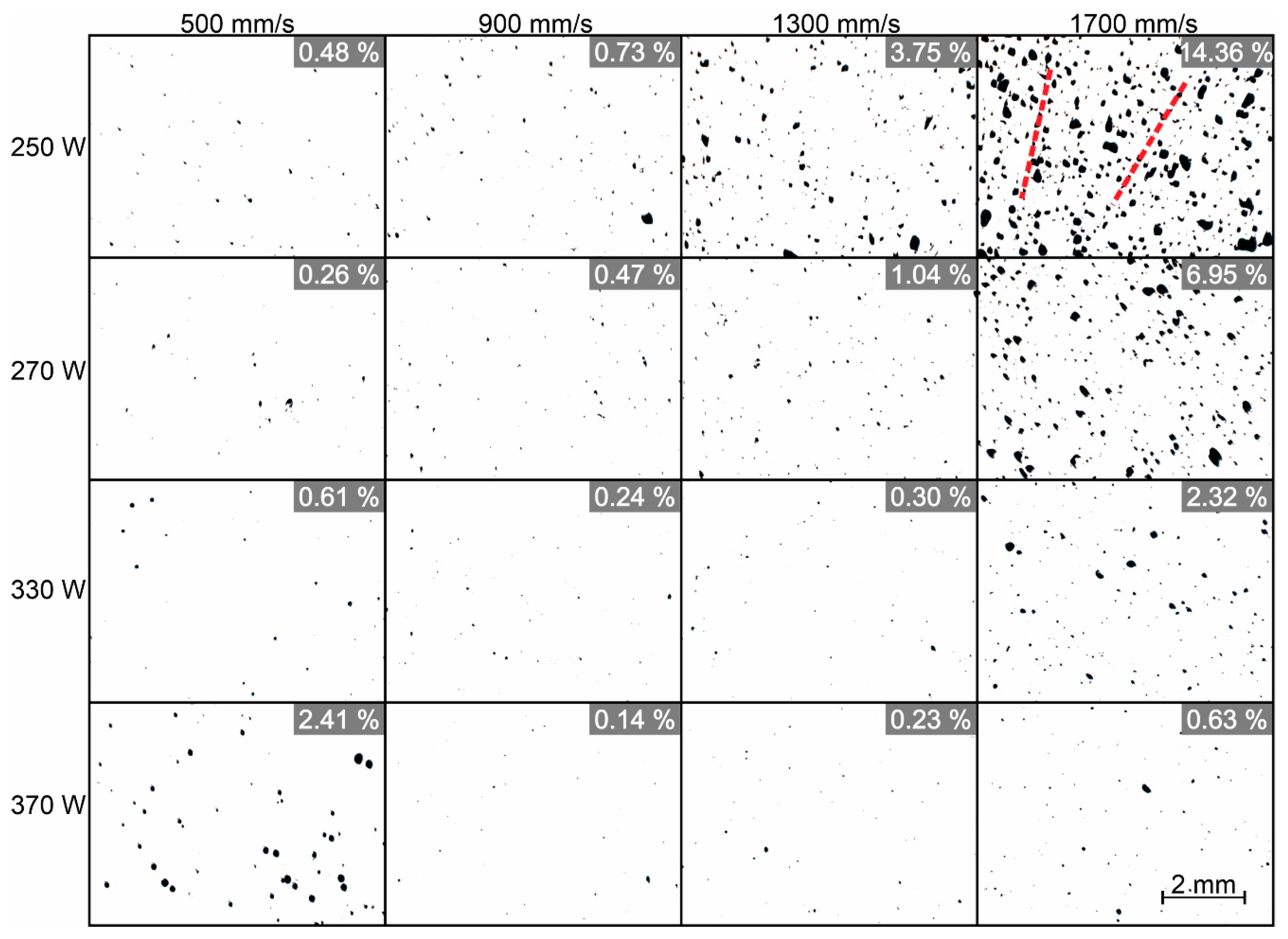
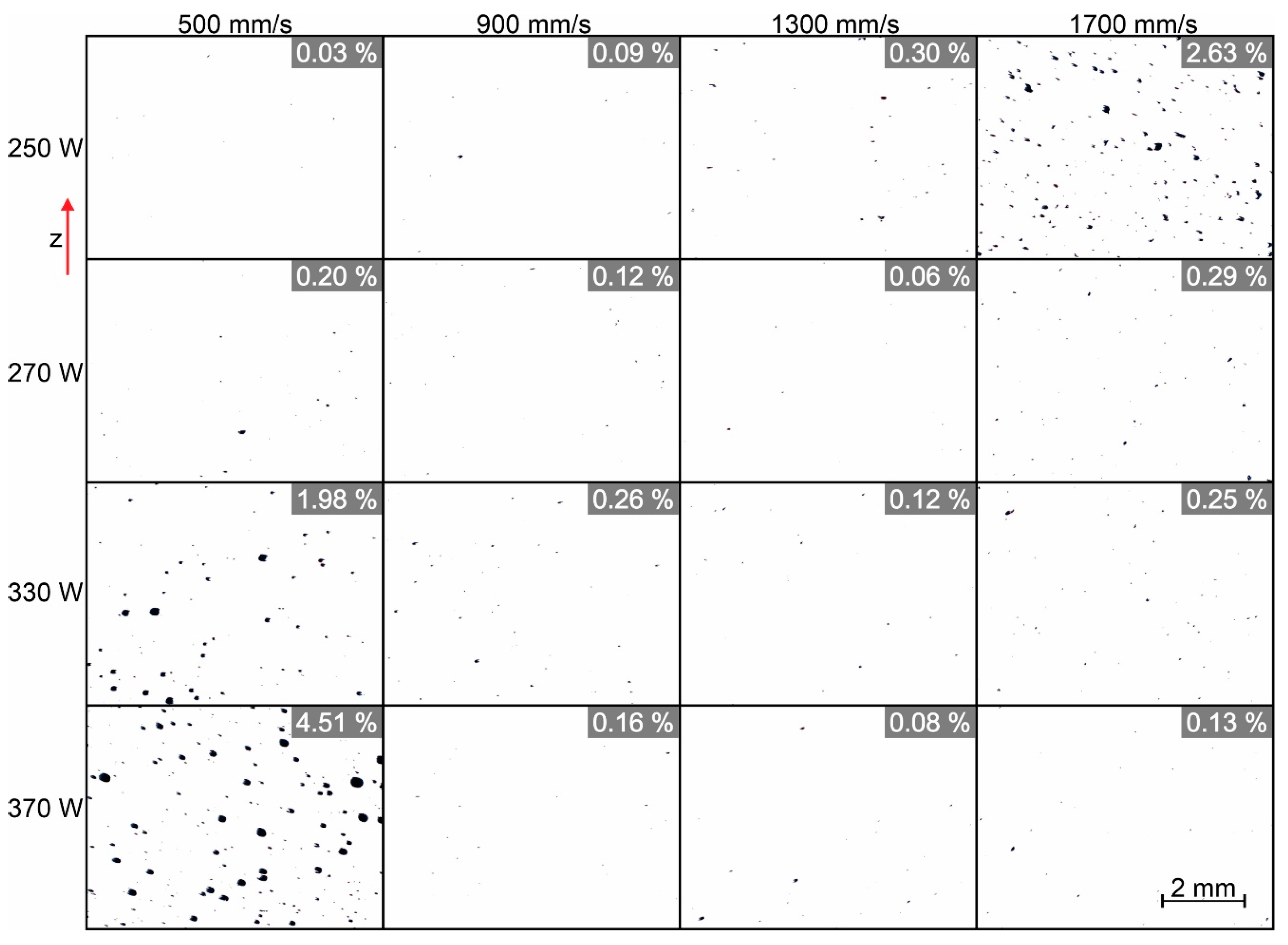
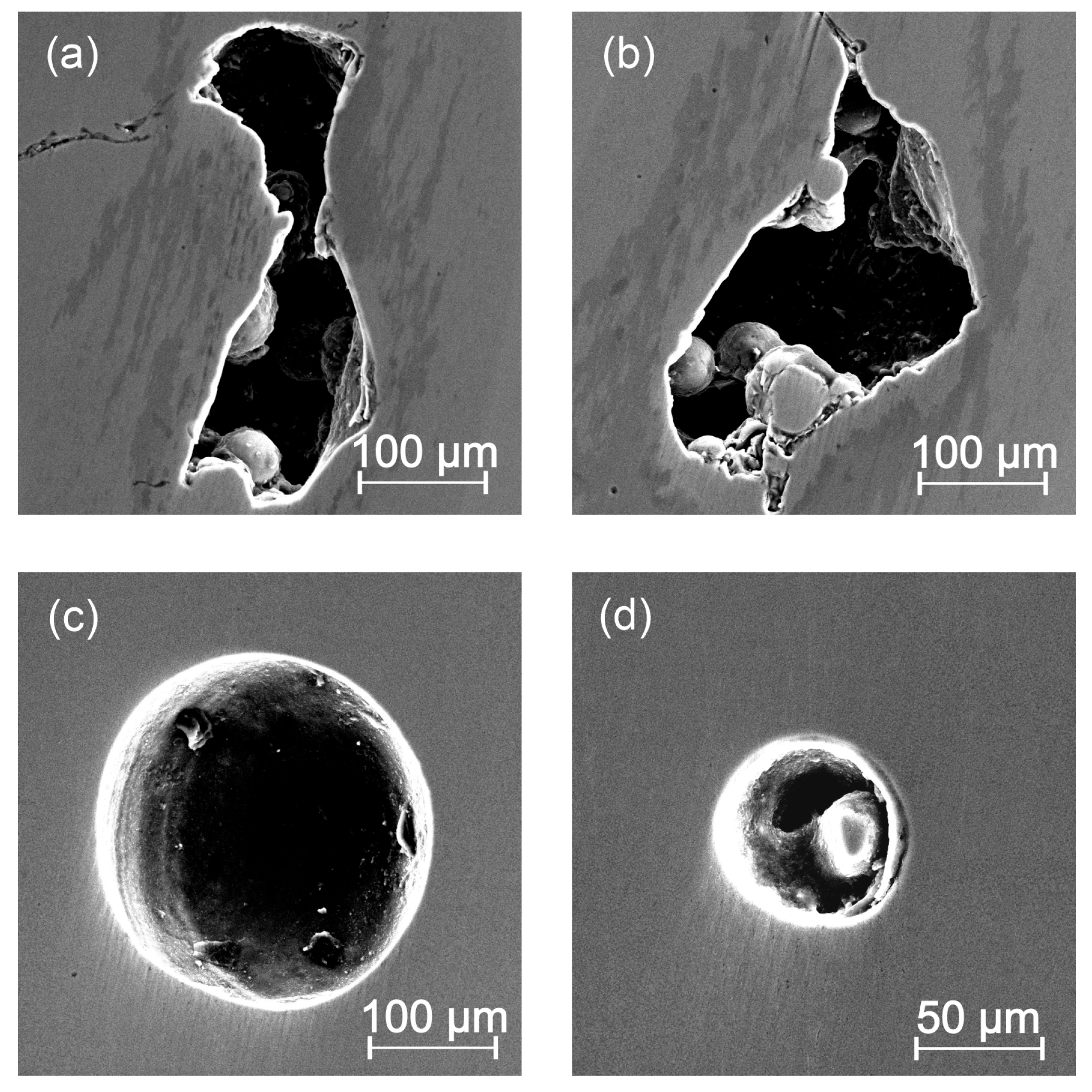
3.3. Surface Porosity
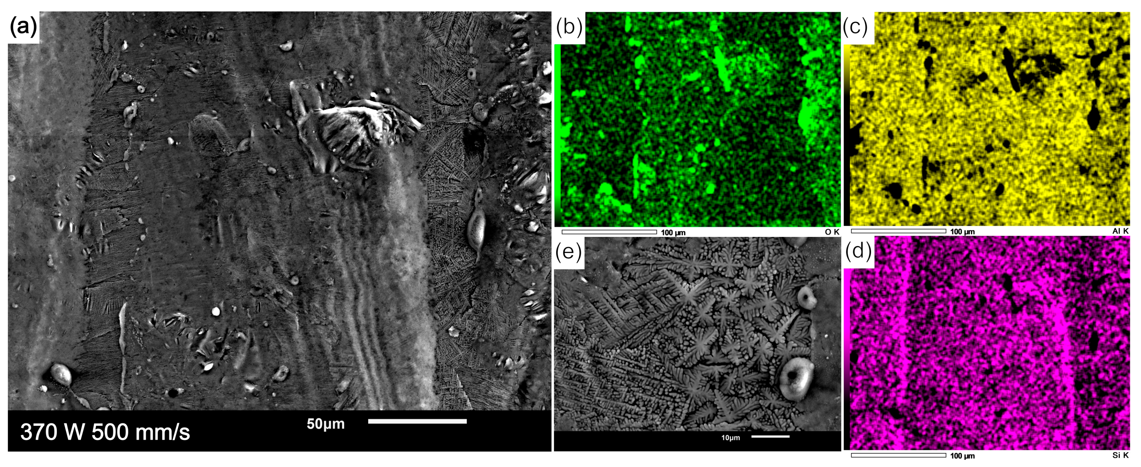
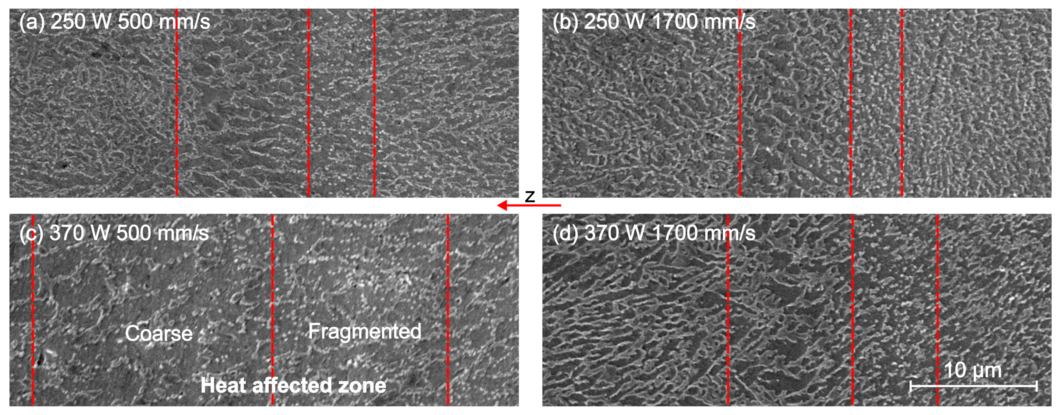
3.4. Microstructure
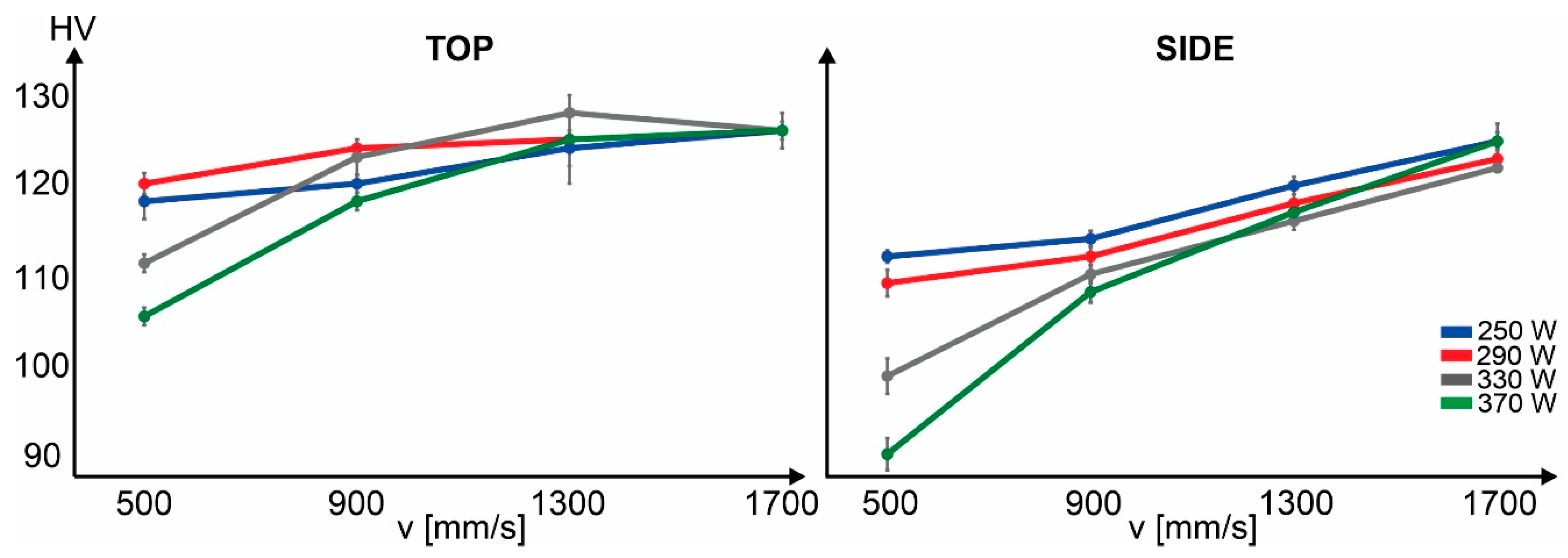
3.5. Hardness
4. Discussion
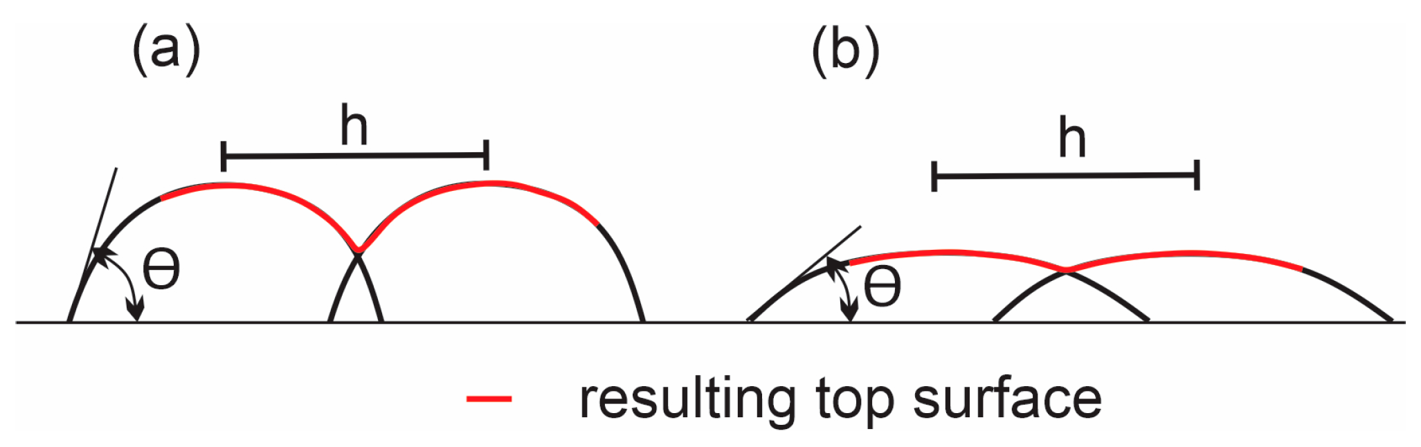
4.1. Effect of Processing Parameters on Topography
4.2. Topography Characterization Using Multiple Parameters
4.3. Effect of Processing Parameters on Porosity
4.4. Effect of Processing Parameters on Microstructure
4.5. Effect of Processing Parameters on Hardness
5. Conclusions
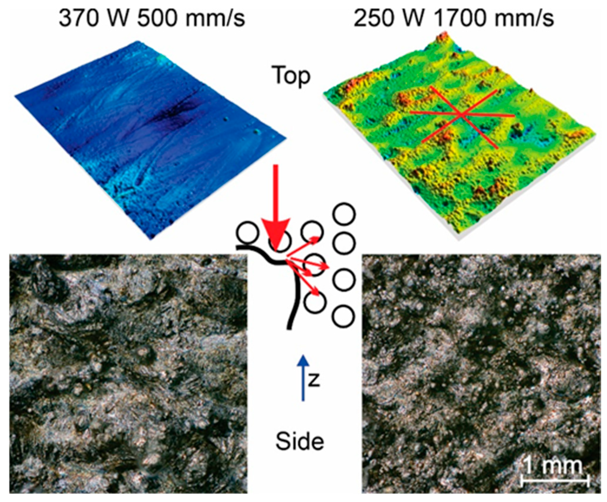
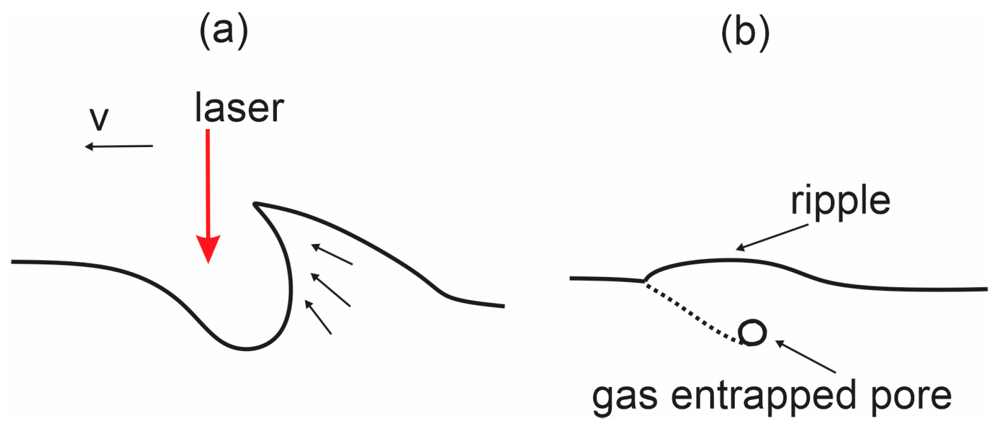
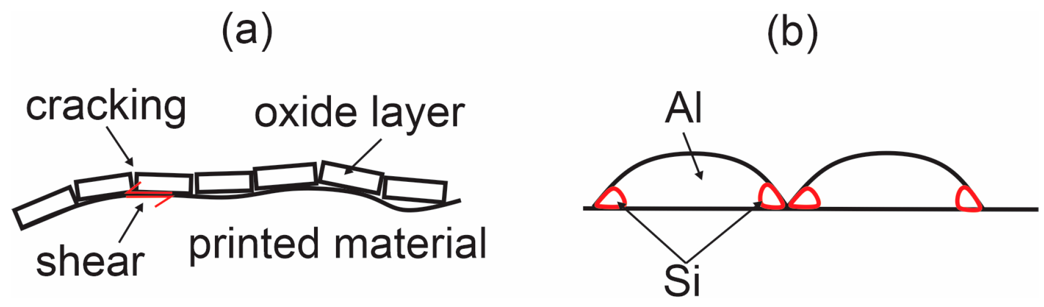
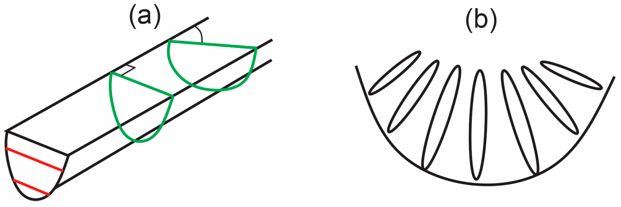
- With a high laser power and a slow scanning speed, top surfaces become flatter with more overlap due to sufficient spread of melt. With an increase in the scanning speed, scanned paths become more distinguished with increased height and with less power, the balling effect becomes predominant, causing waviness and larger gaps in between scanning lines. Side surfaces are mostly made up of adhered powder particles, caused by thermal conductivity or laser dispersion and are more predominant at lower energy densities.
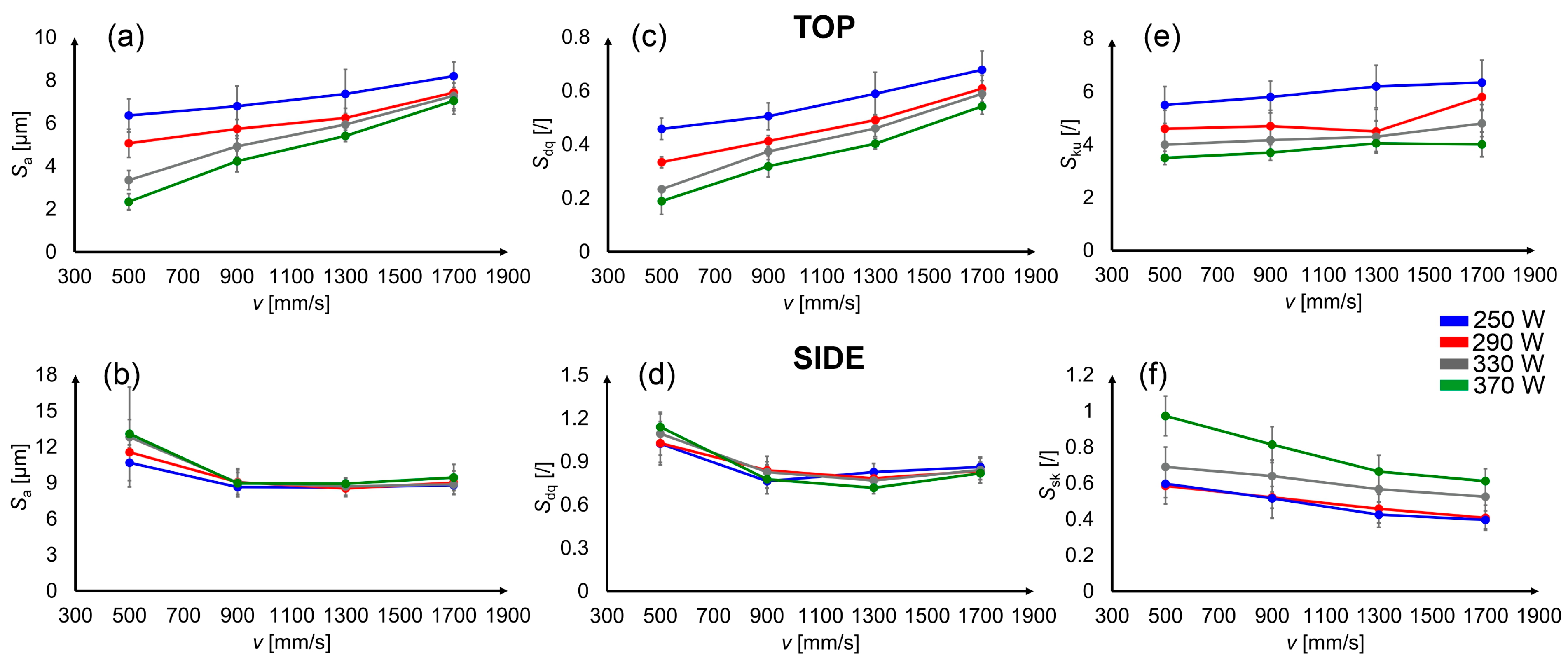
- The top surface roughness is, in general, three times lower than on the side surfaces, where a minimum Sa of 2.3 μm is achieved at 370 W and 500 mm/s for the top and 8.2 μm at 250 W 1300 mm/s on the side. With an increase in energy density, the roughness for top surfaces decreases, while for the side, it increases. Supplementary parameters of Sdq, Sku and Ssk can be used, to additionally describe the surface roughness and anisotropy.
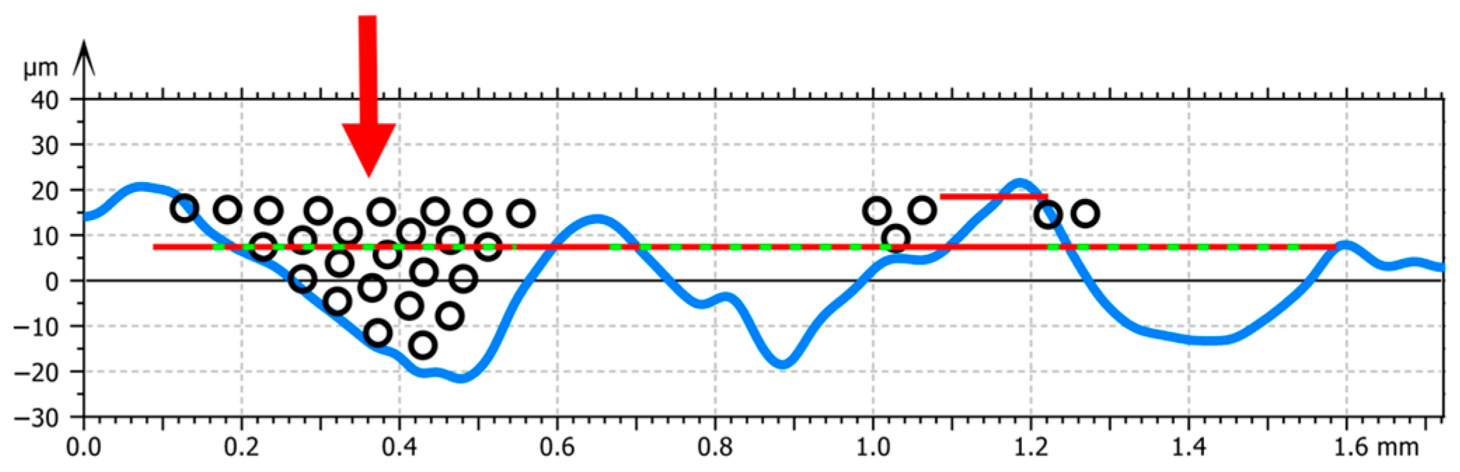
- The surface porosity of the printed specimens shows circular gas pores formed in the region at higher energy densities. On the other hand, a lack of fusion pores, with irregular shapes, filled with powder particles, are present at lower energy density. The porosity of the top surfaces is higher than that of the side surfaces, except in the gas-formed region of pores, where the porosity is higher on the side surfaces.
- The melt-pool geometry with an increase in the energy density is increasing, showing the orientation and scanning direction on the top surfaces and their cross-sections on the side surfaces. Additionally, the heat-affected zones at the boundaries comprise three regions, where the area is increasing with energy density. With a decrease in the energy density the cellular dendritic microstructure is becoming smaller. The side surfaces show the same type of heat-affected zones and size changes in the dendrites, but the dendrites have columnar geometries instead of cellular.
- The hardness mostly depends on the geometry of cell dendrites, which are affected by cooling rates. At low scanning speeds and high laser powers, the cooling rate is slower and the cell size increases, therefore reducing the hardness. With an increase in the scanning speed, the cells become finer and the hardness is increased, but this is limited by the higher porosity, especially at lower laser powers. On the other hand, side surfaces have a lower hardness due to the larger columnar size of the dendrites, but have less surface porosity, and therefore the hardness is constantly increasing even at lower energy densities.
- By using ANOVA analyses it was found that scanning speed consistently and strongly affects surface roughness on both top and side surfaces, while laser power plays a significant role only on the top surface. Porosity, however, does not show a clear linear relation to laser speed or power, but it has probably more complex behaviors.
Author Contributions
Funding
Data Availability Statement
Conflicts of Interest
Abbreviations
| AM | Additive manufacturing |
References
- Miao, G.; Moghadasi, M.; Li, M.; Pei, Z.; Ma, C. Binder Jetting Additive Manufacturing: Powder Packing in Shell Printing. J. Manuf. Mater. Process. 2022, 7, 4. [Google Scholar] [CrossRef]
- Wang, L.-Z.; Wang, S.; Wu, J.-J. Experimental investigation on densification behavior and surface roughness of AlSi10Mg powders produced by selective laser melting. Opt. Laser Technol. 2017, 96, 88–96. [Google Scholar] [CrossRef]
- Koutiri, I.; Pessard, E.; Peyre, P.; Amlou, O.; De Terris, T. Influence of SLM process parameters on the surface finish, porosity rate and fatigue behavior of as-built Inconel 625 parts. J. Mater. Process Technol. 2018, 255, 536–546. [Google Scholar] [CrossRef]
- Ngo, T.D.; Kashani, A.; Imbalzano, G.; Nguyen, K.T.Q.; Hui, D. Additive manufacturing (3D printing): A review of materials, methods, applications and challenges. Compos. B Eng. 2018, 143, 172–196. [Google Scholar] [CrossRef]
- Bajaj, P.; Hariharan, A.; Kini, A.; Kürnsteiner, P.; Raabe, D.; Jägle, E.A. Steels in additive manufacturing: A review of their microstructure and properties. Mater. Sci. Eng. A 2020, 772, 138633. [Google Scholar] [CrossRef]
- Simson, T.; Koch, J.; Rosenthal, J.; Kepka, M.; Zetek, M.; Zetková, I.; Wolf, G.; Tomčík, P.; Kulhánek, J. Mechanical Properties of 18Ni-300 maraging steel manufactured by LPBF. Procedia Struct. Integr. 2019, 17, 843–849. [Google Scholar] [CrossRef]
- Yan, Q.; Song, B.; Shi, Y. Comparative study of performance comparison of AlSi10Mg alloy prepared by selective laser melting and casting. J. Mater. Sci. Technol. 2020, 41, 199–208. [Google Scholar] [CrossRef]
- Chen, Y.; Chen, H.; Chen, J.; Xiong, J.; Wu, Y.; Dong, S. Numerical and experimental investigation on thermal behavior and microstructure during selective laser melting of high strength steel. J. Manuf. Process 2020, 57, 533–542. [Google Scholar] [CrossRef]
- Jia, H.; Sun, H.; Wang, H.; Wu, Y.; Wang, H. Scanning strategy in selective laser melting (SLM): A review. Int. J. Adv. Manuf. Technol. 2021, 113, 2413–2435. [Google Scholar] [CrossRef]
- Hadadzadeh, A.; Amirkhiz, B.S.; Langelier, B.; Li, J.; Mohammadi, M. Microstructural consistency in the additive manufactured metallic materials: A study on the laser powder bed fusion of AlSi10Mg. Addit. Manuf. 2021, 46, 102166. [Google Scholar] [CrossRef]
- Dursun, G.; Ibekwe, S.; Li, G.; Mensah, P.; Joshi, G.; Jerro, D. Influence of laser processing parameters on the surface characteristics of 316L stainless steel manufactured by selective laser melting. Mater. Today Proc. 2020, 26, 387–393. [Google Scholar] [CrossRef]
- Pisula, J.M.; Budzik, G.; Przeszłowski, Ł. An Analysis of the Surface Geometric Structure and Geometric Accuracy of Cylindrical Gear Teeth Manufactured with the Direct Metal Laser Sintering (DMLS) Method. Stroj. Vestn.-J. Mech. Eng. 2019, 65, 78–86. [Google Scholar] [CrossRef]
- Majeed, A.; Ahmed, A.; Salam, A.; Sheikh, M.Z. Surface quality improvement by parameters analysis, optimization and heat treatment of AlSi10Mg parts manufactured by SLM additive manufacturing. Int. J. Lightweight Mater. Manuf. 2019, 2, 288–295. [Google Scholar] [CrossRef]
- Yu, W.; Sing, S.L.; Chua, C.K.; Tian, X. Influence of re-melting on surface roughness and porosity of AlSi10Mg parts fabricated by selective laser melting. J. Alloys Compd. 2019, 792, 574–581. [Google Scholar] [CrossRef]
- Yang, T.; Liu, T.; Liao, W.; MacDonald, E.; Wei, H.; Chen, X.; Jiang, L. The influence of process parameters on vertical surface roughness of the AlSi10Mg parts fabricated by selective laser melting. J. Mater. Process Technol. 2019, 266, 26–36. [Google Scholar] [CrossRef]
- Balbaa, M.A.; Elbestawi, M.A.; McIsaac, J. An experimental investigation of surface integrity in selective laser melting of Inconel 625. Int. J. Adv. Manuf. Technol. 2019, 104, 3511–3529. [Google Scholar] [CrossRef]
- Kok, Y.; Tan, X.; Wang, P.; Nai, M.; Loh, N.; Liu, E.; Tor, S. Anisotropy and heterogeneity of microstructure and mechanical properties in metal additive manufacturing: A critical review. Mater. Des. 2018, 139, 565–586. [Google Scholar] [CrossRef]
- Lou, S.; Jiang, X.; Sun, W.; Zeng, W.; Pagani, L.; Scott, P. Characterisation methods for powder bed fusion processed surface topography. Precis. Eng. 2019, 57, 1–15. [Google Scholar] [CrossRef]
- Thompson, A.; Senin, N.; Giusca, C.; Leach, R. Topography of selectively laser melted surfaces: A comparison of different measurement methods. CIRP Ann. Manuf. Technol. 2017, 66, 543–546. [Google Scholar] [CrossRef]
- Aboulkhair, N.T.; Everitt, N.M.; Ashcroft, I.; Tuck, C. Reducing porosity in AlSi10Mg parts processed by selective laser melting. Addit. Manuf. 2014, 1, 77–86. [Google Scholar] [CrossRef]
- Majeed, A.; Zhang, Y.; Lv, J.; Peng, T.; Atta, Z.; Ahmed, A. Investigation of T4 and T6 heat treatment influences on relative density and porosity of AlSi10Mg alloy components manufactured by SLM. Comput. Ind. Eng. 2020, 139, 106194. [Google Scholar] [CrossRef]
- Gu, D.; Wang, H.; Chang, F.; Dai, D.; Yuan, P.; Hagedorn, Y.C.; Meiners, W. Selective laser melting additive manufacturing of TiC/AlSi10Mg bulk-form nanocomposites with tailored microstructures and properties. Phys. Procedia 2014, 56, 108–116. [Google Scholar] [CrossRef]
- Wu, L.; Zhao, Z.; Bai, P.; Zhao, W.; Li, Y.; Liang, M.; Liao, H.; Huo, P.; Li, J. Wear resistance of graphene nano-platelets (GNPs) reinforced AlSi10Mg matrix composite prepared by SLM. Appl. Surf. Sci. 2020, 503, 144156. [Google Scholar] [CrossRef]
- Liu, Y.; Liu, Z.; Jiang, Y.; Wang, G.; Yang, Y.; Zhang, L. Gradient in microstructure and mechanical property of selective laser melted AlSi10Mg. J. Alloys Compd. 2018, 735, 1414–1421. [Google Scholar] [CrossRef]
- Zhou, L.; Mehta, A.; Schulz, E.; McWilliams, B.; Cho, K.; Sohn, Y. Microstructure, precipitates and hardness of selectively laser melted AlSi10Mg alloy before and after heat treatment. Mater. Charact. 2018, 143, 5–17. [Google Scholar] [CrossRef]
- Iturrioz, A.; Gil, E.; Petite, M.M.; Garciandia, F.; Mancisidor, A.M.; Sebastian, M.S. Selective laser melting of AlSi10Mg alloy: Influence of heat treatment condition on mechanical properties and microstructure. Weld. World 2018, 62, 885–892. [Google Scholar] [CrossRef]
- Li, W.; Li, S.; Liu, J.; Zhang, A.; Zhou, Y.; Wei, Q.; Yan, C.; Shi, Y. Effect of heat treatment on AlSi10Mg alloy fabricated by selective laser melting: Microstructure evolution, mechanical properties and fracture mechanism. Mater. Sci. Eng. A 2016, 663, 116–125. [Google Scholar] [CrossRef]
- Ghasri-Khouzani, M.; Peng, H.; Attardo, R.; Ostiguy, P.; Neidig, J.; Billo, R.; Hoelzle, D.; Shankar, M. Comparing microstructure and hardness of direct metal laser sintered AlSi10Mg alloy between different planes. J. Manuf. Process 2019, 37, 274–280. [Google Scholar] [CrossRef]
- Chen, J.; Hou, W.; Wang, X.; Chu, S.; Yang, Z. Microstructure, porosity and mechanical properties of selective laser melted AlSi10Mg. Chin. J. Aeronaut. 2020, 33, 2043–2054. [Google Scholar] [CrossRef]
- Girelli, L.; Tocci, M.; Montesano, L.; Gelfi, M.; Pola, A. Optimization of heat treatment parameters for additive manufacturing and gravity casting AlSi10Mg alloy. IOP Conf. Ser. Mater. Sci. Eng. 2017, 264, 12016. [Google Scholar] [CrossRef]
- Available online: https://store.eos.info/products/eos-aluminum-alsi10mg (accessed on 13 June 2025).
- ISO 25178-2:2012; Geometrical Product Specifications (GPS)—Surface Texture: Areal—Part 2: Terms, Definitions and Surface Texture Parameters. International Organization for Standardization (ISO): Geneva, Switzerland, 2012.
- Zhu, Y.; Chen, X.; Zou, J.; Yang, H. Sliding wear of selective laser melting processed Ti6Al4V under boundary lubrication conditions. Wear 2016, 368–369, 485–495. [Google Scholar] [CrossRef]
- Liu, S.; Guo, H. Balling behavior of selective laser melting (SLM) magnesium alloy. Materials 2020, 13, 3632. [Google Scholar] [CrossRef] [PubMed]
- Shi, Q.; Gu, D.; Xia, M.; Cao, S.; Rong, T. Effects of laser processing parameters on thermal behavior and melting/solidification mechanism during selective laser melting of TiC/Inconel 718 composites. Opt. Laser Technol. 2016, 84, 9–22. [Google Scholar] [CrossRef]
- Maamoun, A.H.; Xue, Y.F.; Elbestawi, M.A.; Veldhuis, S.C. Effect of selective laser melting process parameters on the quality of al alloy parts: Powder characterization, density, surface roughness, and dimensional accuracy. Materials 2018, 11, 2343. [Google Scholar] [CrossRef]
- Maamoun, A.H.; Xue, Y.F.; Elbestawi, M.A.; Veldhuis, S.C. The effect of selective laser melting process parameters on the microstructure and mechanical properties of Al6061 and AlSi10Mg alloys. Materials 2019, 12, 12. [Google Scholar] [CrossRef]
- Masiagutova, E.; Cabanettes, F.; Sova, A.; Cici, M.; Bidron, G.; Bertrand, P. Side surface topography generation during laser powder bed fusion of AlSi10Mg. Addit. Manuf. 2021, 47, 102230. [Google Scholar] [CrossRef]
- Raza, A.; Fiegl, T.; Hanif, I.; Markström, A.; Franke, M.; Körner, C.; Hryha, E. Degradation of AlSi10Mg powder during laser based powder bed fusion processing. Mater. Des. 2021, 198, 109358. [Google Scholar] [CrossRef]
- Han, X.; Zhu, H.; Nie, X.; Wang, G.; Zeng, X. Investigation on selective laser melting AlSi10Mg cellular lattice strut: Molten pool morphology, surface roughness and dimensional accuracy. Materials 2018, 11, 392. [Google Scholar] [CrossRef]
- Gu, D.; Wang, H.; Dai, D.; Chang, F.; Meiners, W.; Hagedorn, Y.-C.; Wissenbach, K.; Kelbassa, I.; Poprawe, R. Densification behavior, microstructure evolution, and wear property of TiC nanoparticle reinforced AlSi10Mg bulk-form nanocomposites prepared by selective laser melting. J. Laser Appl. 2015, 27, S17003. [Google Scholar] [CrossRef]
- Dai, D.; Gu, D. Effect of metal vaporization behavior on keyhole-mode surface morphology of selective laser melted composites using different protective atmospheres. Appl. Surf. Sci. 2015, 355, 310–319. [Google Scholar] [CrossRef]
- Tang, P.; Wang, S.; Duan, H.; Long, M.; Li, Y.; Fan, S.; Chen, D. The Formation of Humps and Ripples During Selective Laser Melting of 316l Stainless Steel. Jom 2020, 72, 1128–1137. [Google Scholar] [CrossRef]
- Hu, J.; Guo, H.; Tsai, H.L. Weld pool dynamics and the formation of ripples in 3D gas metal arc welding. Int. J. Heat. Mass. Transf. 2008, 51, 2537–2552. [Google Scholar] [CrossRef]
- Cao, L. Mesoscopic-Scale Numerical Simulation Including the Influence of Process Parameters on SLM Single-Layer Multi-pass Formation. Metall. Mater. Trans. A Phys. Metall. Mater. Sci. 2020, 51, 4130–4145. [Google Scholar] [CrossRef]
- Tang, C.; Le, K.Q.; Wong, C.H. Physics of humping formation in laser powder bed fusion. Int. J. Heat Mass Transf. 2020, 149, 119172. [Google Scholar] [CrossRef]
- Nychka, J.A.; Pullen, C.; He, M.Y.; Clarke, D.R. Surface oxide cracking associated with oxidation-induced grain boundary sliding in the underlying alloy. Acta Mater. 2004, 52, 1097–1105. [Google Scholar] [CrossRef]
- Mehrabian, M.; Nayebi, B.; Bahmani, A.; Dietrich, D.; Lampke, T.; Ahounbar, E.; Shokouhimehr, M. Deformation, Cracking and Fracture Behavior of Dynamically-Formed Oxide Layers on Molten Metals. Met. Mater. Int. 2021, 27, 1701–1712. [Google Scholar] [CrossRef]
- Dai, D.; Gu, D.; Xia, M.; Ma, C.; Chen, H.; Zhao, T.; Hong, C.; Gasser, A.; Poprawe, R. Melt spreading behavior, microstructure evolution and wear resistance of selective laser melting additive manufactured AlN/AlSi10Mg nanocomposite. Surf. Coat. Technol. 2018, 349, 279–288. [Google Scholar] [CrossRef]
- Charles, A.P.; Elkaseer, A.; Thijs, L.; Hagenmeyer, V.; Scholz, S. Effect of process parameters on the generated surface roughness of down-facing surfaces in selective laser melting. Appl. Sci. 2019, 9, 1256. [Google Scholar] [CrossRef]
- Tempelman, J.R.; Wachtor, A.J.; Flynn, E.B.; Depond, P.J.; Forien, J.-B.; Guss, G.M.; Calta, N.P.; Matthews, M.J. Detection of keyhole pore formations in laser powder-bed fusion using acoustic process monitoring measurements. Addit. Manuf. 2022, 55, 102735. [Google Scholar] [CrossRef]
- Hu, Z.; Nagarajan, B.; Song, X.; Huang, R.; Zhai, W.; Wei, J. Formation of SS316L Single Tracks in Micro Selective Laser Melting: Surface, Geometry, and Defects. Adv. Mater. Sci. Eng. 2019, 2019, 9451406. [Google Scholar] [CrossRef]
- Gu, D.; Shi, Q.; Lin, K.; Xi, L. Microstructure and performance evolution and underlying thermal mechanisms of Ni-based parts fabricated by selective laser melting. Addit. Manuf. 2018, 22, 265–278. [Google Scholar] [CrossRef]
- Tezel, T.; Topal, E.S.; Kovan, V. Characterising the wear behaviour of DMLS-manufactured gears under certain operating conditions. Wear 2019, 440–441, 203106. [Google Scholar] [CrossRef]
- Rathod, H.J.; Nagaraju, T.; Prashanth, K.G.; Ramamurty, U. Tribological properties of selective laser melted Al–12Si alloy. Tribol. Int. 2019, 137, 94–101. [Google Scholar] [CrossRef]


| Sample No. | Laser Power [W] | Scanning Speed [mm/s] | Energy Density, η [J/mm3] |
|---|---|---|---|
| 1 | 250 | 500 | 88 |
| 2 | 250 | 900 | 49 |
| 3 | 250 | 1300 | 34 |
| 4 | 250 | 1700 | 26 |
| 5 | 290 | 500 | 102 |
| 6 | 290 | 900 | 57 |
| 7 | 290 | 1300 | 39 |
| 8 | 290 | 1700 | 30 |
| 9 | 330 | 500 | 116 |
| 10 | 330 | 900 | 64 |
| 11 | 330 | 1300 | 45 |
| 12 | 330 | 1700 | 34 |
| 13 | 370 | 500 | 130 |
| 14 | 370 | 900 | 72 |
| 15 | 370 | 1300 | 50 |
| 16 | 370 | 1700 | 38 |
| Variable | SS | DoF | MS | F | p-Value | F-crit |
|---|---|---|---|---|---|---|
| TOP SURFACE | ||||||
| Laser power | 13.05 | 3 | 4.35 | 13.22 | 0.00119 | 3.86 |
| Scanning speed | 21.93 | 3 | 7.31 | 22.22 | 0.00017 | 3.86 |
| Error | 2.96 | 9 | 0.33 | |||
| SIDE SURFACE | ||||||
| Laser power | 1.88 | 3 | 0.62 | 2.41 | 0.13375 | 3.86 |
| Scanning speed | 30.03 | 3 | 10.01 | 38.50 | 1.8 × 10⁻⁵ | 3.86 |
| Error | 2.34 | 9 | 0.26 |
| Variable | SS | DoF | MS | F | p-Value | F-crit |
|---|---|---|---|---|---|---|
| TOP SURFACE | ||||||
| Laser power | 42.03 | 3 | 14.01 | 1.53 | 0.27291 | 3.86 |
| Scanning speed | 82.16 | 3 | 27.39 | 2.99 | 0.08844 | 3.86 |
| Error | 82.49 | 9 | 9.17 | |||
| SIDE SURFACE | ||||||
| Laser power | 2.24 | 3 | 0.75 | 0.44 | 0.72821 | 3.86 |
| Scanning speed | 6.34 | 3 | 2.11 | 1.25 | 0.34755 | 3.86 |
| Error | 15.18 | 9 | 1.69 |
Disclaimer/Publisher’s Note: The statements, opinions and data contained in all publications are solely those of the individual author(s) and contributor(s) and not of MDPI and/or the editor(s). MDPI and/or the editor(s) disclaim responsibility for any injury to people or property resulting from any ideas, methods, instructions or products referred to in the content. |
© 2025 by the authors. Licensee MDPI, Basel, Switzerland. This article is an open access article distributed under the terms and conditions of the Creative Commons Attribution (CC BY) license (https://creativecommons.org/licenses/by/4.0/).
Share and Cite
Klanjšček, U.; Kalin, M. Analysis of the Topographical, Microstructural and Mechanical Surface Properties of Powder Bed Fusion Melted AlSi10Mg for a Broad Range of Process Parameters. J. Manuf. Mater. Process. 2025, 9, 200. https://doi.org/10.3390/jmmp9060200
Klanjšček U, Kalin M. Analysis of the Topographical, Microstructural and Mechanical Surface Properties of Powder Bed Fusion Melted AlSi10Mg for a Broad Range of Process Parameters. Journal of Manufacturing and Materials Processing. 2025; 9(6):200. https://doi.org/10.3390/jmmp9060200
Chicago/Turabian StyleKlanjšček, Urban, and Mitjan Kalin. 2025. "Analysis of the Topographical, Microstructural and Mechanical Surface Properties of Powder Bed Fusion Melted AlSi10Mg for a Broad Range of Process Parameters" Journal of Manufacturing and Materials Processing 9, no. 6: 200. https://doi.org/10.3390/jmmp9060200
APA StyleKlanjšček, U., & Kalin, M. (2025). Analysis of the Topographical, Microstructural and Mechanical Surface Properties of Powder Bed Fusion Melted AlSi10Mg for a Broad Range of Process Parameters. Journal of Manufacturing and Materials Processing, 9(6), 200. https://doi.org/10.3390/jmmp9060200