Article

Optimizing the Die-Sink EDM Machinability of AISI 316L Using Ti-6Al-4V-SiCp Electrodes: A Computational Approach

Department of Mechanical and Industrial Engineering, Manipal Institute of Technology, Manipal Academy of Higher Education, Manipal, Udupi 576104, India
*
Authors to whom correspondence should be addressed.
J. Manuf. Mater. Process. 2024, 8(5), 202; https://doi.org/10.3390/jmmp8050202
Submission received: 14 August 2024 / Revised: 12 September 2024 / Accepted: 16 September 2024 / Published: 18 September 2024

Abstract

:
Die-sink electric discharge machining (EDM) is essential for shaping complex geometries in hard-to-machine materials. This study aimed to optimize key input parameters, such as the discharge current, gap voltage, pulse-on time, and pulse-off time, to enhance the EDM performance by maximizing the material removal rate while minimizing the surface roughness, residual stress, microhardness, and recast layer thickness. AISI 316L stainless steel was chosen due to its industrial relevance and machining challenges, while a Ti-6Al-4V-SiCp composite electrode was selected for its thermal resistance and low wear. Using Taguchi’s L27 orthogonal array, this study minimized the trial numbers, with analysis of the variance-quantifying parameter contributions. The results showed a maximum material removal rate of 0.405 g/min and minimal values for the surface roughness (1.95 µm), residual stress (1063.74 MPa), microhardness (244.8 Hv), and recast layer thickness (0.47 µm). A second-order model, developed through a response surface methodology, and a feed-forward artificial neural network enhanced the prediction accuracy. Multi-response optimization using desirability function analysis yielded an optimal set of conditions: discharge current of 5.78 amperes, gap voltage of 90 volts, pulse-on time of 100 microseconds, and pulse-off time of 15 microseconds. This setup achieved a material removal rate of 0.13 g/min, with reduced surface roughness (2.46 µm), residual stress (1518.46 MPa), microhardness (259.01 Hv), and recast layer thickness (0.87 µm). Scanning electron microscopy further analyzed the surface morphology and recast layer characteristics, providing insights into the material behavior under EDM. These findings enhance the understanding and optimization of the EDM processes for challenging materials, offering valuable guidance for future research and industrial use.

1. Introduction

In recent days, die-sink electric discharge machining (EDM), also called volume EDM, has gained a lot of attention in terms of precision machining technology. Unlike traditional methods, which primarily rely on mechanical forces for material removal, EDM utilizes electrical discharges by eroding the workpiece irrespective of its hardness [1,2]. This has proved advantageous in creating intricate details and complex geometries with impeccable precision, which would be difficult with conventional machining operations [3]. The EDM processes can achieve high tolerances in the micrometer range and a high surface finish that seldom requires post-machining treatments. This is critical when producing dies and molds where the dimensional accuracy and surface integrity can directly influence the quality of the final product. Further, the process is highly versatile and used for applications ranging from micro components to large complex parts [4]. In die-sink EDM, the removal of material from the workpiece involves generating controlled electrical discharges between the workpiece and the tool electrode (Figure 1). This causes the localized melting and vaporization (formation of micro-craters) of the workpiece material, which is further washed away by the stream of dielectric fluid [5,6]. The electrode material composition effects the material removal rate [7,8]. While highly conductive materials like copper and graphite result in efficient spark generation, high melting point materials like tungsten sustain high intensity discharges, resulting in minimal wear. A delicate balance between both ensures efficient machining, resulting in high material removal rates and low electrode wear and surface roughness [8]. In die-sink EDM, the discharge current, also known as the peak current, has been found to be the most influential parameter effecting the material removal rate (MRR), surface roughness (SR), residual stresses (RS) and recast layer thickness (RLT). The discharge current determines the energy of the electrical discharges, thus resulting in greater material erosion per discharge as it is increased [9,10]. Further, the voltage applied across the electrode gap, known as the gap voltage, significantly influences the MRR. Higher gap voltages can facilitate a more stable discharge environment, resulting in consistent spark generation and efficient material removal [11,12,13,14]. Finally, the pulse-on and pulse-off times affect the MRR by dictating the time of energy delivery during each discharge. With longer pulse-on times and shorter pulse-off times, more energy is transferred, thus increasing the volume of material removal per pulse [15,16,17,18]. However, this must be carefully balanced in order to avoid excessive heat generation, which can deteriorate the surface quality and increase the electrode wear. The surface roughness is a crucial aspect of die-sink EDM as it directly influences the integrity of the final product. Lower discharge currents produce finer, more controlled discharges, leading to the generation of smaller craters on the workpiece surface [19,20,21]. This results in decreased surface roughness as the energy involved is less intense and the material removal occurs in a precise manner. Further, an increase in the pulse-on time, the duration each discharge is active, causes a uniform increase in the surface roughness as longer pulses allow more energy to be transferred to the workpiece [22,23,24,25]. Additionally, the hardness of workpieces also affects the roughness of the surface significantly. Harder materials tend to resist erosion more effectively, leading to smaller and less pronounced craters during machining, thus demanding the careful selection of the input process parameters while machining difficult-to-cut materials [26,27,28]. The internal stresses that remain in a workpiece after the external forces or thermal effects have been removed are known as residual stresses. In die-sink EDM, the residual stresses are mainly caused by the rapid thermal cycles of heating and cooling that occur during the machining process [29,30,31,32]. Higher discharge currents lead to intense spark generation, resulting in greater localized heating [33]. This leads to the formation of larger thermal gradients during the rapid cooling phase, resulting in higher residual stresses [34]. The increased energy discharge is the main reason for the intense melting and resolidification, which further intensifies the tensile residual stresses on the surface due to the shrinkage of the solidified layer [35]. Similarly, higher gap voltages can lead to more stable discharges but also to the energy delivered per discharge, resulting in more pronounced thermal cycling [36,37]. During the EDM process, each electrical discharge generates intense localized heating, causing the material to melt and vaporize. When the discharge stops, the molten material rapidly cools and solidifies. If the dielectric fluid stream is ineffective in flushing the recast layer, it significantly affects the final product, as it is often harder and more brittle than the workpiece [38,39,40,41,42,43]. The presence of the recast layer also negatively impacts the surface finish, resulting in micro-cracks and rough surfaces. Further, the brittleness and the residual stresses in the recast layer can reduce the fatigue strength and wear resistance of the product [44]. Finally, in applications requiring coating or bonding, the recast layer may affect the adhesion, leading to the poor coating performance or strength of the bond [45]. Higher peak currents result in more intense discharges, leading to the production of larger volumes of molten material, thus increasing the recast layer thickness. Conversely, lower gap voltages reduce the discharge energy, resulting in a thinner recast layer [46,47].
Taguchi’s design of experiments (DoE) is a statistical methodology designed to improve the efficiency and effectiveness of experimental findings. It can significantly reduce the number of experiments required to identify optimal conditions and analyze the effects of multiple parameters simultaneously [48]. To further enhance the analytical capabilities of the TDOE, various techniques, like the gray relation analysis (GRA), technique for order of preference by similarity to ideal solution (TOPSIS) and response surface methodology (RSM), can be integrated [48]. Out of these, the RSM is used for modeling and analyzing problems where multiple variables influence the response. By fitting a polynomial model to the experimental data, the RSM can predict the responses over a continuous range of parameter settings. When combined with the TDOE, the RSM allows for a detailed exploration of the response surface, leading to the identification of optimal conditions with greater precision [49,50]. Analysis of variance (ANOVA) is a statistical tool employed to quantify the influence of individual parameters or their interactions within an experimental framework. By calculating the percentage contribution of each factor, ANOVA provides insights into the relative importance of various parameters, enabling the prioritization of factors that need closer control or optimization [51]. Table 1 presents an overview of the relevant and similar research carried out in the recent past.
Die-sink electric discharge machining (EDM) of hardened steels presents several challenges that impact the efficiency and quality of the machining process. One primary challenge is the high material removal rate (MRR) combined with the need for precise control of the discharge energy to prevent excessive wear or damage to the electrodes. Hardened steels, known for their high hardness and strength, pose difficulties in achieving efficient and controlled material removal due to their resistance to erosion and thermal damage. Additionally, managing the thermal effects during the EDM process is critical, as excessive heat can lead to increased recast layer thickness and altered microhardness, affecting the final workpiece properties. The high thermal conductivity and electrical resistivity of hardened steels complicate the EDM process, necessitating advanced electrode materials that can withstand the intense electrical discharges without significant wear. Conventional electrodes such as copper, brass, and graphite are often employed, but each has its limitations. Copper electrodes, while good for thermal and electrical conductivity, suffer from rapid wear and erosion when machining hard materials. Brass electrodes, though more durable than copper, may still experience significant wear and lower machining efficiency. Graphite electrodes, although resistant to wear, can produce higher surface roughness and are less efficient in high-precision applications. The introduction of Ti-6Al-4V-SiCp composite electrodes, specifically those containing the novel Ti3SiC2 phase, offers promising advantages. The Ti3SiC2 phase is known for its superior thermal stability and resistance to high-temperature oxidation, which enhances the electrode’s performance under intense discharge conditions. Ti-6Al-4V-SiCp electrodes are expected to exhibit improved wear resistance and thermal stability compared to traditional materials. This means they are less likely to degrade or deform during machining, thus maintaining better precision and extending the electrode life. The enhanced material properties of these electrodes can help mitigate issues related to electrode wear, reduce the recast layer formation, and improve the overall surface finish and dimensional accuracy of the machined workpieces. By addressing the shortcomings of conventional electrodes, Ti-6Al-4V-SiCp composite electrodes offer a more efficient and reliable solution for the EDM of hardened steels, paving the way for advances in precision machining applications. Notably, there has been limited exploration of titanium composites as EDM electrodes due to the complexities involved in their processing, particularly during vacuum sintering. This research, therefore, not only advances the understanding of EDM processes with advanced composite electrodes but also provides a comprehensive approach to optimizing the machining parameters for difficult-to-machine materials like AISI 316L stainless steel. This study employs Taguchi’s design of experiments (DoE), specifically the L27 orthogonal array, enabling a systematic and efficient exploration of input parameters such as the discharge current, gap voltage, pulse-on time, and pulse-off time. This method reduces the experimental costs and time while ensuring robust optimization. Additionally, the choice of feed-forward artificial neural networks (FFANNs) over other ANN models is deliberate, given its ability to capture the non-linear relationships between input and output parameters. An FFANN is particularly effective in predicting complex machining outcomes where traditional statistical methods might fall short. In sum, this research not only fills a significant gap in the literature by introducing titanium composites as EDM electrodes but also sets a new benchmark for the optimization of EDM processes for AISI 316L stainless steel.

2. Materials and Methods/Methodology

AISI 316L stainless steel (SS) is used as the workpiece and sourced from Hi-Tech Sales Corporation Mangalore, India. Die-sink EDM of the workpieces of size 200 mm × 100 mm × 10 mm is performed using the Sparkonix ZNC 50 A Die Sink Electric Discharge Machine (Figure 2). A Ti-6Al-4V-SiCp electrode of dimensions 10 × 10 × 100 mm is used in the experimentation. The Ti-6Al-4V-SiCp (15 Wt.%) electrode is manufactured using the optimized powder metallurgy process. Ti-6Al-4V powders are mixed with 15 Wt.% SiC powder along with PVA binder and compressed in a uniaxial punch die. The green samples are then dried in a muffle furnace at 500 °C before vacuum sintering at 1250 °C. The formation of the Ti3SiC2 phase increases the usability of this max phase composite material as the electrode in the die-sink EDM process [36,50]. Based on the literature survey, the discharge current (A), gap voltage (V), pulse-on time (µs) and pulse-off time (µs) are selected as input parameters. A constant spark gap of 50 µm has been maintained throughout the experimentation. Table 2 presents the chemical composition (Wt.%) of AISI 316L stainless steel, as provided by the manufacturer. Table 3 and Table 4 provide the properties of the AISI 316L SS and Ti-6Al-4V-SiCp electrode material, as measured by authors in their previous work [51].
The material removal rate is calculated by weighing the workpiece before and after the EDM process using a precision balance with a capacity of 120–1200 g, with a readability of 1–0.001 g. The initial weight (Wi) and final weight (Wf) of the workpiece are recorded, and the time duration (T) of the EDM operation is determined. The MRR is then calculated using Equation (1). Multiple trials are conducted to ensure the accuracy and reliability.
MRR = (WfWi)/T
Optimization of the MRR involves adjusting parameters such as the discharge current, pulse duration, and electrode material to achieve higher material removal rates without compromising the surface integrity.
The surface roughness of the EDM-machined surfaces of the samples, under various parametric conditions, is evaluated using the TalySurf Surtronic 3+ surface roughness tester manufactured by Taylor and Hobson, Leicester, England. The ASTM E1444 standard for magnetic particle testing is followed. The surface roughness tester is equipped with a stroke length of 2.5 mm, which allows for accurate measurement of the surface texture and roughness of the machined samples. A tolerance of +/− 0.1 µm was set during the analysis. For this study, the workpiece surface is removed of any debris or contaminants by cleaning thoroughly with acetone flush and subsequent drying. The probe of the surface roughness measuring equipment is placed on the surface of the workpiece, and the surface roughness parameters such as the Ra, Rz, or Rt are recorded. Five sets of measurements are taken at isolated locations to account for surface variations and the values are averaged to obtain the final result.
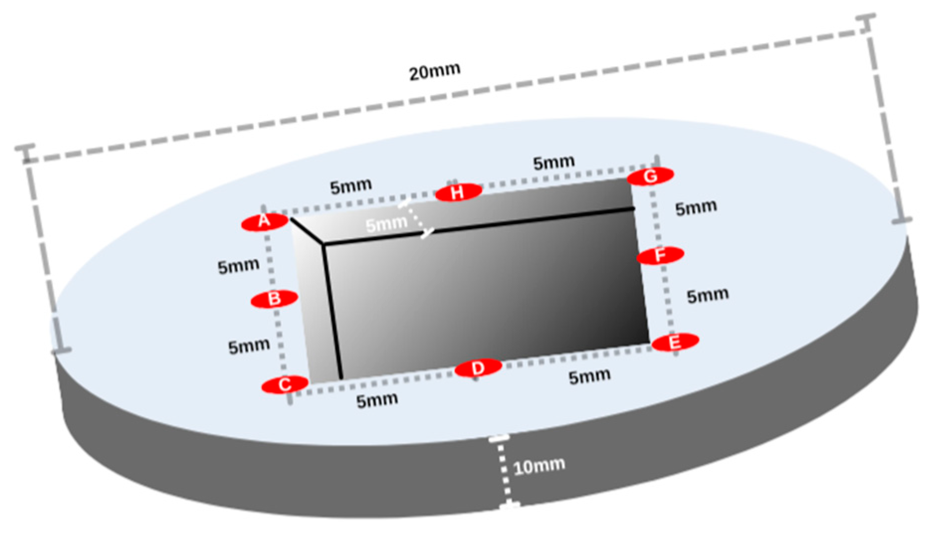
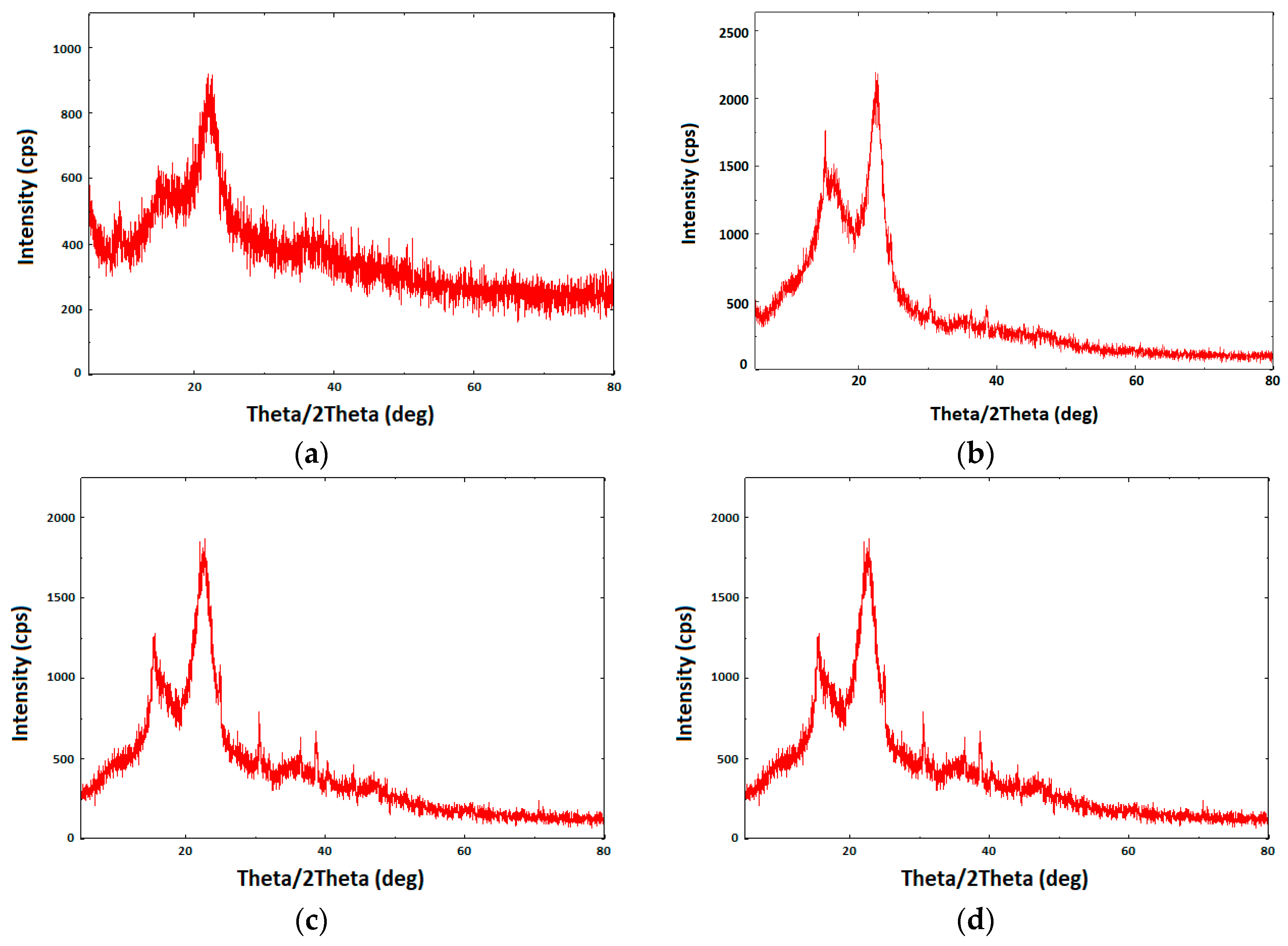
The residual stress is measured using the X-ray diffraction (XRD) technique. The workpiece is machined to a depth of 5 mm and further processed as per the standards/guidelines for XRD sample preparation (20 mm diameter and 10 mm width) and positioned in the XRD equipment, Miniflex 600, Rigaku Corporation, Tokyo, Japan. The experimental trials are conducted with CuKα radiation (λ = 1.5406 nm) at 40 kV and 15 mA in the range of 2θ = 5°–90°, with a step size of 0.02°, counting time of 1 s/step and 0.15° angle receiving slit. Measurement is conducted at eight equidistant target spots, i.e., (A–H) depicted in Figure 3 and present on the edges of the machined square slot. Further, the diffraction patterns are recorded, and data analysis is performed to determine the residual stress distribution along the surface of the workpiece. Factors such as the lattice strain and peak shift are considered to quantify the residual stress levels accurately.
Similarly, the microhardness of the samples is determined using a Vickers hardness (Vh) tester—MMT-X model from Matsuzawa Co., Ltd., Tokyo, Japan. The evaluation is carried out in accordance with the ASTM E384 standard. For the test, a diamond indenter is used to produce an indentation, with a load of 100 g and a dwell time of 10 s. The indented region on the test surface is measured using the inbuilt microscope of the Vickers hardness tester. The Vickers hardness (Vh) is calculated using Equation (2), where Fa represents the applied force (N) and Ai is the indentation area (mm2). Five measurements are recorded and the average Vickers hardness of the test samples is determined. The hardness of the AISI 316L stainless steel sample before machining is determined as 230 Hv.
V h H V = 1.854 × F a A i 2
Further, the recast layer thickness has been measured by preparing cross-sectioned samples of the workpiece. The workpiece is carefully cut as per the ASTM E3 standard to expose the EDM-machined surface, mounted on a holder, and polished to achieve a smooth and flat surface. A trinocular vertical optical microscope is used to measure the thickness of the recast layer at various locations along the cross-section. Measurements are recorded in microns and averaged to analyze the influence of the EDM parameters on the recast layer formation.
In this study, the optimization of die-sink electric discharge machining (EDM) is guided by the careful selection of the discharge current, gap voltage, pulse-on time, and pulse-off time, each set at three distinct levels (Table 5). These parameters are chosen based on an extensive literature survey, pilot experiments, and the capabilities of the EDM machine. The literature review identified these factors as crucial for influencing the material removal rate (MRR), surface roughness, and other key outputs. The pilot studies helped fine-tune the levels to ensure meaningful results while avoiding process instability. Discharge current levels of 4, 8, and 12 amperes are selected to balance the material removal and surface integrity, while gap voltage levels of 90, 110, and 130 volts are chosen to study their impact on the discharge stability and surface quality. Pulse-on times of 100, 200, and 300 microseconds are set to explore the energy delivery per discharge, and pulse-off times of 5, 10, and 15 microseconds are selected to control the cooling period between discharges, balancing the machining rates with process stability. The chosen levels align with the machine’s capabilities, ensuring reliable and optimized performance during the EDM process [51]. Though there are many optimization methods available, Taguchi’s design of experiments is chosen because of its simplicity and robustness. Since the parameters and their levels are limited, Taguchi’s design of experiments suffices for the requirements of this research. Further, Taguchi’s L27 orthogonal array is employed to design the experiment, resulting in 27 experimental runs. The material removal rate, surface roughness, residual stresses, microhardness, and recast layer thickness are measured for each experimental run. Further, ANOVA is performed to determine the significance of each factor and the interaction effects on the output parameters. And finally, the p-values are calculated to assess the significance of each factor and interaction.
A second-order polynomial model is fitted to the experimental data to establish the relationship between the input parameters and output responses. The regression coefficients are estimated to accurately quantify the impact of each factor and interaction on the output responses. The adequacy of the model is assessed using diagnostic plots and statistical tests.
Desirability functions are assigned to each output parameter based on the research objectives, i.e., maximization of the MRR and minimization of the SR, MH, RS, and RLT. The overall desirability is calculated for each combination of input parameters using the desirability functions. The combination of input parameters that maximized the overall desirability is identified as the optimal operating conditions.
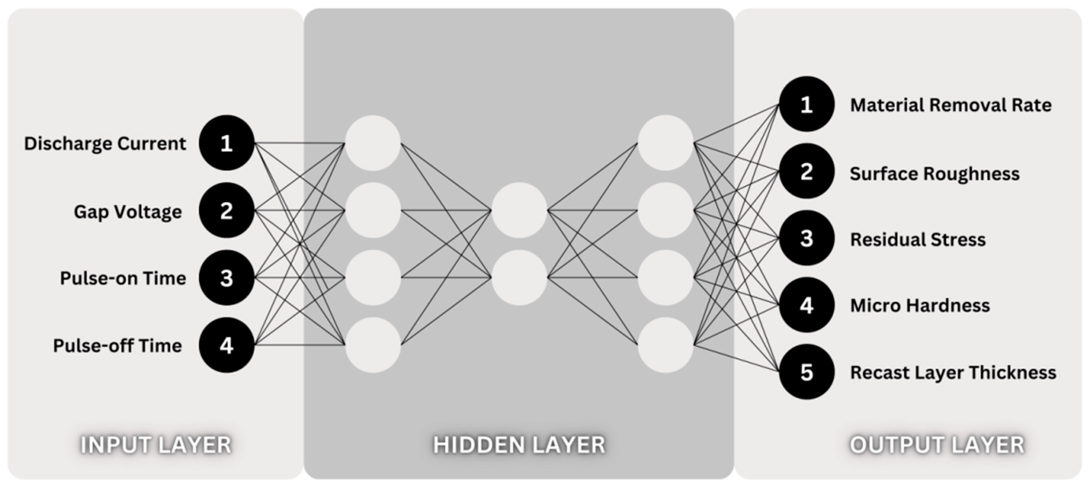
A feed-forward artificial neural network is used for predicting the output characteristics of the machining process and further steps followed during the implementation of the FFANN are given below:
  • Input and output variables are defined and the dataset is normalized.
  • FFANN architecture is defined and relevant activation functions are selected.
  • A learning algorithm is chosen and further parameters are initialized, hyperparameters are set. Finally, the data are compiled and the FFANN model is trained.
  • The dataset is split and the loss function is defined, and thus, the FFANN performance is evaluated.
  • Hyperparameters are optimized, regularization techniques are applied, and the model is fine-tuned.
  • Compared with the baselines, further FFANN interpretation is analyzed.
Figure 4 presents a schematic representation of the multi-layered feed-forward artificial neural network.

3. Results and Discussion

This section discusses about the results of the electric discharge drilling of AISI 316L SS using Ti-6Al-4V-SiCp electrodes (Table 6) and various input parameters in combination, followed by the effect of the parameters on output parameters such as the material removal rate, surface roughness, residual stress, microhardness and recast layer thickness.

3.1. Material Removal Rate

Figure 5 presents a graphical representation of the material removal rate after the electric discharge machining of AISI 316L stainless steel using the Ti-6Al-4V-SiCp electrode. Figure 6 presents the images of the electric discharge-machined holes with the machining times. After analyzing the data, it is evident that increasing the discharge current from 4 to 8, and finally to 12 amps, significantly enhances the material removal rate (MRR), which increases from 0.057 to 0.217, and eventually to 0.368 g/min. When converted into volumetric units using the density of AISI 316L stainless steel (8000 kg/m3), this corresponds to 7.13, 27.13, and 46 mm3/min, respectively. The increasing MRR can be attributed to the higher energy available with the increased current, which promotes faster material melting and vaporization. This trend is similarly reported in the works of [7], where Al-Cu-Si-TiC novel electrodes yielded an MRR ranging from 0.05 to 0.12 mm3/min. Our study shows a significant improvement of up to 283.33% in the MRR compared to these works. Additionally, the researchers in [9] observed MRR values ranging from 20 to 30 mm3/min when using Ti6Al4V electrodes. Compared to their findings, the highest MRR of 46 mm3/min observed in our work demonstrates a 53.33% improvement. AISI 316L has a relatively low thermal conductivity compared to materials like copper or titanium alloys, contributing to the formation of a localized heat-affected zone during EDM. The novel Ti-6Al-4V-SiCp electrode used in this study enhances both the thermal conductivity and electrical discharge stability, which enables faster material melting and efficient ejection of molten material. Additionally, the composite’s higher wear resistance ensures more consistent energy transfer, further improving the MRR. When examining the pulse-on times of 100, 200, and 300 µs, we observe that the MRR increases from 0.057 to 0.082, and further to 0.112 g/min (7.13, 10.25, and 14 mm3/min, respectively). This increase occurs because longer pulse-on times allow more energy to be transferred to the workpiece, resulting in greater material removal. Similar trends were observed in the works of [37] on D2 steel, where the MRR ranged between 0.05 and 0.1 mm3/min, and [38], which reported 20.5 mm3/min on D3 steel. Compared to these studies, the highest MRR achieved in our work represents a 246.95% increase. Likewise, studies on P20 steel reported MRR values of 3.2 mm3/min [39,44], while AISI 4340 steel exhibited MRR values of 9.4 to 13.2 mm3/min [42,45,46], all of which are substantially lower than the 46 mm3/min obtained in our research. The increase in the gap voltage from 90 to 130 V also positively impacts the MRR (from 0.057 to 0.112 g/min, or 7.13 to 14 mm3/min), as higher voltages promote greater energy transfer between the electrode and the workpiece. This results in more effective dielectric breakdown and increased ionization between the two, facilitating faster material erosion. Similar findings were reported by researchers in [13,33], who achieved MRR values between 0.05 and 0.1 mm3/min when machining Inconel 718 using Ti-suspended dielectric fluid. Other works on the Ti6Al4V alloy reported MRR values of 10 to 30 mm3/min [18,31], while studies on tool steel materials machined with copper electrodes yielded relatively low MRR values of 0.05 to 0.15 mm3/min [17]. Comparatively, the highest MRR of 46 mm3/min in our study represents a 53.33% improvement over these works. Conversely, increasing the pulse-off time from 5 to 15 µs results in a decrease in the MRR from 0.057 to 0.054 g/min (7.13 to 6.75 mm3/min). This decrease can be attributed to the fact that longer off-times allow the molten material to solidify before it can be effectively removed, thus slowing down the material removal process. In materials such as AISI 316L, which exhibits moderate thermal conductivity, rapid cooling results in the solidification of the molten zone, thereby reducing the MRR. Similar results have been reported in studies on tool steels [5,6,8,16,21]. At the molecular level, these variations in the MRR can be understood in terms of the energy imparted to the workpiece during the electrical discharges. Higher discharge currents and longer pulse-on times result in more intense discharges, leading to increased localized heating, melting, and vaporization of the workpiece material [19,20,32]. This results in higher material removal rates. Conversely, longer pulse-off times allow for partial cooling and solidification of the molten material, reducing the efficiency of the material removal [34,41]. Furthermore, the bonding between the electrode and the workpiece material is influenced by the temperature generated during EDM, where higher temperatures facilitate the removal of material through melting and vaporization. However, excessive heat can also lead to the formation of recast layers and heat-affected zones, which may affect the MRR and other material properties. The novel Ti-6Al-4V-SiCp composite electrode used in our study significantly outperforms other electrodes, such as Al-Cu-Si-TiC, Ti6Al4V, and copper, as evidenced by an improvement in the MRR of up to 283.33%. The enhanced performance can be attributed to the composite’s superior thermal conductivity, high hardness, and excellent wear resistance, which contribute to better energy transfer, more stable discharges, and a prolonged electrode life. These findings underscore the potential of novel composite electrodes in high-performance EDM applications, particularly for difficult-to-machine materials such as AISI 316L stainless steel. The complex interaction between the electrical discharge parameters and the material properties further highlights the importance of optimizing the EDM conditions for maximum efficiency and performance.
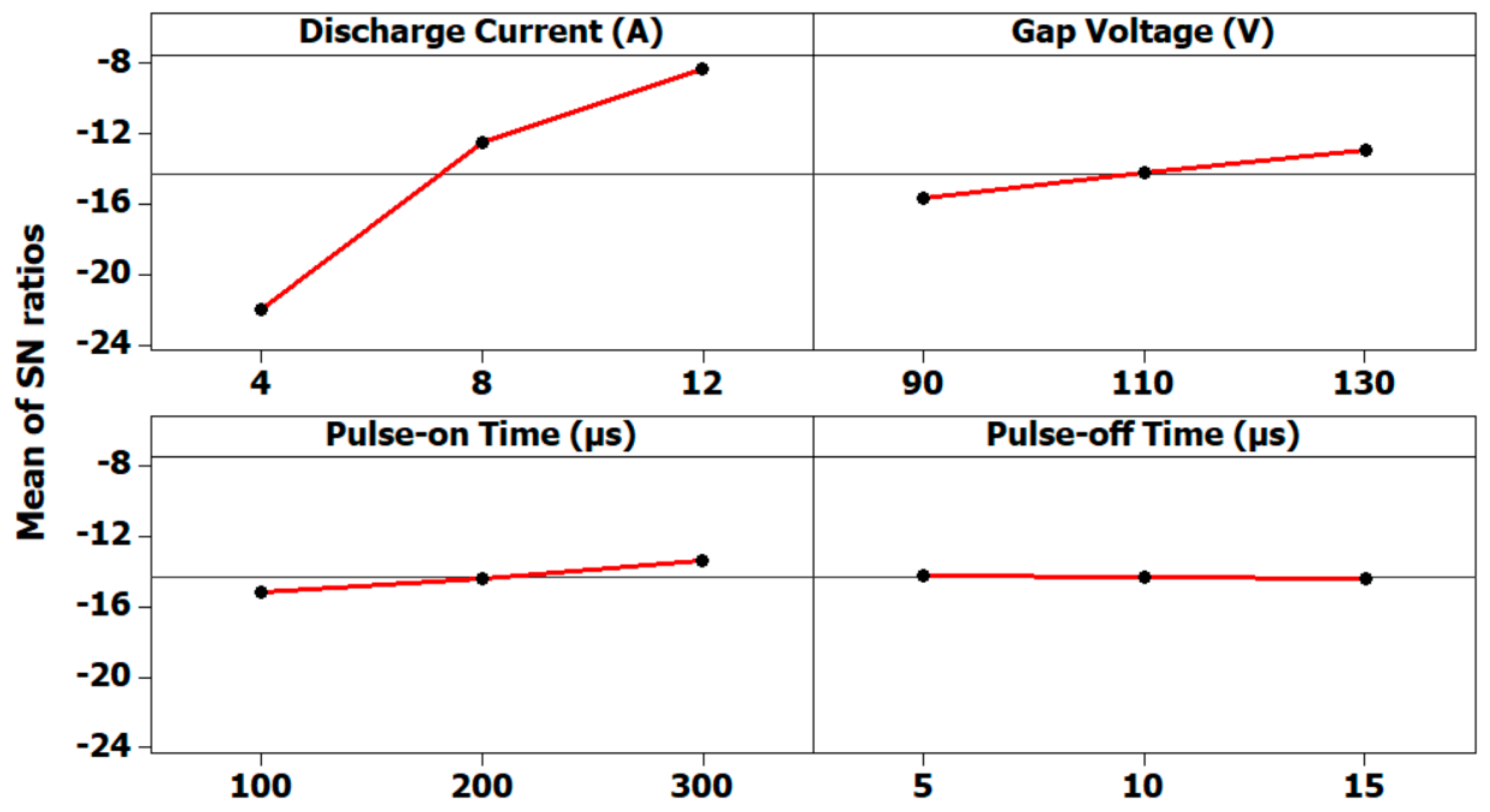
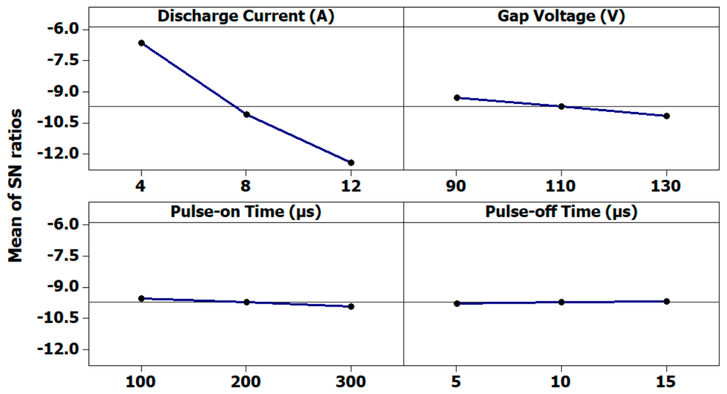
Table 7 presents the analysis of variance for the material removal rate. From the table, it can deduced that the discharge current is the most dominant parameter, which effects the material removal rate by 93.83%. Further, the gap voltage makes a significant contribution of 3.69%, followed by pulse-on time with 1.416%. The pulse-off time and the combination of parameters do not have statistical significance because of their low p%. Further, from the main effects plot (Figure 7) for the material removal rate, it can be seen that the selection of the discharge current (12 A), gap voltage (130 V), pulse-on time (300 µs), and pulse-off time (5 µs) has resulted in the optimal combination for obtaining the highest material removal rate (g/min) value during electric discharge machining of AISI 316L stainless steel using Ti-6Al-4V-SiC (15 Wt.%) composite electrodes. Further, from the figure, it can be concluded that the discharge current has the highest impact on the material removal rate, followed by the gap voltage, pulse-on time and pulse-off time.
The second-order model (Equation (3)) that has been generated using the estimated regression coefficients (Table 8) from the response surface methodology for the material removal rate can be expressed as a function of processing parameters such as the discharge current (A), gap voltage (V), pulse-on time (µs) and pulse-off time (µs), as shown in Equation (6) from the coefficients of regression estimated. The ANOVA result for the response function (material removal rate) has been provided in Table 9. In this research, a statistical analysis was conducted using a 5% level of significance, corresponding to a 95% level of confidence. The results indicate that the estimated F value from the model is greater than the critical F value from the F-distribution table (F0.05,14,16 = 5489.13), determined with 14 and 16 degrees of freedom for the numerator and denominator, respectively. The model’s ability to explain the variance in the response variable significantly exceeds that of the residual variance, confirming that the factors incorporated in the second-order response function substantially impact the response variable. Consequently, the generated second-order response function is deemed to be sufficient, capturing the essential relationships among the variables under investigation.
M a t e r i a l   R e m o v a l   R a t e   g m i n = 0.358355 + 0.053816 A + 0.003597 B 0.000132 C 0.002330 D 0.000639 A 2 0.000009 B 2 + 0.000091 D 2 0.000053 A B 0.000013 A D + 0.000003 B D
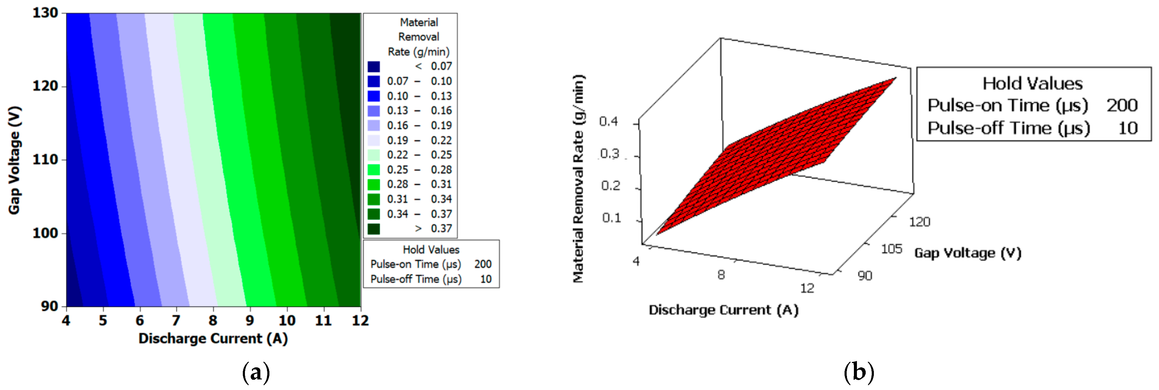
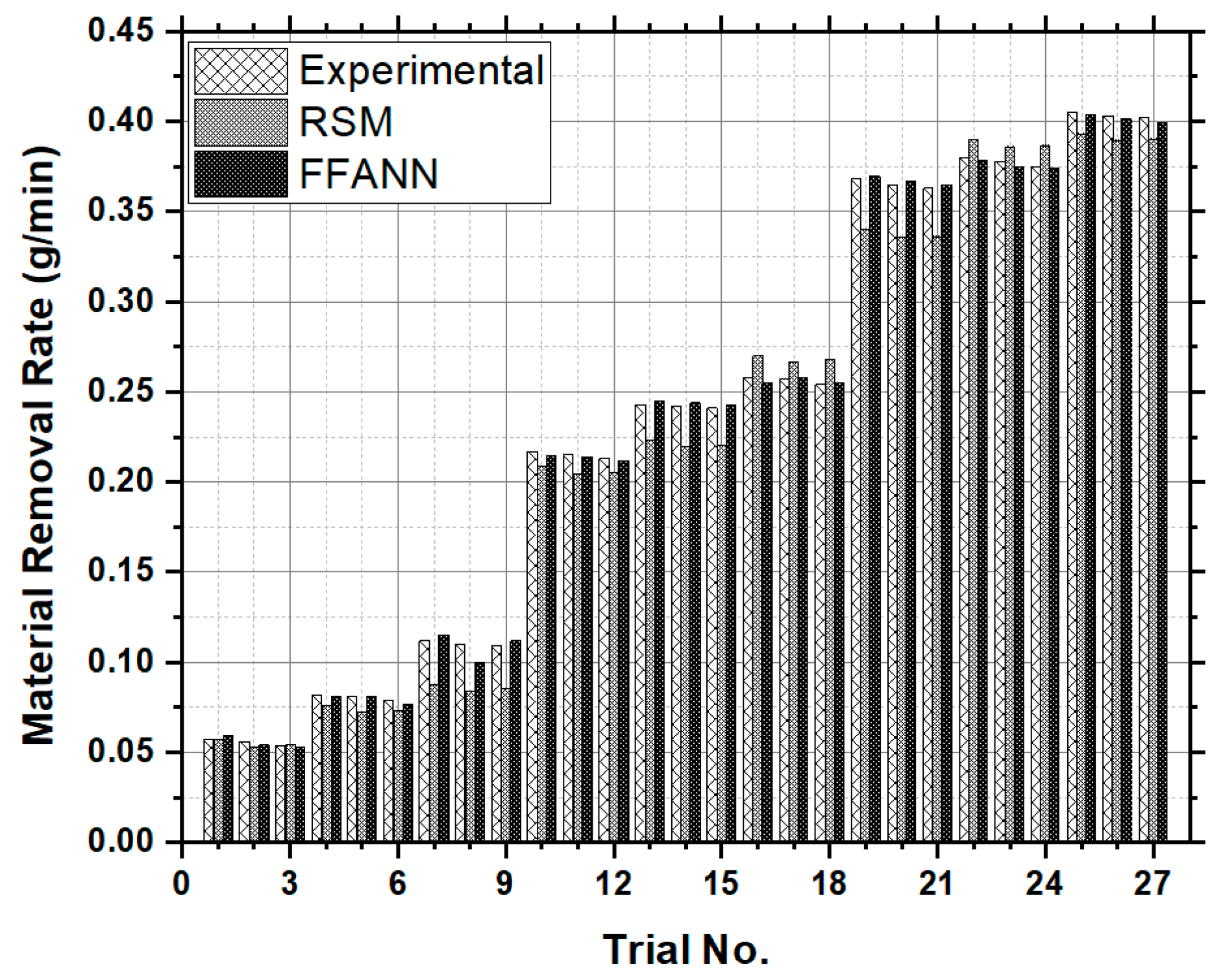
Figure 8a,b present the contour plot and surface plot for the material removal rate. The pulse-on time and pulse-off time are kept as hold values at 200 µs and 10 µs, respectively. From the figure, we can analyze that, with an 11 A discharge current and 100 V gap voltage, we can achieve the maximum material removal rate for the selected range of input parameters. Further, Figure 9 is a graphical presentation of the RSM and FFANN prediction of the material removal rate compared with the experimental results. The RSM has achieved an average error of 6.99%, with the highest deviation at 23.44% and the lowest at 0.0556% from the experimental values. Conversely, the FFANN has exhibited a lower average error of 1.48%, with its highest and lowest deviations recorded at 9.09% and 0.25%, respectively. This indicates that the FFANN outperformed the RSM in predicting the MRR, offering more accurate results across a range of conditions because of its high learning capacities, which allow for intricate dependencies between input and output parameters more effectively. However, the RSM, despite being less accurate than the FFANN, is necessary as it provides a simpler, more interpretable model, serving as a preliminary tool before applying the FFANN.

3.2. Surface Roughness

An increase in the discharge current from 4 to 8, and then to 12 Amps, correlates with a consistent decrease in the surface roughness, with values of 1.98, 3.09, and 4.09 µm, respectively (Figure 10). This inverse relationship underscores the influence of the discharge current on the surface quality, where higher currents facilitate more efficient material removal, resulting in smoother surfaces [14,15,16,20,21]. Changes in the pulse-on time significantly impact the surface roughness, with longer durations generally resulting in rougher surfaces due to the extended application of energy, which promotes more pronounced crater formation and uneven material removal. In our study, pulse-on times of 100, 200, and 300 µs yielded surface roughness values of 1.98, 2.17, and 2.36 µm, respectively. This increase in roughness with longer pulse-on times can be attributed to the greater duration of energy input, which allows for more extensive crater formation and less control over the final surface finish. Comparatively, the Al-Cu-Si-TiC composite electrode achieved a surface roughness of approximately 2.5 µm [9], which is 26.3% higher than the roughness at 200 µs and 5.9% higher than at 300 µs in our study. This increased roughness is likely due to the inherent material properties and the electrode efficiency in energy transfer. The Cu-MWCNT composite electrodes, on the other hand, resulted in a lower surface roughness of 1.5–2.0 µm [11], making our roughness values 32.0% to 57.3% higher. This disparity can be attributed to the superior energy transfer characteristics of the Cu-MWCNT composites, which likely result in finer surface finishes. Research using Al2O3 powder-suspended dielectric fluids achieved a surface finish of around 1.5 µm [22,24], which is 24.2% to 36.4% better than our maximum observed roughness of 2.36 µm. This improvement can be attributed to the enhanced cooling and flushing capabilities of Al2O3-suspended fluids, which contribute to smoother surfaces by reducing the likelihood of residual material and crater formation. In contrast, AISI 4340 steel exhibited roughness ranging from 3.5 to 3.7 µm [42,45], which is 48.5% to 86.4% higher than our highest observed roughness. The greater roughness in AISI 4340 steel can be attributed to its material properties, which might lead to more aggressive erosion and crater formation compared to the Ti-6Al-4V-SiCp electrode. High-speed steel (HSS) demonstrated roughness values of 2.0–3.0 µm [28], which is close to our roughness range, with our values being 10.6% to 17.7% lower compared to the lower end of the HSS roughness. This close comparison suggests that our electrode performs competitively in terms of the surface finish when compared to HSS under similar conditions. Finally, D3 steel machined with Al2O3 powder-suspended fluids showed a surface roughness of approximately 3.2 µm [38], which is 35.7% higher than our maximum roughness. This higher roughness in D3 steel may be due to its material characteristics and the interaction with the dielectric fluid, which may not be as effective in achieving a finer finish compared to the Ti-6Al-4V-SiCp electrodes. Overall, the Ti-6Al-4V-SiCp composite electrode demonstrates competitive performance in achieving surface finishes, particularly when compared to materials and conditions resulting in higher roughness values, such as AISI 4340 steel and D3 steel.
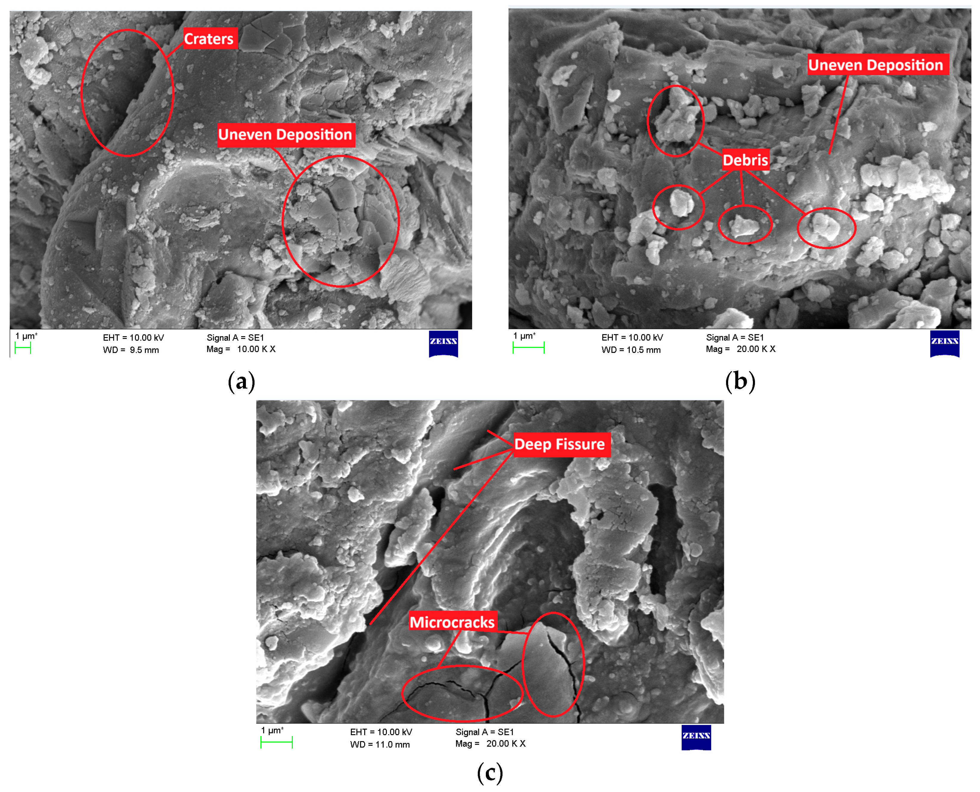
Figure 11 presents scanning electron microscopic images of sample surfaces machined under different conditions. With the low settings (Figure 11a), the surface shows minimal material removal, with localized craters and slightly uneven deposition of resolidified workpiece material, indicating insufficient energy output. However, with the medium settings (Figure 11b), increasing the levels has led to debris accumulation and pronounced uneven deposition. This suggests intensified melting and rapid resolidification, with insufficient flushing causing debris adhesion. Finally, with the highest settings (Figure 11c), the surface develops deep fissures formed because of several microcracks forming on the surface due to extreme thermal stress and rapid cooling but shows no loose deposition, suggesting efficient material ejection. At the molecular level, these changes in surface roughness can be elucidated in terms of the dynamic interactions between the electrode and the workpiece material during the EDM process. Higher discharge currents and longer pulse-on times result in more intense discharges, which can lead to smoother surfaces by facilitating more efficient material removal and minimizing surface irregularities. Conversely, longer pulse-off times may allow for partial cooling and solidification of the molten material, leading to a slight increase in the surface roughness due to the formation of microcracks on the surface. Additionally, factors such as the gap voltage and electrode material can also influence the surface roughness by affecting the energy transfer and material removal mechanisms during EDM.
Table 10 presents the analysis of variance for the surface roughness. From the table, it can deduced that the discharge current is the most dominant parameter, which effects the surface roughness by 97.13%. Further, the gap voltage makes a significant contribution of 2.243%, followed by the pulse-on time with 0.418%. The pulse-off time and the combination of parameters do not have statistical significance because of their low p%. From the main effects plot (Figure 12) for the surface roughness, it can be seen that the selection of the discharge current (4 A), gap voltage (90 V), pulse-on time (100 µs), and pulse-off time (15 µs) has resulted in the optimal combination for obtaining the lowest surface roughness (µm) value during the electric discharge machining of AISI 316L stainless steel using Ti-6Al-4V-SiC (15 Wt.%) composite electrodes. Further, from the figure, it can be concluded that the discharge current has the highest impact on the surface roughness, followed by the gap voltage, pulse-on time and pulse-off time.
The second-order model (Equation (4)) that has been generated using the estimated regression coefficients (Table 11) from the response surface methodology for the surface roughness can be expressed as a function of processing parameters such as the discharge current (A), gap voltage (V), pulse-on time (µs) and pulse-off time (µs), as shown in Equation (7) from the coefficients of regression estimated. The ANOVA result for the response function (surface roughness) has been provided in Table 12. In this research, a statistical analysis was conducted using a 5% level of significance, corresponding to a 95% level of confidence. The results indicate that the estimated F value from the model is greater than the critical F value from the F-distribution table (F0.05,14,16 = 2877.81).
S u r f a c e   R o u g h n e s s   μ m = 0.865430 + 0.361282 A + 0.02515 B 0.000966 C 0.010919 D 0.004124 A 2 0.000065 B 2 + 0.000002 C 2 + 0.000561 D 2 0.000359 A B 0.000063 A D 0.000037 B D
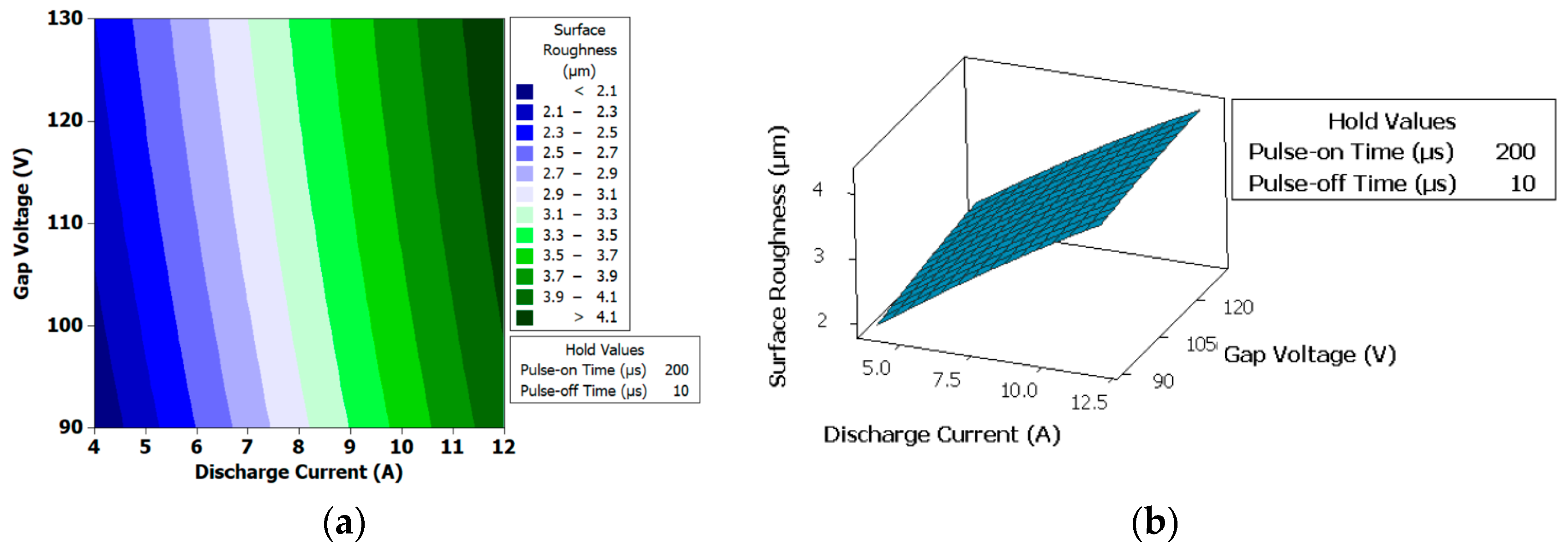
Figure 13a,b present the contour plot and surface plot for the surface roughness. The pulse-on time and pulse-off time are kept as hold values at 200 µs and 10 µs, respectively. From the figures, we can analyze that, between the 4 A and 5 A discharge current and between the 90 and 100 V gap voltage, we can achieve the lowest surface roughness for the selected range of input parameters. Further, Figure 14 is a graphical presentation of the RSM and FFANN predictions of surface roughness compared with the experimental results, with an average accuracy of 92.5% and 99.2%, respectively. In terms of the surface roughness prediction, the RSM resulted in an average error of 1.113%, with the highest deviation at 2.76% and the lowest at 0.028% from the experimental data. On the other hand, the FFANN displayed a slightly lower average error of 0.665%, with its highest and lowest deviations recorded at 1.875% and 0.231%, respectively. These findings suggest that the FFANN provides superior accuracy in predicting surface roughness compared to the RSM.

3.3. Residual Stress

From the intensity vs. theta/2theta plots (Figure 15) for the measurement of the residual stress for samples machined under various conditions, variations in the discharge current from 4 to 8, and then to 12 Amps, demonstrate a consistent increase in the residual stresses, with values of 1115.56, 2158.62, and 2808.83 MPa, respectively (Figure 16). This direct relationship underscores the influence of the discharge current on the magnitude of the residual stresses, where higher currents lead to more intense electrical discharges and subsequent material deformation, resulting in higher residual stresses. Changes in the pulse-on time exhibit a notable effect on the residual stresses, with longer pulse-on times correlating with increased residual stress values. In our study, pulse-on times of 100, 200, and 300 µs resulted in residual stresses of 1115.56, 1310.47, and 1584.91 MPa, respectively. This trend reflects the increasing energy input and consequent thermal and mechanical effects on the material, which lead to higher residual stresses. For example, the increase from 1115.56 MPa to 1584.91 MPa represents a 42.1% rise with longer pulse-on times. Similar trends have been observed in other studies, such as [15], where residual stresses exceeding 1000 MPa were recorded under comparable conditions. This correlation underscores the relationship between the energy input duration and residual stress development. In contrast, tool steel with a pulse-on time of 400 µs demonstrated lower residual stresses, ranging from 456 to 812 MPa [26]. This indicates a significant reduction of 59.1% to 71.0% in the residual stresses compared to our highest recorded value of 1584.91 MPa. The lower residual stresses in tool steel can be attributed to its different material properties and the nature of its interaction with the energy input during the machining process. The pulse-off time also affects the residual stresses, though its impact is less pronounced. Our study shows a subtle decrease in the residual stresses with increasing pulse-off times, from 1115.56 MPa at 5 µs to 1098.32 MPa at 10 µs, and further to 1063.74 MPa at 15 µs. This decrease, though modest, reflects the partial cooling and solidification of the molten material during the off-time interval, which slightly reduces the residual stress accumulation. This observation aligns with the findings of other research, where variations in the pulse-off times resulted in slight changes in the residual stress values. At the molecular level, these changes in the residual stresses can be explained in terms of the thermal and mechanical processes occurring during EDM. Higher discharge currents and longer pulse-on times result in more intense discharges and localized heating, leading to greater material deformation and subsequent residual stress formation. Conversely, longer pulse-off times allow for partial cooling and relaxation of the material, leading to a slight decrease in the residual stresses due to the reduced thermal gradients. The difference in residual stress between the machined and unmachined samples is primarily due to the intense thermal and mechanical processes during electric discharge machining (EDM). In EDM, high-energy electrical discharges cause localized heating, melting, and vaporization of the material. As the material rapidly cools, it solidifies, forming a recast layer with significant residual stresses due to the thermal gradients. In contrast, the unmachined samples, which do not undergo these extreme thermal cycles, remain in a more relaxed state, with lower residual stresses. The higher residual stresses in the machined samples are directly influenced by EDM parameters like the discharge current and pulse-on time, which increase the thermal intensity and material deformation. Table 13, Table 14 and Table 15 provide the X-ray diffraction data captured at different target points for a single sample.
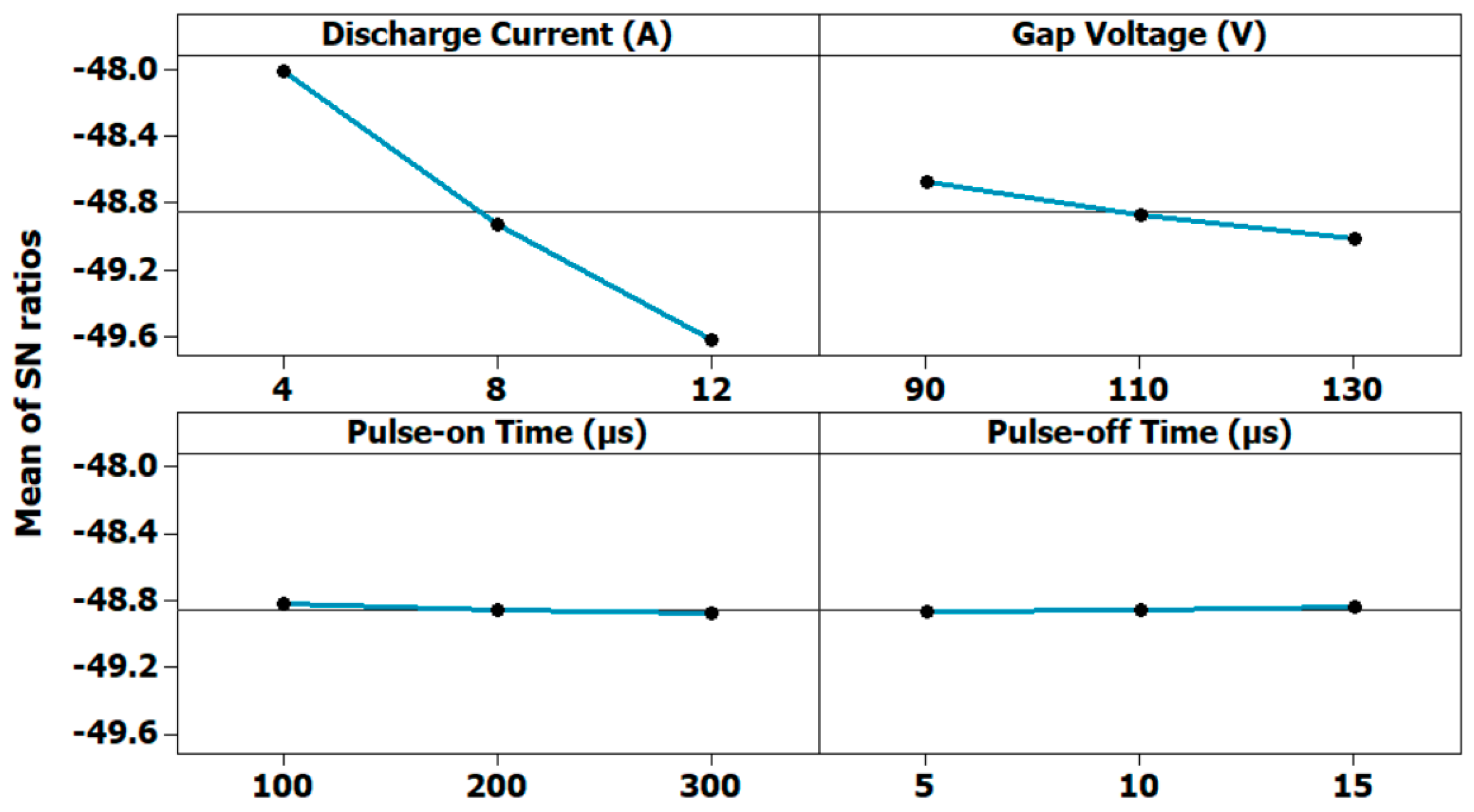
Table 16 presents the analysis of variance of signal to noise ratios for the residual stress. From the table, it can deduced that the discharge current is the most dominant parameter, which effects the material removal rate by 93.254%. Further, the gap voltage makes a significant contribution of 5.536%, followed by the pulse-on time with 0.425%. The pulse-off time and the combination of parameters do not have statistical significance because of their low p%. From the main effects plot (Figure 17) for the residual stress, it can be seen that the selection of the discharge current (4 A), gap voltage (90 V), pulse-on time (100 µs), and pulse-off time (15 µs) has resulted in the optimal combination for obtaining the lowest residual stress (MPa) value during electric discharge machining of AISI 316L stainless steel using Ti-6Al-4V-SiC (15 Wt.%) composite electrodes. Further, from the figure, it can be concluded that the discharge current has the highest impact on the surface roughness, followed by the gap voltage, pulse-on time and pulse-off time.
The second-order model (Equation (5)) that has been generated using the estimated regression coefficients (Table 17) from the response surface methodology for the residual stress can be expressed as a function of processing parameters such as the discharge current (A), gap voltage (V), pulse-on time (µs) and pulse-off time (µs), as shown in Equation (5) from the coefficients of regression estimated. The ANOVA result for the response function (residual stress) has been provided in Table 18. In the present analysis, a significance level of 5% was employed, corresponding to a confidence level of 95%. The observed F value surpasses the critical F value obtained from the F-table (F0.05,14,16 = 1930.65), implying the adequacy of the generated second-order response function. This result suggests the statistically significant fit of the model to the data, demonstrating its capacity to explain the variation in the response variable effectively within the specified confidence interval.
R e s i d u a l   S t r e s s   M P a = 1813.12 + 328.4 A + 24.44 B + 0.13 C + 7.7 D 7 A 2 0.06 B 2 0.23 D 2 0.04 A B 0.01 A D 0.09 B D
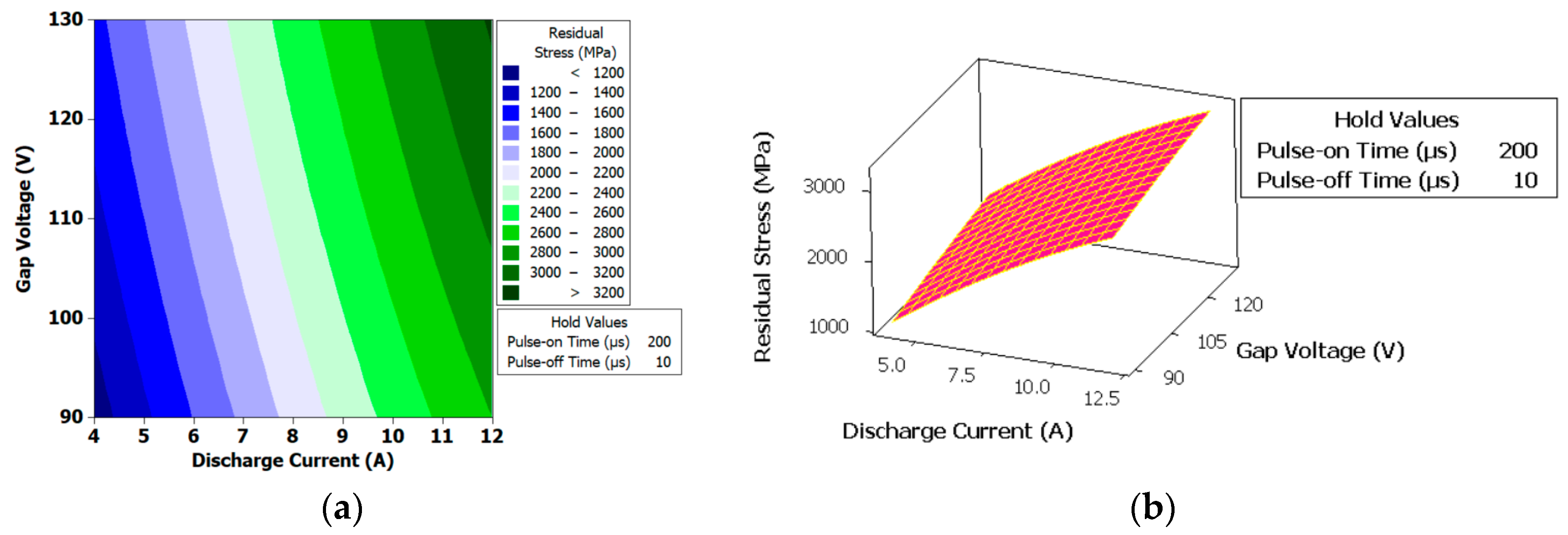
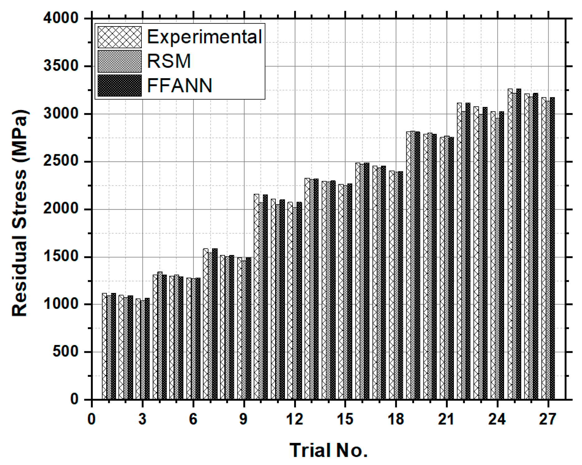
Figure 18a,b present the contour plot and surface plot for the residual stress. The pulse-on time and pulse-off time are kept as hold values at 200 µs and 100 µs, respectively. From the figure, we can analyze that, with an 4 A discharge current and 90 V gap voltage, we can achieve the least residual stress for the selected range of input parameters. Further, Figure 19 is a graphical presentation of the RSM and FFANN prediction of residual stress compared with the experimental results, with an average accuracy of 93.7% and 99.2%, respectively. For the residual stress estimation, the RSM yielded an average error of 1.53%, with the highest deviation at 4.164% and the lowest at 0.349% from the experimental observations. Conversely, the FFANN exhibited a significantly lower average error of 0.159%, with its highest and lowest deviations recorded at 0.307% and 0.079%, respectively. These results underscore the FFANN’s superiority over the RSM in predicting residual stress, offering more precise outcomes across various scenarios.

3.4. Microhardness

From the graphical representation of the microhardness (Figure 20), it is evident that variations in the discharge current have a substantial impact on the microhardness. Specifically, increasing the discharge current from 4 to 8, and then to 12 Amps, results in corresponding increases in the microhardness, with values of 245.9, 274.1, and 298.3 Hv, respectively, compared to a base value of 230 Hv. This trend highlights the direct relationship between the discharge current and the microhardness. Higher discharge currents produce more intense electrical discharges, which enhance the material hardening through the increased thermal effects and phase transformations, leading to higher microhardness values. Similarly, changes in the pulse-on time influence the microhardness, with longer pulse-on times correlating with higher microhardness values. For instance, pulse-on times of 100, 200, and 300 µs result in microhardness values of 245.9, 253.1, and 257.6 Hv, respectively. This increase reflects the extended energy input during each discharge, which contributes to the greater material deformation and subsequent microstructural alterations, which enhance the hardness. This effect is consistent with the findings of other research, where similar increases in the pulse-on time lead to higher hardness values, though the variations can depend on specific conditions and materials. In comparison, research on P20 steel using Cu electrodes has shown microhardness levels of 310 Hv compared to 300 Hv, and another study on P20 steel reported a significant increase to 400 Hv under similar conditions [39,40]. These values are lower than those observed in our study, highlighting the superior hardening effect of the novel Ti-6Al-4V-SiCp electrodes used. Conversely, variations in the pulse-off time have a less pronounced effect on the microhardness. Our study reveals subtle changes in the microhardness from 245.9 Hv at 5 µs to 245.4 Hv at 10 µs, and then to 244.8 Hv at 15 µs. This minor fluctuation indicates that while the pulse-off time impacts the cooling and solidification process, its effect on the microhardness is less significant compared to the discharge current and pulse-on time. For example, research on AISI 4340 steel using copper electrodes has reported a notable increase in hardness from 380 Hv to 450 Hv [42]. In contrast, a study on H13 steel demonstrated a substantial decrease in hardness from 950 Hv to 480 Hv using Cu-W electrodes, illustrating how the material composition and electrode type can greatly influence the hardness outcomes under different EDM conditions. At the molecular level, these changes in microhardness can be explained in terms of the thermal and mechanical processes occurring during EDM. Higher discharge currents and longer pulse-on times result in more intense discharges and localized heating, leading to increased material hardening through phase transformations and grain refinement. Conversely, longer pulse-off times may allow for partial cooling and relaxation of the material, resulting in minimal changes in the microhardness. Additionally, factors such as the gap voltage and electrode material can indirectly influence the microhardness by affecting the material removal mechanisms and subsequent microstructural changes during EDM.
Table 19 presents the analysis of variance for the microhardness. From the table, it can deduced that the discharge current is the most dominant parameter, which effects the material removal rate by 95.39%. Further, the gap voltage makes a significant contribution of 4.401%, followed by the pulse-on time with 0.136%. The pulse-off time and the combination of parameters do not have statistical significance because of their low p%. From the main effects plot (Figure 21) for the microhardness, it can be seen that the selection of the discharge current (4 A), gap voltage (90 V), pulse-on time (100 µs), and pulse-off time (15µs) has resulted in the optimal combination for obtaining the highest microhardness (Hv) value during electric discharge machining of AISI 316L stainless steel using Ti-6Al-4V-SiC (15 Wt.%) composite electrodes. Further, from the figure, it can be concluded that the discharge current has the highest impact on the microhardness followed, by the gap voltage, pulse-on time and pulse-off time.
The second-order model (Equation (6)) that has been generated using the estimated regression coefficients (Table 20) from the response surface methodology for the microhardness can be expressed as a function of processing parameters such as the discharge current (A), gap voltage (V), pulse-on time (µs) and pulse-off time (µs), as shown in Equation (6) from the coefficients of regression estimated. The ANOVA result for the response function (microhardness) has been provided in Table 21. The analysis is conducted at a 5% level of significance, corresponding to a 95% level of confidence. The estimated F value exceeds the F-table value (F0.05,14,16 = 803.96), indicating the adequacy of the generated second-order response function, suggesting the statistically significant fit of the model to the data.
M i c r o h a r d n e s s   H v = 129.329 + 9.627 A + 1.309 B 0.019 C + 0.424 D 0.219 A 2 0.004 B 2 0.010 D 2 0.001 A B + 0.001 A C + 0.018 A D 0.003 B D 0.001 C D
Figure 22a,b present the contour plot and surface plot for the microhardness. The pulse-on time and pulse-off time are kept as hold values at 200 µs and 100 µs, respectively. From the figure, we can analyze that, with a 4 A discharge current and between 90 and 110 V gap voltage, we can achieve the least microhardness for the selected range of input parameters. Further, Figure 23 is a graphical presentation of the RSM and FFANN prediction of the microhardness compared with the experimental results, with an average accuracy of 92.8% and 99.3%, respectively. Regarding the microhardness prediction, the RSM showed an average error of 1.172%, with the highest deviation at 2.934% and the lowest at 0.087% from the experimental data. In contrast, the FFANN demonstrated a substantially lower average error of 0.165%, with its highest and lowest deviations recorded at 0.67% and 0%, respectively. This indicates that the FFANN excels in predicting the microhardness, providing more accurate estimations compared to the RSM.

3.5. Recast Layer Thickness

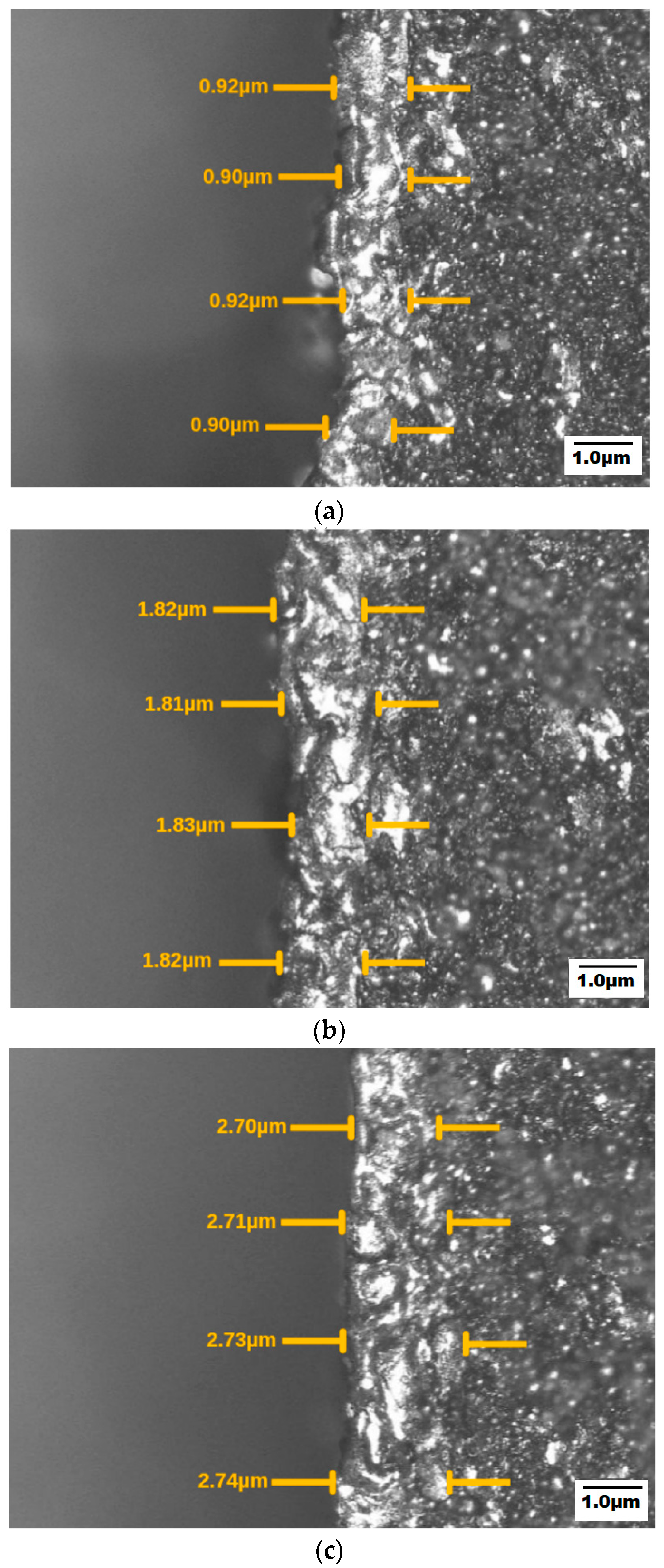
Figure 24 presents a graphical representation of the recast layer thickness after electric discharge machining of AISI 316L stainless steel using the Ti-6Al-4V-SiCp electrode. Figure 25 presents the trinocular vertical microscopic images of the recast layer formed after electric discharge machining. Variations in the discharge current from 4 to 8, and then to 12 Amps, demonstrate a marked increase in the recast layer thickness, with values of 0.53, 1.42, and 2.32 µm, respectively. This trend illustrates the significant influence of the discharge current on the recast layer formation. As the discharge current increases, the intensity of the electrical discharges and thermal energy rises, leading to a thicker recast layer. Specifically, increasing the discharge current from 4 to 8 Amps results in a 167.92% increase in the recast layer thickness (from 0.53 to 1.42 µm), and a further increase to 12 Amps results in an additional 62.68% increase (from 1.42 to 2.32 µm). This substantial rise underscores the impact of higher currents on the material redeposition and recast layer thickness. Similarly, the pulse-on time affects the recast layer thickness, with longer pulse-on times leading to increased thickness. For pulse-on times of 100, 200, and 300 µs, the recast layer thickness increases from 0.53 to 0.72 µm and then to 0.91 µm. This represents a 35.85% increase when extending from 100 to 200 µs and an additional 26.39% increase from 200 to 300 µs. Longer pulse-on times allow more energy to be transferred to the workpiece per discharge, contributing to the thicker recast layers as the thermal impact and material redeposition are enhanced. Conversely, the pulse-off time has a less pronounced effect on the recast layer thickness. For pulse-off times of 5, 10, and 15 µs, the recast layer thickness slightly decreases from 0.53 to 0.51 µm and then to 0.47 µm. This results in a 3.77% decrease from 5 to 10 µs and a further 7.84% decrease from 10 to 15 µs. The reduction is attributed to the partial cooling and solidification of molten material during the pulse-off period, which minimizes the redeposition. Comparative studies highlight the context of our findings. Research on AISI 316L stainless steel shows similar trends, with the reported recast layer thickness aligning closely with our results [27]. In contrast, a study on D3 steel using Al2O3-suspended dielectric fluids reports a significantly higher recast layer thickness of approximately 8 µm [38]. This represents a 2440% increase compared to our maximum of 2.32 µm. Additionally, a wire EDM study on 316L stainless steel has documented recast layer deposition in the range of 3.5 to 4.3 µm, which is approximately 50.43% to 85.71% higher than our observed maximum of 2.32 µm. These comparisons indicate that while our study’s recast layer thickness is lower than those reported for the D3 steel and wire EDM processes, the observed trends and increases with varying parameters are consistent with the broader understanding of recast layer formation.
At the molecular level, these changes in the recast layer thickness can be elucidated in terms of the thermal and mechanical processes occurring during EDM. Higher discharge currents and longer pulse-on times result in more intense discharges and localized heating, leading to increased material redeposition and subsequent recast layer formation. Conversely, longer pulse-off times may allow for partial cooling and solidification of the molten material, resulting in slightly thinner recast layers due to the reduced thermal gradients. Additionally, factors such as the gap voltage and electrode material can indirectly influence the recast layer thickness by affecting the material removal mechanisms and subsequent material redeposition during EDM.
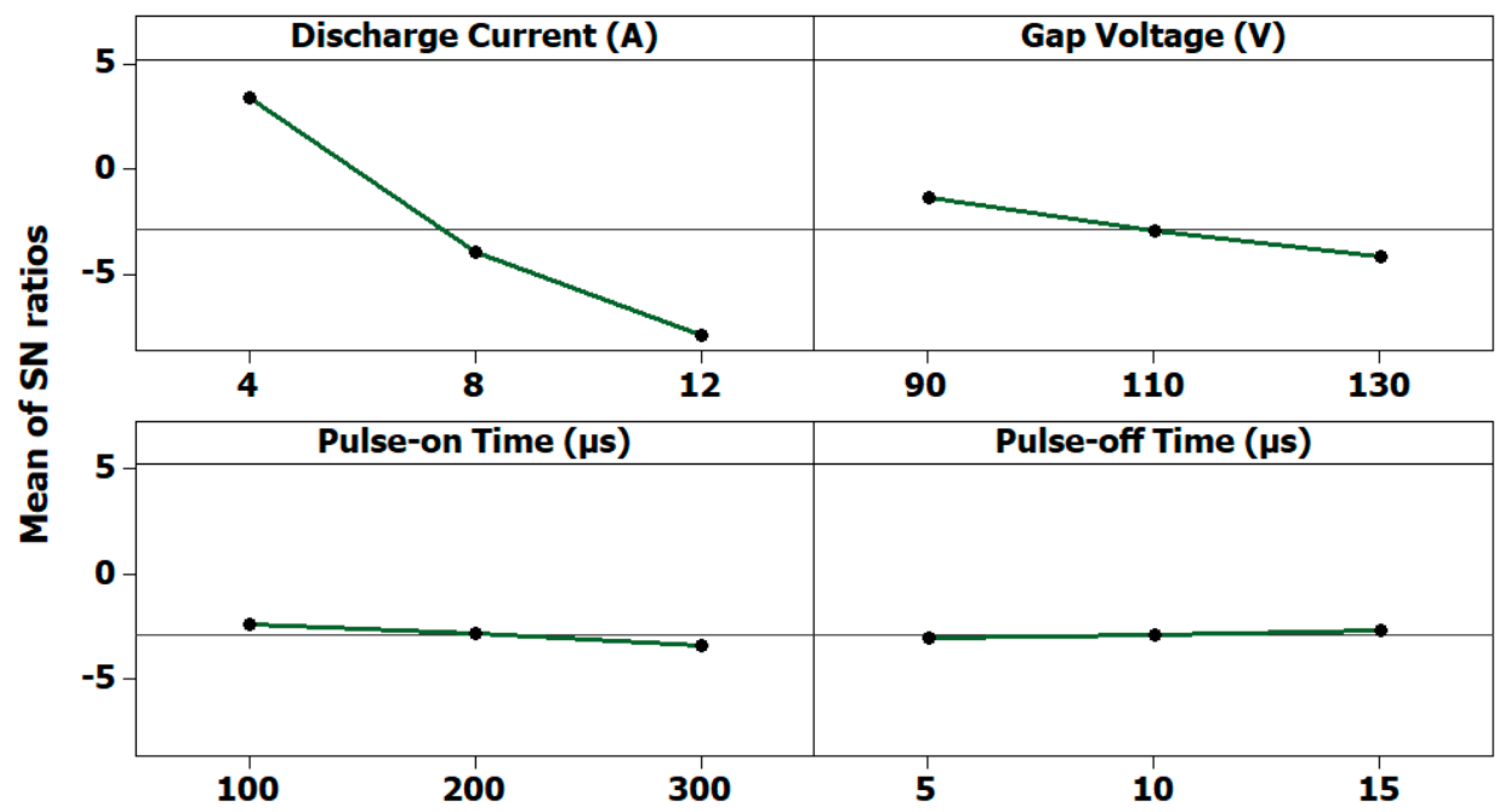
Table 22 presents the analysis of variance for the recast layer thickness. From the table, it can deduced that the discharge current is the most dominant parameter, which effects the material removal rate by 92.51%. Further, the gap voltage makes a significant contribution of 5.721%, followed by the pulse-on time with 0.701%. The pulse-off time and the combination of parameters do not have statistical significance because of their low p%. From the main effects plot (Figure 26) for the recast layer thickness, it can be seen that the selection of the discharge current (4 A), gap voltage (90 V), pulse-on time (100 µs), and pulse-off time (15 µs) has resulted in the optimal combination for obtaining the lowest recast layer thickness (µm) value during electric discharge machining of AISI 316L stainless steel using Ti-6Al-4V-SiC (15 Wt.%) composite electrodes. Further, from the figure, it can be concluded that the discharge current has the highest impact on the recast layer thickness, followed by the gap voltage, pulse-on time and pulse-off time.
The second-order model (Equation (7)) that has been generated using the estimated regression coefficients (Table 23) from the response surface methodology for the recast layer thickness can be expressed as a function of processing parameters such as the discharge current (A), gap voltage (V), pulse-on time (µs) and pulse-off time (µs), as shown in Equation (7) from the coefficients of regression estimated. The ANOVA result for the response function (recast layer thickness) has been provided in Table 24. The analysis was conducted with a 5% level of significance, corresponding to a 95% level of confidence. The estimated F value surpasses the F-table value (F0.05,14,16 = 25,557.34), suggesting the adequacy of the generated second-order response function.
R e c a s t   L a y e r   T h i c k n e s s   μ m = 0.952350 + 0.210431 A + 0.004631 B + 0.000245 C + 0.001476 D + 0.000538 A 2 + 0.000021 B 2 0.000001 C 2 0.000456 D 2 + 0.000047 A B + 0.000188 A D + 0.000012 B D
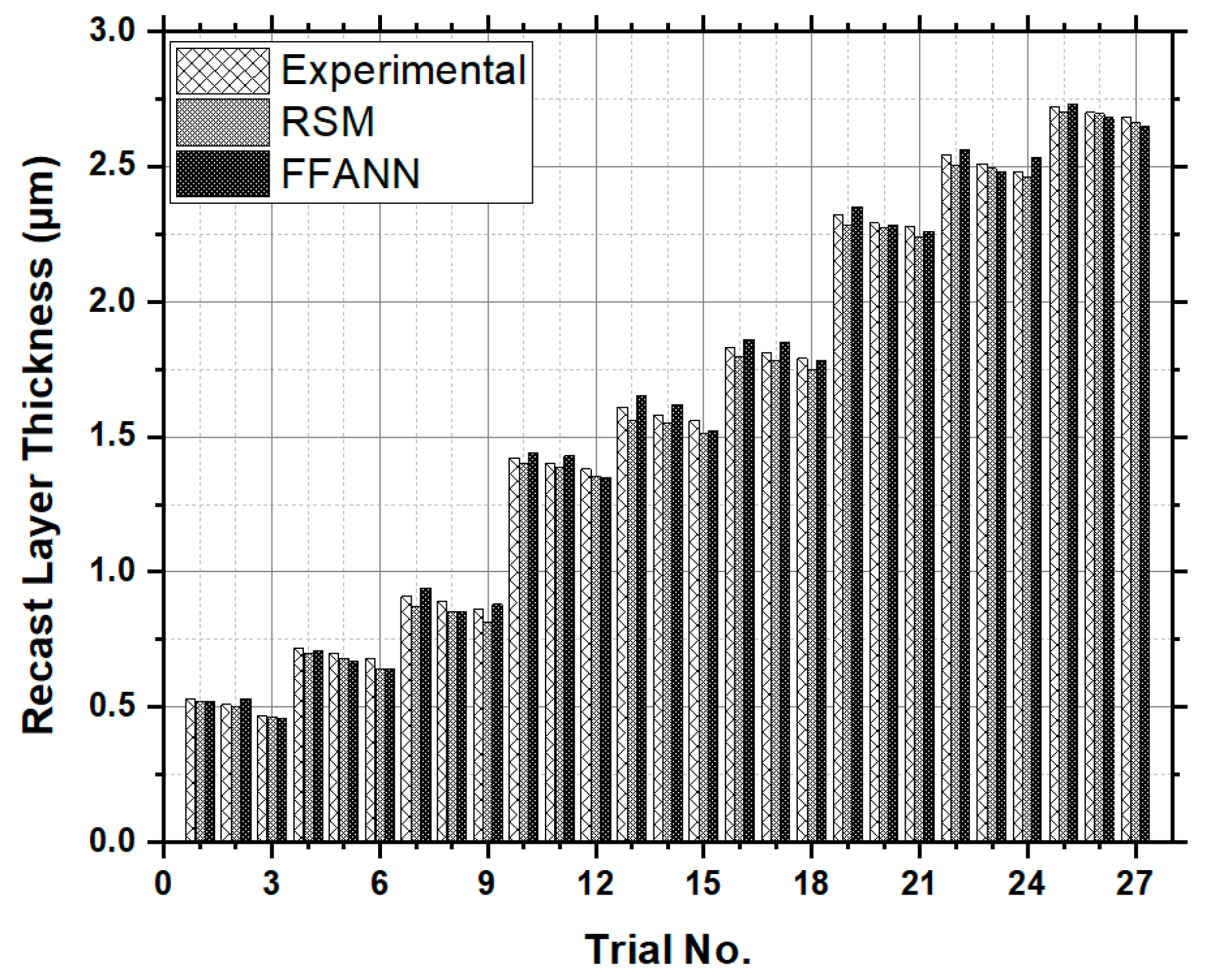
Figure 27a,b present the contour plot and surface plot for the recast layer thickness. The pulse-on time and pulse-off time are kept as hold values at 200 µs and 100 µs, respectively. From the figures, we can analyze that, with a 4 A discharge current and between 90 and 110 V gap voltage, we can achieve the least recast layer thickness for the selected range of input parameters. Further, Figure 28 is a graphical presentation of the RSM and FFANN prediction of the recast layer thickness compared with the experimental results, with an average accuracy of 94.2% and 98.4%, respectively. In predicting the recast layer thickness, the RSM resulted in an average error of 1.975%, with the highest deviation at 5.62% and the lowest at 0.116% from the experimental measurements. Conversely, the FFANN exhibited a slightly higher average error of 2.08%, with its highest and lowest deviations recorded at 5.88% and 0.559%, respectively. These findings suggest that while the FFANN and RSM perform comparably in predicting the recast layer thickness, the RSM may offer slightly more consistent results across different conditions.
In comparing the response surface methodology (RSM) and feed-forward artificial neural networks (FFANNs) for predicting the material removal rate (MRR), each method has distinct advantages and disadvantages. The RSM is advantageous due to its simplicity and interpretability, making it a useful preliminary tool for understanding how input parameters influence outcomes through clear mathematical expressions. However, its assumption of linear or quadratic relationships limits its ability to capture complex, non-linear dependencies, which can lead to significant prediction errors. Conversely, the FFANN excels in modeling these intricate, non-linear relationships due to its high learning capacity, resulting in more accurate predictions across varied conditions. The trade-off, however, is its complexity and “black-box” nature, which make it less interpretable and more reliant on large datasets for effective training. A key limitation in this study was the small dataset, stemming from the limited number of experiments, which can constrain the performance of both the RSM and FFANN but poses a greater challenge for the FFANN, which typically requires more data for optimal accuracy. Future researchers should consider these factors when choosing between the RSM and the FFANN, weighing the need for model interpretability and simplicity against the desire for higher accuracy and the ability to model complex interactions, while also taking into account the availability of sufficient data to support the chosen method.
The practical implications of comparing the RSM and FFANN in predicting the material removal rate (MRR) for EDM processes are significant. While the RSM offers simplicity and interpretability, its higher error rate suggests limitations in accurately capturing complex, non-linear relationships, which can lead to suboptimal machining outcomes and increased costs in precision-critical industries. In contrast, the FFANN’s lower error rate demonstrates its superior capability in providing accurate predictions, essential for optimizing EDM processes. However, the FFANN’s effectiveness depends on having a sufficiently large dataset, highlighting the need for extensive data collection. This study suggests that while the RSM can serve as a useful initial tool, the FFANN is better suited for achieving high accuracy in machining processes, with future research focusing on hybrid models and larger datasets to enhance both the accuracy and interpretability.

3.6. Desirability Function Analysis

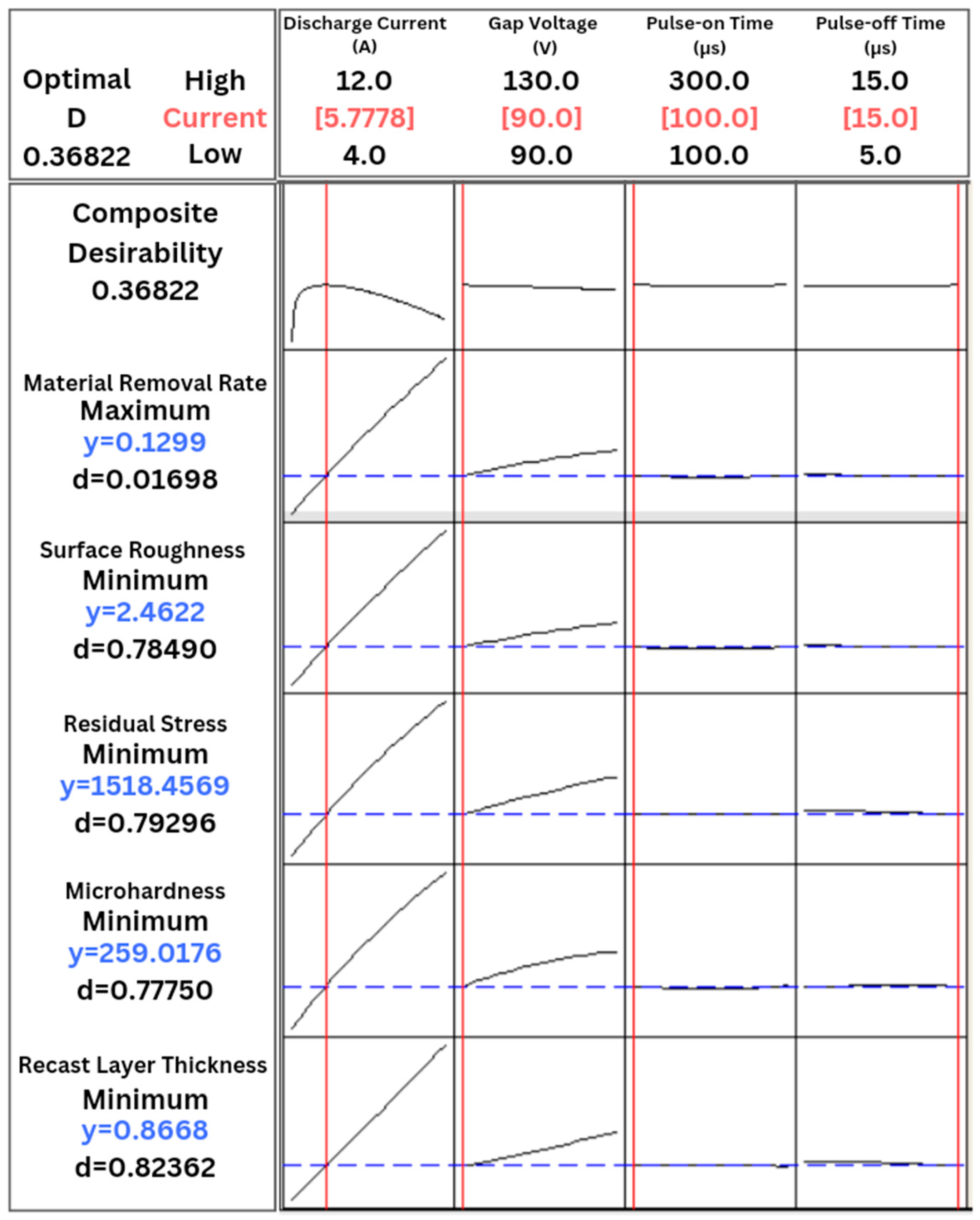
In the desirability function analysis (Figure 29), the optimal desirability (D) value obtained is 0.36822, indicating the desired combination of parameters for achieving the desired outcomes. The parameters and their respective levels are as follows: discharge current (A) set at 5.7778 A, gap voltage (V) at 90.0 V, pulse-on time at 100.0 microseconds, and pulse-off time at 15.0 microseconds. These settings collectively yield the composite desirability of 0.36822, suggesting an optimal configuration for the process under study. Moreover, the performance of the optimized parameters is assessed based on various response variables. The material removal rate is maximized, achieving a value of 0.1299, with a desirability score of 0.01698. The surface roughness is minimized to 2.4622, with a desirability score of 0.78490, while the residual stress is minimized to 1518.4569, with a desirability score of 0.79296. Additionally, the microhardness is minimized to 259.0176, with a desirability score of 0.7775, and the recast layer thickness is minimized to 0.8668, with a desirability score of 0.82362. These findings provide insights into the optimal parameter settings required to achieve the desired outcomes in terms of the material removal rate, surface roughness, residual stress, microhardness, and recast layer thickness, thereby facilitating the optimization of the process for enhanced performance and quality.

4. Conclusions

Based on the experimental results, the following conclusions are drawn. This study underscores the significant influence of various process parameters on key outcomes in the electric discharge machining (EDM) of AISI 316L stainless steel using a Ti-6Al-4V-SiCp composite electrode. The findings reveal that increasing the discharge current and pulse-on time results in higher material removal rates (MRRs), as more energy is transferred to the workpiece, while longer pulse-off times slightly reduce the MRR due to partial cooling. These parameters also impact the surface roughness, with higher currents and extended pulse-on times producing smoother surfaces, though the pulse-off time has a minimal effect. Additionally, higher discharge currents and longer pulse-on times lead to increased residual stresses, which could affect the long-term performance of machined components. In terms of the microhardness, higher currents and longer pulse-on times enhance the material hardness, which may be advantageous depending on the application. This study also shows that these parameters cause thicker recast layers due to the intensified material redeposition and prolonged thermal exposure, with the pulse-off times having only a minor effect.
Moreover, the response surface methodology (RSM) model applied in this research has proven sufficient for predicting the outcomes based on the input parameters, providing a robust framework for understanding the complex relationships involved. However, to capture the non-linear interactions more effectively, a feed-forward artificial neural network (FFANN) was employed, demonstrating its superiority in predicting the output parameters with higher accuracy than traditional models. This dual approach ensures a comprehensive optimization of the EDM process, offering valuable insights for achieving the best possible machining performance.
However, this study does have some limitations, particularly related to the range of levels and the specific process parameters considered. The research was constrained by a limited number of levels for the discharge current, pulse-on time, pulse-off time, and gap voltage, which may restrict the generalizability of the findings. Additionally, parameters related to the dielectric fluid, such as its type, temperature, and flow rate, were not explored in this study, potentially overlooking their significant impact on the EDM performance. Future research should aim to investigate a wider range of input levels and incorporate parameters related to the dielectric fluid to provide a more comprehensive understanding of the EDM process. Moreover, expanding the study to include different work materials and electrodes would further enhance the applicability of the findings, allowing for broader optimization strategies in various industrial contexts.

Author Contributions

Conceptualization, A.H. and R.S.; methodology, A.H., R.S., S.S. and U.K.S.S.; software, A.H. and R.N.; validation, A.H., R.S. and S.S.; formal analysis, A.H.; investigation, A.H.; resources, A.H.; data curation, A.H.; writing—original draft preparation, A.H.; writing—review and editing, A.H.; visualization, A.H.; supervision, R.S. and R.N.; project administration, R.S.; funding acquisition, R.N, S.S. and U.K.S.S. All authors have read and agreed to the published version of the manuscript.

Funding

This research received no external funding.

Data Availability Statement

All data are embedded within the article.

Conflicts of Interest

The authors declare no conflicts of interest.

Abbreviations

DoEDesign of Experiments
EDMElectric Discharge Machining
RSMResponse Surface Methodology
DFADesirability Function Analysis
ANOVAAnalysis of Variance
FFANNFeed-Forward Artificial Neural Network
AISIAmerican Iron and Steel Institute
Adj SSAdjusted Sum of Squares
Adj MSAdjusted Mean of Squares
MRRMaterial Removal Rate
EWRElectrode Wear Rate
TWRTool Wear Rate
SRSurface Roughness
RLTRecast Layer Thickness
MHMicrohardness
RSResidual Stress
DFDegrees of Freedom

References

  1. Banu, A.; Ali, M.Y. Electrical discharge machining (EDM): A review. Int. J. Eng. Mater. Manuf. 2016, 1, 3–10. [Google Scholar] [CrossRef]
  2. Liao, Y.S.; Chen, S.T.; Lin, C.S. Development of a high precision tabletop versatile CNC wire-EDM for making intricate micro parts. J. Micromech. Microeng. 2005, 15, 245–253. [Google Scholar] [CrossRef]
  3. Abbas, M.N.; Solomon, D.G.; Fuad Bahari, M. A review on current research trends in electrical discharge machining (EDM). Int. J. Mach. Tools Manuf. 2007, 47, 1214–1228. [Google Scholar] [CrossRef]
  4. Jagtap, M.; Karande, P. The m-polar fuzzy ELECTREI integrated AHP approach for selection of non-traditional machining processes. Cogent Eng. 2023, 10, 2181737. [Google Scholar] [CrossRef]
  5. Mao, X.; Almeida, S.; Mo, J.; Ding, S. The state of the art of electrical discharge drilling: A review. Int. J. Adv. Manuf. Technol. 2022, 121, 2947–2969. [Google Scholar] [CrossRef]
  6. Patnaik, P.K.; Mishra, S.K.; Swain, P.T.R.; Purohit, A.; Parija, S.K.; Panda, S.S. Multi-objective optimization and experimental analysis of electro-discharge machining parameters via Gray-Taguchi, TOPSIS-Taguchi and PSI-Taguchi methods. Mater. Today Proc. 2022, 62, 6189–6198. [Google Scholar] [CrossRef]
  7. El-Taweel, T.A. Multi-response Optimization of EDM with Al-Cu-Si-TiC P/M Composite Electrode. Int. J. Adv. Manuf. Technol. 2009, 44, 100–113. [Google Scholar] [CrossRef]
  8. Sohani, M.S.; Gaitonde, V.N.; Siddeswarappa, B.; Deshpande, A.S. Investigations into the Effect of Tool Shapes with Size Factor consideration in Sink Electrical Discharge Machining EDM Process. Int. J. Adv. Manuf. Technol. 2009, 45, 1131–1145. [Google Scholar] [CrossRef]
  9. Asif Iqbal, A.K.M.; Khan, A.A. Modeling and Analysis of MRR, EWR and Surface Roughness in EDM Milling through Response Surface Methodology. Am. J. Eng. Appl. Sci. 2010, 3, 611–619. [Google Scholar]
  10. Yoo, H.K.; Kwon, W.T.; Kang, S. Development of a new electrode for micro-electrical discharge machining (EDM) using Ti(C,N)-based cermet. Int. J. Precion Eng. Manuf. 2014, 15, 609–616. [Google Scholar] [CrossRef]
  11. Mandal, P.; Mondal, S.C. Multi-objective optimization of Cu-MWCNT composite electrode in electro discharge machining using MOPSO-TOPSIS. Measurement 2021, 169, 108347. [Google Scholar] [CrossRef]
  12. Kumari, S.; Sonia, P.; Singh, B.; Abhishek, K.; Saxena, K.K. Optimization of surface roughness in EDM of pure magnesium (Mg) using TLBO. Mater. Today Proc. 2020, 26, 2458–2461. [Google Scholar] [CrossRef]
  13. Bhowmick, S.; Mondal, R.; Sarkar, S.; Biswas, N.; De, J.; Majumadar, G. Parametric optimization and prediction of MRR and surface roughness of titanium mixed EDM for inconel 718 using RSM and fuzzy logic. CIRP J. Manuf. Sci. Technol. 2023, 40, 10–28. [Google Scholar] [CrossRef]
  14. Reddy, B.S.; Rao, A.K.; Janardhana, G.R. Multi-objective optimization of surface roughness, recast layer thickness and surface crack density in WEDM of Al2124/SiCp using desirability approach. Mater. Today Proc. 2021, 39, 1320–1326. [Google Scholar] [CrossRef]
  15. Rajhi, W.; Alatawi, I.; Subhani, T.; Ayadi, B.; Al-Ghamdi, A.; Khaliq, A. A contribution to numerical prediction of surface damage and residual stresses on die-sinking EDM of Ti6Al4V. J. Manuf. Process. 2021, 68, 1458–1484. [Google Scholar] [CrossRef]
  16. Shastri, R.K.; Mohanty, C.P. Sustainable Electrical Discharge Machining of Nimonic C263 Superalloy. Arab. J. Sci. Eng. 2021, 46, 7273–7293. [Google Scholar] [CrossRef]
  17. Straka, L.; Hašová, S. Optimization of material removal rate and tool wear rate of Cu electrode in die-sinking EDM of tool steel. Int. J. Adv. Manuf. Technol. 2018, 97, 2647–2654. [Google Scholar] [CrossRef]
  18. Rahman, M.M.; Khan, M.A.R.; Kadirgama, K.; Noor, M.M.; Bakar, R.A. Modeling of material removal on machining of Ti-6Al-4V through EDM using Copper Tungsten electrode and positive polarity. Int. J. Mech. Mater. Eng. 2010, 71, 135–140. [Google Scholar]
  19. Ali, M.A.; Samsul, M.; Hussein, N.I.S.; Rizal, M.; Izamshah, R.; Hadzley, M.; Kasim, M.S.; Sulaiman, M.A.; Sivarao, S. The effect of EDM die-sinking parameters on Material Removal Rate of Beryllium Copper using full factorial method. Middle-East J. Sci. Res. 2013, 16, 44–50. [Google Scholar]
  20. Patel, K.M.; Pandey, P.M.; Rao, P.V. Optimisation of process parameters for multi performance characteristics in EDM of Al2O3 ceramic composite. Int. J. Adv. Manuf. Technol. 2010, 47, 1137–1147. [Google Scholar] [CrossRef]
  21. Nayak, M.; Kumar, S.; Shetty, R.; Hegde, A.; Shetty, D. Orthogonal Array and Artificial Neural Network Approach for Cutting Force Optimization during Machining of Ti-6Al-4V under Minimum Quantity Lubrication (MQL). AIP Conf. Proc. 2024, 3060, 050003. [Google Scholar] [CrossRef]
  22. Syed, K.H.; Palaniyandi, K. Performance of electrical discharge machining using aluminium powder suspended distilled water. Turkish, J. Eng. Env. Sci. 2012, 36, 195–207. [Google Scholar]
  23. Payal, H.; Maheshwari, S.; Bharti, P.S. Bharti. Effect of tool material on surface roughness in electrical discharge machining. J. Prod. Eng. 2016, 9, 27–30. [Google Scholar]
  24. Singh, G.; Singh, P.; Tejpal, G.; Singh, B. Effect of Machining Parameters O Surface Roughness of H13 Steel in EDM Process Using Powder Mixed Fluid. Int. J. Adv. Eng. Res. Stud. 2012, 2, 148–150. [Google Scholar]
  25. Ekmekci, B.; Erso, Y. How suspended particles affect Surface morphology in powder mixed electrical discharge machining (PMEDM). Metall. Mater. Trans. 2012, 43B, 1138–1148. [Google Scholar] [CrossRef]
  26. Ekmekci, B.; Tekkaya, E.; Erden, A. Investigation of Residual Stresses on Electrical Discharge Machined Surfaces. In Proceedings of the 6th Biennial Conference on Engineering Systems Design and Analysis, Istanbul, Turkey, 8–11 July 2002; pp. 1–6. [Google Scholar]
  27. Sidhom, H.; Ghanem, F.; Amadou, T.; Gonzalez, G.; Braham, C. Effect of electro discharge machining (EDM) on the AISI 316L SS white layer microstructure and corrosion resistance. Int. J. Adv. Manuf. Technol. 2013, 65, 141–153. [Google Scholar] [CrossRef]
  28. Mannan, K.T.; Krishnaiah, A.; Arikatla, S.P. Surface characterization of electric discharge machined surface of high speed steel. Adv. Mater. Manuf. Charact. 2013, 3, 161–168. [Google Scholar]
  29. Liu, J.F.; Guo, Y.B. Modeling of White Layer Formation in Electric Discharge Machining (EDM) by Incorporating Massive Random Discharge Characteristics. In Proceedings of the 18th CIRP Conference on Electro Physical and Chemical Machining, Tokyo, Japan, 18–22 April 2016; Volume 42, pp. 697–702. [Google Scholar]
  30. Khan, A.A.; Ndaliman, M.B.; Zain, Z.M.; Jamaludin, M.F.; Patthi, U. Surface Modification using Electric Discharge Machining (EDM) with Powder Addition. Appl. Mech. Mater. 2012, 110–116, 725–733. [Google Scholar]
  31. Hascalýk, A.; Caydas, U. Electrical discharge machining of titanium alloy (Ti–6Al–4V). Appl. Surf. Sci. 2007, 253, 9007–9016. [Google Scholar] [CrossRef]
  32. Gostimirovic, M.; Kovac, P.; Sekulic, M.; Skoric, B. Influence of discharge energy on machining characteristics in EDM. J. Mech. Sci. Technol. 2012, 26, 173–179. [Google Scholar] [CrossRef]
  33. Liu, L.; Thangaraj, M.; Karmiris-Obratánski, P.; Zhou, Y.; Annamalai, R.; Machnik, R.; Elsheikh, A.; Markopoulos, A.P. Optimization of wire EDM process parameters on cutting inconel 718 alloy with zinc-diffused coating brass wire electrode using Taguchi-DEAR technique. Coatings 2022, 12, 1612. [Google Scholar] [CrossRef]
  34. Nguyen, A.-T.; Le, X.-H.; Nguyen, V.-T.; Phan, D.-P.; Tran, Q.-H.; Nguyen, D.-N.; Nguyen, M.-C.; Vu, N.-P. Optimizing main process parameters when conducting powder-mixed electrical discharge machining of hardened 90CrSi. Machines 2021, 9, 375. [Google Scholar] [CrossRef]
  35. Yan, H.; Liu, S.; Wang, F.; Xu, W.; Li, J.; Xie, T.; Zeng, Y. Optimization design of velocity distribution in the airways of the Fluidized Bed based on CFD and Taguchi algorithm. Atmosphere 2022, 13, 1513. [Google Scholar] [CrossRef]
  36. Medvedeva, N.I.; Enyashin, A.N.; Ivanovsky, A.L. Modeling of the electronic structure, chemical bonding, and properties of ternary silicon carbide Ti3SiC2. J. Struct. Chem. 2011, 52, 806–822. [Google Scholar] [CrossRef]
  37. Pradhan, M.K. Estimating the effect of process parameters on MRR, TWR and radial overcut of EDMed AISI D2 tool steel by RSM and GRA coupled with PCA. Int. J. Adv. Manuf. Technol. 2013, 68, 591–605. [Google Scholar] [CrossRef]
  38. Rajendra, M.; Rao, G.K. Experimental evaluation of performance of Electrical Discharge Machining of D3 Die Steel with Al2O3 abrasive mixed dielectric material by using design of experiments. Int. J. Res. Eng. Technol. 2014, 3, 599–606. [Google Scholar]
  39. Kumar, M.; Oza, A.D.; Prajapati, M.; Joshi, G. Experimental Investigation during Machining of P20 Tool Steel Using EDM. In Lecture Notes in Mechanical Engineering, Proceedings of the Advances in Materials Processing and Manufacturing Applications. iCADMA 2020, Jaipur, India, 5–6 November 2020; Springer: Berlin/Heidelberg, Germany, 2021; pp. 539–547. [Google Scholar] [CrossRef]
  40. Zafar, T.; Rawat, S.; Tiwari, S.; Singh, A.; Shanu, A.; Vidya, S. Evaluation of Metal Removal Rate in EDM Machining of AISI P20 Steel. In Advances in Mechanical Engineering and Technology. Lecture Notes in Mechanical Engineering; Singari, R.M., Kankar, P.K., Moona, G., Eds.; Springer: Berlin/Heidelberg, Germany, 2022; pp. 451–459. [Google Scholar] [CrossRef]
  41. Daneshmand, S.; Kahrizi, E.F.; Neyestanak, A.A.L.; Ghahi, M.M. Experimental Investigations into Electro Discharge Machining of NiTi Shape Memory Alloys using Rotational Tool. Int. J. Electrochem. Sci. 2013, 8, 7484–7497. [Google Scholar] [CrossRef]
  42. Annamalai, N.; Sivaramakrishnan, V.; Kumar, B.S.; Baskar, N. Investigation and Modeling of Electrical Discharge Machining process parameters for AISI 4340 steel. Int. J. Eng. Technol. 2014, 5, 4761–4770. [Google Scholar]
  43. Ahmed, A.; Elkaseer; Bigot, S.; Surleraux, A.; Rosochowski, A. Effect of material microstructure on the micro-EDM process. In Proceedings of the 8th International Conference on Micro Manufacturing, Victoria, BC, Canada, 25–28 March 2013; pp. 336–342. [Google Scholar]
  44. Rachman, F.; Purnomo, D.A.; Fajardini, R.A.; Umami, R.R. Optimization of surface roughness of AISI P20 on electrical discharge machining sinking process using Taguchi method. JTAM 2021, 5, 50–59. [Google Scholar] [CrossRef]
  45. Mishra, D.; Rizvi, S.A.H. Influence of EDM Parameters on MRR, TWR and Surface Integrity Of AISI 4340. Int. J. Technol. Res. Appl. 2017, 42, 163–169. [Google Scholar]
  46. Mishra, D.; Rizvi, S.A.H.; Ziaulhaq, M. Experimental Investigation of EDM of AISI 4340 for Surface Integrity. Int. J. Innov. Res. Sci. Eng. Technol. 2017, 6, 133–136. [Google Scholar]
  47. Rizvi, S.A.H.; Agarwal, S. An investigation on surface integrity in EDM process with a copper tungsten electrode. In Proceedings of the 18th CIRP Conference on Electro Physical and Chemical Machining, Tokyo, Japan, 18–22 April 2016; Volume 42, pp. 612–617. [Google Scholar]
  48. Hegde, A.; Nayak, R.; Bolar, G.; Shetty, R.; Naik, N. Comprehensive Investigation of Hardness, Wear and Frictional Force in Powder Metallurgy Engineered Ti-6Al-4V-SiCp Metal Matrix Composites. J. Compos. Sci. 2023, 8, 39. [Google Scholar] [CrossRef]
  49. Hegde, A.; Shetty, R.; Chiniwar, D.; Naik, N.; Nayak, R.; Nayak, M. Optimization and Prediction of Mechanical Characteristics on Vacuum Sintered Ti-6Al-4V-SiCp Composites using Taguchi’s Design of Experiments, Response Surface Methodology and Random Forest Regression. J. Compos. Sci. 2022, 6, 339. [Google Scholar] [CrossRef]
  50. Hegde, A.; Shetty, R.; Naik, N.; Murthy, B.R.N.; Nayak, M.; Kumar, M.; Shanubhogue, D. Optimization and Prediction of Thermal Conductivity and Electrical Conductivity of Vacuum Sintered Ti-6Al-4V-SiC(15 Wt.%) using Soft Computing Techniques. J. Compos. Sci. 2023, 7, 123. [Google Scholar] [CrossRef]
  51. Hegde, A.; Shetty, R.; Nayak, R.; Shetty, S. Design of Experiments integrated with neural networks for optimization and predictive modelling of electrode wear of novel Ti-6Al-4V-SiCp composites during die sinking electric discharge machining. Mater. Res. Express 2024, 11, 056522. [Google Scholar] [CrossRef]
  52. Rajmohan, T.; Prabhu, R.; Rao, G.S.; Palanikumar, K. Optimization of Machining Parameters in Electrical Discharge Machining (EDM) of (304) stainless steel. In Proceedings of the International Conference on Modelling, Optimization and Computing (ICMOC), Tamil Nadu, India, 10–11 April 2012; pp. 1030–1036. [Google Scholar]
  53. Nikalje, A.M.; Kumar, A.; Sai Srinadh, K.V. Influence of Parameters and Optimization of EDM Performance Measures on MDN 300 Steel using Taguchi Method. Int. J. Adv. Manuf. Technol. 2013, 69, 41–49. [Google Scholar] [CrossRef]
  54. Chandramouli, S.; Eswaraiah, K. Optimization of EDM Process parameters in Machining of 17-4 PH Steel using Taguchi Method. Mater. Today Proc. 2017, 4, 2040–2047. [Google Scholar] [CrossRef]
  55. Koteswararao, B.; Babu, K.S.; Ravi, D.; Kumar, K.K.; Chandra, P. Investigation of Machining Parameter in EDM of High Carbon Steel Alloy (EN31). Mater. Today Proc. 2017, 4, 1375–1384. [Google Scholar] [CrossRef]
  56. Buschaiah, K.; Jagadeeswararao, M.; Krishnaiah, A. Investigation on the Influence of EDM Parameters on Machining Characteristics for AISI 304. Mater. Today Proc. 2018, 5, 3648–3656. [Google Scholar] [CrossRef]
  57. Muthumaralingam, T.; Mohan, B. Application of Taguchi-grey multi responses optimization on process parameters in electro erosion. Measurement 2014, 58, 495–502. [Google Scholar] [CrossRef]
  58. Nandurkar, S.; Hawal, T.; Kulkarni, S.; Kelageri, N.; Sachidananda, T.G.; Khadakbhavi, V.; Katti, R. Influence of different tool electrodes on machining of oil hardened non shrinking steel using die sink electric discharge machine. Mater. Today Proc. 2022, 52, 1509–1514. [Google Scholar] [CrossRef]
  59. Sonker, P.K.; Nahak, B.; Singh, T.J. Comparative study of copper and graphite electrodes performance in Electrical Discharge Machining (EDM) of die steel. Mater. Today Proc. 2022, 68, 167–170. [Google Scholar] [CrossRef]
  60. Phani, K.V.S.; Mishra, S.B.; Nayak, S.K.; Satpathy, M.P.; Das, D.K.; Nanda, B.K. Multi objective optimization of EDM process parameters for HCHCr steel. Mater. Today Proc. 2023. [Google Scholar] [CrossRef]
  61. Ahmed, N. Machining and wear rates in EDM of D2 steel: A comparative study of electrode designs and materials. J. Mater. Res. Technol. 2024, 30, 1978–1991. [Google Scholar] [CrossRef]
  62. Kumar, S.; Ghoshal, S.K.; Arora, P.K.; Nagdeve, L. Multi-variable optimization in die-sinking EDM process of AISI420 stainless steel. Mater. Manuf. Process. 2020, 36, 572–582. [Google Scholar] [CrossRef]
  63. Muthuramalingam, T.; Mohan, B. Influence of Tool Electrode Properties on Machinability in Spark Erosion Machining. Mater. Manuf. Process. 2013, 28, 939–943. [Google Scholar] [CrossRef]
  64. Aghdeab, S.H.; Ahmed, A.I. Effect of Pulse on Time and Pulse off Time on Material Removal Rate and Electrode Wear Ratio of Stainless Steel AISI 316L in EDM. Eng. Technol. J. 2016, 34, 2940–2949. [Google Scholar] [CrossRef]
  65. Makwana, A.V.; Banker, K.S. An Experimental Investigation on AISI 316 Stainless Steel for Tool Profile Change in Die Sinking EDM Using DOE. Sch. J. Eng. Technol. 2015, 3, 447–462. [Google Scholar]
Figure 1. Material removal mechanism in die-sink electric discharge machining.
Jmmp 08 00202 g001
Figure 2. Die-sink electric discharge machining setup.
Jmmp 08 00202 g002
Figure 3. Visualization of the sample with X-ray target spots for residual stress measurement.
Jmmp 08 00202 g003
Figure 4. Schematic representation of the multi-layered feed-forward artificial neural network.
Jmmp 08 00202 g004
Figure 5. Experimental results of the material removal rate (g/min) vs. the discharge current, gap voltage and pulse-on time for the (a) pulse-off time of 5 µs; (b) pulse-off time of 10 µs; and (c) pulse-off time of 15 µs.
Jmmp 08 00202 g005
Figure 6. Electric discharge-machined holes of dimensions 10 mm × 10 mm × 10 mm on AISI 316L stainless steel using the Ti-6Al-4V-SiCp electrode under (a) A—4 A, B—130 V, C—300 µs, D—5 µs; (b) A—8 A, B—130 V, C—100 µs, D—5 µs; and (c) A—12 A, B—130 V, C—200 µs, D—5 µs.
Jmmp 08 00202 g006
Figure 7. Main effects plot for the signal–noise ratio for the material removal rate.
Jmmp 08 00202 g007
Figure 8. (a) Contour plot for the material removal rate (g/min). (b) Surface plot for the material removal rate (g/min).
Jmmp 08 00202 g008
Figure 9. Comparison of the RSM and FFANN predictions against the experimental results for the material removal rate (g/min).
Jmmp 08 00202 g009
Figure 10. Experimental results of the surface roughness (µm) vs. the discharge current, gap voltage and pulse-on time for a (a) pulse-off time of 5 µs; (b) pulse-off time of 10 µs; and (c) pulse-off time of 15 µs.
Jmmp 08 00202 g010
Figure 11. Scanning electron images of AISI 316L stainless steel samples after die-sink electric discharge machining under (a) 4A discharge current, 90 V gap voltage, 100 µs pulse-on time and 5 µs pulse-off time; (b) 8 A discharge current, 110 V gap voltage, 200 µs pulse-on time and 10 µs pulse-off time; and (c) 12A discharge current, 130 V gap voltage, 300 µs pulse-on time and 15 µs pulse-off time.
Jmmp 08 00202 g011
Figure 12. Main effects plot for the signal–noise ratio for the surface roughness.
Jmmp 08 00202 g012
Figure 13. (a) Contour plot for the surface roughness (µm). (b) Surface plot for the surface roughness (µm).
Jmmp 08 00202 g013
Figure 14. Comparison of the RSM and FFANN predictions against the experimental results for the surface roughness (µm).
Jmmp 08 00202 g014
Figure 15. Intensity vs. theta/2theta plots for the measurement of the residual stress for the (a) control sample; and samples machined under (b) A—12 A, B—130 V, C—300 µs, D—15 µs {target point A}; (c) A—10 A, B—110 V, C—200 µs, D—10 µs {target Point D}; and (d) A—8 A, B—90 V, C—100 µs, D—5 µs {target point G}.
Jmmp 08 00202 g015
Figure 16. Experimental results of the residual stress (MPa) vs. the discharge current, gap voltage and pulse-on time for a (a) pulse-off time of 5 µs; (b) pulse-off time of 10 µs; and (c) pulse-off time of 15 µs.
Jmmp 08 00202 g016
Figure 17. Main effects plot of the signal–noise ratio for the residual stress (MPa).
Jmmp 08 00202 g017
Figure 18. (a) Contour plot for the residual stress (MPa). (b) Surface plot for the residual stress (MPa).
Jmmp 08 00202 g018
Figure 19. Comparison of the RSM and FFANN prediction against the experimental results for the residual stress (MPa).
Jmmp 08 00202 g019
Figure 20. Experimental results of the microhardness (Hv) vs. the discharge current, gap voltage and pulse-on time for a (a) pulse-off time of 5 µs; (b) pulse-off time of 10 µs; and (c) pulse-off time of 15 µs.
Jmmp 08 00202 g020
Figure 21. Main effects plot of the signal to noise ratio for the microhardness (Hv).
Jmmp 08 00202 g021
Figure 22. (a) Contour plot of the microhardness (Hv). (b) Surface plot of the microhardness (Hv).
Jmmp 08 00202 g022
Figure 23. Comparison of the RSM and FFANN prediction against the experimental results for the microhardness.
Jmmp 08 00202 g023
Figure 24. Experimental results of the recast layer thickness (µm) vs. the discharge current, gap voltage and pulse-on time for a (a) pulse-off time of 5 µs; (b) pulse-off time of 10 µs; and (c) pulse-off time of 15 µs.
Jmmp 08 00202 g024
Figure 25. Recast layer thickness measurement using the trinocular vertical microscope for samples processed under (a) A—4 A, B—130 V, C—300 µs, D—5 µs; (b) A—8 A, B—130 V, C—100 µs, D—5 µs; and (c) A—12 A, B—130 V, C—200 µs, D—5 µs.
Jmmp 08 00202 g025
Figure 26. Main effects plot of the signal to noise ratio for the recast layer thickness (µm).
Jmmp 08 00202 g026
Figure 27. (a) Contour plot for the recast layer thickness (µm). (b) Surface plot for the recast layer thickness (µm).
Jmmp 08 00202 g027
Figure 28. Comparison of the RSM and FFANN prediction against the experimental results for the recast layer thickness (µm).
Jmmp 08 00202 g028
Figure 29. Desirability function analysis for optimum results.
Jmmp 08 00202 g029
Table 1. Overview of the relevant literature.
Name of Researcher and YearMaterial Used—Workpiece (W) and Tool (T)ParametersLimitations
InputResponse
MRRSR
T. A. El-Taweel et al., 2009 [7]C k 45 Steel (W) and Al-Cu-Si-TiC Powder Metallurgy Composite (T)TiC Wt.%, Current, Flushing pressure, Pulse-on time0.6056 g/min-The study’s focus on a specific range of TiC percentages and peak currents may limit the applicability of the findings to broader EDM settings, and the effects of varying dielectric flushing pressures were found to be minimal, potentially overlooking other influential factors.
Raj Mohan et al., 2012 [52]AISI 304 Stainless Steel (W) and Copper/Brass (T)Pulse-on time, Pulse-off time, Current, Voltage36.56 mm3/min-The study is constrained to a specific range of EDM parameters and does not account for potential variations in other material types or complex parameter interactions, which may limit the generalizability of the findings to different EDM applications.
Nikalje et al., 2013 [53]MDN 300 Steel (W) and Copper (T)Current, Pulse-on time, Pulse-off time52.29 mm3/min5.58 µmThe study could benefit more from detailed analysis of more input parameters and the output response.
Chandramouli et al., 2017 [54]17–4 PH Steel (W) and Copper Tungsten (T)Current, Pulse-on time, Pulse-off time, Lift time189.27 mg/min3.46 µmThe research focuses primarily on optimizing process parameters without addressing the thermal effects or metallurgical changes in the material, which are crucial for understanding the long-term performance of machined components.
Koteswararao 2017 [55]EN-31 Steel (W) and Copper (T)Electrode diameter, Current, Pulse-on time0.2921 g/min-The study focuses predominantly on MRR, TWR, and OC, leaving out the microstructural analysis and surface integrity aspects, which are crucial for high-precision applications in material science.
Buschaiah et al., 2018 [56]AISI 304 Steel (W) and Copper (T)Current, Pulse-on time, Electrode diameter-2.24 µmThe research is primarily focused on surface roughness as the response parameter, without considering other important factors like material removal rate, electrode wear, or microstructural changes that could impact overall machining performance.
Muthuramalingam et al., 2014 [57]AISI 202 Steel (W) and Copper, Brass, Tungsten Carbide (T)Voltage, Current, Duty factor, Tool material16.621 mm3/min0.326 µmThe research focuses on specific process parameters and electrode materials, limiting the generalization of results to other materials or conditions.
Nandurkar et al., 2022 [58]Oil-Hardened and Non-Shrinking Steel (W) and Copper/Brass (T)Current, Pulse-on time, Pulse-off time0.5083 g/min-The research does not address other critical aspects, such as the surface integrity, residual stress, or thermal effects during machining, which are essential for comprehensive evaluation of EDM performance on tool steels.
Sonker et al., 2022 [59]Die Steel (W) and Copper, Graphite (T)Current, Pulse-on time, Pulse-off time5.9042 mm3/min2.6612 µmThe research primarily focuses on MRR, SR, and white layer formation without exploring microstructural changes or the potential long-term impact of the white layer on material properties, which are critical for die-steel applications.
Phani et al. 2023 [60]HCHCr Steel (W) and Copper (T)Current, Pulse-on time, Pulse-off time31.32 mm3/min0.79 µmThe research mainly focuses on electrical parameters without providing insights into the microstructural or thermal impacts on the material post-machining, which are crucial for ensuring long-term durability in industrial applications.
Naveed 2024 [61]Die Steel (W) and Copper, Copper–Tungsten, Graphite (T)Tool material, Relief angle302.36 × 106 µm3/s-The study does not explore the impact of varying relief angles beyond 20 degrees or the potential effects of tool wear on long-term EDM performance and dimensional accuracy.
Kumar et al., 2020 [62]AISI 420 Steel (W) and Copper (T)Current, Voltage, Pulse-on time0.0387 g/min-The study’s focus on AISI420 steel and copper electrodes limits its applicability to other materials and tool types, and does not consider the effects of dielectric fluid properties or long-term tool degradation.
Muthuramalingam et al., 2013 [63]AISI 202 Steel (W) and Tungsten Carbide, Brass, Copper (T)Current, Voltage, Duty Factor20.1 mm3/min0.25 µmThe study does not explore the influence of the dielectric fluid properties or long-term electrode wear, limiting the understanding of their combined effects on EDM performance.
Shukry et al., 2016 [64]AISI 316 Steel (W) and Copper (T)Current, Pulse-on time, Pulse-off time48.16 mm3/min-The study does not address the effects of varying dielectric fluid types or conditions over extended machining periods, which may influence the long-term performance and accuracy of the EDM process.
Makwana et al., 2015 [65]AISI 316 Steel (W) and Copper (T)Current, Pulse-on time, Pulse-off time91.615 mm3/min9.8 µmThe study primarily focuses on a fixed cross-sectional area and does not explore the effects of varying electrode sizes or materials, which could limit the generalizability of the findings to other EDM applications or electrode designs.
Table 2. Chemical composition (Wt.%) of the AISI 316L stainless steel as procured.
ElementFeCrNiMoMnSiCPS
Wt.%661713.22.11.20.40.010.00420.008
Table 3. Properties of the AISI 316L stainless steel [51].
PropertiesValues
Density8000 kg/m3
Hardness180 Hv
Young’s Modulus193 GPa
Bulk Modulus160 GPa
Tensile Strength510 MPa
Thermal Conductivity at 500 °C21.5 W/m·K
Table 4. Properties of the Ti-6Al-4V-SiCp electrode material [51].
PropertiesTi-6Al-4V-SiCp
Hardness440 BHN
Thermal Conductivity at 500 °C36.15 (W/m·K)
Electrical Conductivity at 500 °C2.347 × 10−7 (Ω·m)
Table 5. Control factors and levels for the EDM (DoE).
Control FactorsLevels
123
A4812
B90110130
C100200300
D51015
A—discharge current (Amp) (A); B—gap voltage (V); C—pulse-on time (μs); D—pulse-off time (μs).
Table 6. Averaged experimental results from the electric discharge machining of AISI 316L stainless steel.
Trial. No.ABCDMaterial
Removal Rate (g/min)
Surface Roughness
(µm)
Residual Stress (MPa)Microhardness
(Hv)
Recast Layer Thickness (µm)
149010050.0571.981115.56245.90.53
2490100100.0561.961098.32245.40.51
3490100150.0541.951063.74244.80.47
4411020050.0822.171310.47253.10.72
54110200100.0812.151298.31252.60.70
64110200150.0792.121278.39252.20.68
7413030050.1122.361584.91257.60.91
84130300100.1102.331515.83257.10.89
94130300150.1092.311490.58256.50.86
1089020050.2173.092158.62274.11.42
11890200100.2153.072104.47273.71.40
12890200150.2133.042071.54273.21.38
13811030050.2433.252326.71281.31.61
148110300100.2423.232295.74281.11.58
158110300150.2413.202262.56279.61.56
16813010050.2583.322486.64284.61.83
178130100100.2573.302451.15284.21.81
188130100150.2543.292404.38283.91.79
19129030050.3684.092808.83298.32.32
201290300100.3654.082785.34297.82.29
211290300150.3634.052750.65297.52.28
221211010050.3804.163112.57302.12.54
2312110100100.3784.143078.41301.82.51
2412110100150.3754.133023.40301.52.48
251213020050.4054.353260.01308.72.72
2612130200100.4034.323212.53308.32.70
2712130200150.4024.303169.71307.92.68
A—discharge current (A); B—gap voltage (V); C—pulse-on time (μs); D—pulse-off time (μs).
Table 7. Analysis of variance for the SN ratios of the material removal rate.
SourceDFSeq.SSAdj.SSAdj.MSFPp%
A2884.745884.745442.373271.960.00093.83
B234.79534.79517.39710.700.0113.69
C213.35613.3566.6784.110.0751.416
D20.1610.1610.0810.050.9520.017
A × D40.0550.0550.0140.011.0000.005
B × D40.0100.0100.0030.001.0000.001
C × D40.0110.0110.0030.001.0000.001
Residual Error69.7609.7601.627
Total26942.892
A—discharge current (A), B—gap voltage, C—pulse-on time, D—pulse-off time.
Table 8. Estimated regression coefficients for the material removal rate (g/min).
TermCoef.SE Coef.TP
Constant−0.3583550.040604−8.8260.000
A0.0538160.00171131.4440.000
B0.0035970.0008034.4780.000
C−0.0001320.000068−1.9310.071
D−0.0023300.001369−1.7020.108
A × A−0.0006390.000091−7.0590.000
B × B−0.0000090.000004−2.5710.021
C × C0.0000000.0000002.2630.038
D × D0.0000910.0000581.5730.135
A × B−0.0000530.000007−7.2870.000
A × C−0.0000000.000001−0.0001.000
A × D−0.0000130.000029−0.4290.674
B × C0.0000000.0000000.0001.000
B × D0.0000030.0000060.4290.674
C × D0.0000000.0000010.0001.000
A—discharge current, B—gap voltage, C—pulse-on time, D—pulse-off time.
Table 9. ANOVA for the material removal rate (g/min).
SourceDFSeq SSAdj SSAdj MSFP
Regression140.4182270.4182270.0298735489.130.000
Residual Error160.0000870.0000870.000005
Total300.418314
Table 10. Analysis of variance for the SN ratios of the surface roughness.
SourceDFSeq.SSAdj.SSAdj.MSFPp%
A2153.519153.51976.75931867.970.00097.13
B23.5463.5461.772943.140.0002.243
C20.6620.6620.33108.050.0200.418
D20.0700.0700.03520.860.4710.044
A × D40.0060.0060.00160.040.9960.003
B × D40.0010.0010.00020.001.0000.0006
C × D40.0030.0030.00080.020.9990.001
Residual Error60.2470.2470.0411
Total26158.054
A—discharge current (A), B—gap voltage, C—pulse-on time, D—pulse-off time.
Table 11. Estimated regression coefficients for the surface roughness (µm).
TermCoef.SE Coef.TP
Constant−0.8654300.380068−2.2770.037
A0.3612820.01602022.5520.000
B0.0251260.0075193.3410.004
C−0.0009660.000641−1.5080.151
D−0.0109190.012816−0.8520.407
A × A−0.0041240.000847−4.8680.000
B × B−0.0000650.000034−1.9170.073
C × C0.0000020.0000011.7720.096
D × D0.0005610.0005421.0340.317
A × B−0.0003590.000068−5.2660.000
A × C0.0000000.0000140.0001.000
A × D−0.0000630.000273−0.2290.822
B × C0.0000000.0000030.0001.000
B × D−0.0000370.000055−0.6870.502
C × D0.0000000.0000110.0001.000
A—discharge current, B—gap voltage, C—pulse-on time, D—pulse-off time.
Table 12. ANOVA for the surface roughness (µm).
SourceDFSeq SSAdj SSAdj MSFP
Regression1419.211319.21131.3722382877.810.000
Residual Error160.00760.0076290.000477
Total3019.2190
Table 13. X-ray diffraction data captured at target point A for a sample processed under A—8 A, B—90 V, C—100 µs, and D—5 µs.
Peak No.Diffraction Angle (2ϴ)Crystallographic PlaneLattice Spacing (Ǻ) (Control)Lattice Spacing (Ǻ) (Sample)Lattice Strain (ɛ)Residual Stress (MPa)
115.4(111)3.63.6120.003333333653.33
217.8(200)2.5212.5280.002776676544.22
318.3(220)1.8021.8090.003884573761.37
418.6(311)1.4561.4620.004120879807.69
519.22221.3511.3590.005921541160.62
620.14001.2571.2610.00318218623.70
720.83311.1831.1880.004226543828.40
821.44201.1271.1310.003549246695.65
925.34221.0161.0230.0068897641350.39
1026.85110.9220.9290.0075921911488.06
1130.24400.8390.8420.003575685700.83
1241.46200.6710.6760.0074515651460.50
1345.66220.6240.6280.0064102561256.41
1452.13330.5540.5590.0090252711768.95
1555.76220.5280.5310.0056818181113.63
1663.85530.4590.4620.0065359481281.04
1768.24400.4280.4320.0093457941831.77
1872.14440.4050.4080.0074074071451.85
1973.56220.3950.3990.0101265821984.81
2074.25530.3890.3920.0077120821511.56
Average Residual Stress (Mpa)1163.74
Table 14. X-ray diffraction data captured at target point D for a sample processed under A—10 A, B—110 V, C—200 µs, and D—10 µs.
Peak No.Diffraction Angle (2ϴ)Crystallographic PlaneLattice Spacing (Ǻ) (Control)Lattice Spacing (Ǻ) (Sample)Lattice Strain (ɛ)Residual Stress (MPa)
115.41113.63.620.0055555561088.88
217.82002.5212.5340.0051566841010.71
318.32201.8021.8110.004994451978.91
418.63111.4561.4680.0082417581615.38
519.22221.3511.3680.0125832722466.32
620.14001.2571.2680.0087509941715.19
720.83311.1831.1960.0109890112153.84
821.44201.1271.1380.0097604261913.04
925.34221.0161.0250.0088582681736.22
1026.85110.9220.9340.0130151842550.97
1130.24400.8390.850.0131108462569.72
1241.46200.6710.680.0134128172628.91
1345.66220.6240.6310.0112179492198.71
1452.13330.5540.5630.0162454873184.11
1555.76220.5280.5350.0132575762598.48
1663.85530.4590.4660.0152505452989.10
1768.24400.4280.4340.0140186922747.66
1872.14440.4050.4120.0172839513387.65
1973.56220.3950.4020.0177215193473.41
2074.25530.3890.3960.0179948593526.99
Average Residual Stress (Mpa)2326.71
Table 15. X-ray diffraction data captured at target point G for a sample processed under A—12 A, B—130 V, C—300 µs, and D—15 µs.
Peak No.Diffraction Angle (2ϴ)Crystallographic PlaneLattice Spacing (Ǻ) (Control)Lattice Spacing (Ǻ) (Sample)Lattice Strain (ɛ)Residual Stress (MPa)
115.41113.63.670.0194444443811.11
217.82002.5212.5560.013883382721.14
318.32201.8021.8290.0149833522936.73
418.63111.4561.4750.0130494512557.69
519.22221.3511.3690.0133234642611.39
620.14001.2571.2750.0143198092806.68
720.83311.1831.1990.0135249372650.88
821.44201.1271.140.0115350492260.86
925.34221.0161.030.0137795282700.78
1026.85110.9220.9360.0151843822976.13
1130.24400.8390.8520.0154946363036.94
1241.46200.6710.6820.0163934433213.11
1345.66220.6240.6350.0176282053455.12
1452.13330.5540.5640.0180505423537.90
1555.76220.5280.5370.0170454553340.90
1663.85530.4590.4660.0152505452989.10
1768.24400.4280.4350.016355143205.60
1872.14440.4050.4120.0172839513387.65
1973.56220.3950.4020.0177215193473.41
2074.25530.3890.3960.0179948593526.99
Average Residual Stress (Mpa)3060.01
Table 16. Analysis of variance for the SN ratios of the residual stress.
SourceDFSeq.SSAdj.SSAdj.MSFPp%
A2252.684252.684126.342454.930.00093.254
B215.00215.0027.50127.010.0015.536
C21.1531.1530.5772.080.2060.425
D20.4150.4150.2070.750.5130.153
A × D40.0200.0200.0050.020.9990.007
B × D40.0150.0150.0040.011.0000.005
C × D40.0080.0080.0020.011.0000.002
Residual Error61.6661.6660.278
Total26270.963
A—discharge current (A), B—gap voltage, C—pulse-on time, D—pulse-off time.
Table 17. Estimated regression coefficients for the residual stress (MPa).
TermCoef.SE Coef.TP
Constant−1813.12394.987−4.5900.000
A328.4016.64919.7250.000
B24.447.8153.1270.006
C0.130.6660.1910.851
D7.7013.3190.5780.571
A × A−7.000.880−7.9510.000
B × B−0.060.035−1.6010.129
C × C−0.000.001−0.2290.822
D × D−0.230.563−0.4070.690
A × B−0.040.071−0.5710.576
A × C0.000.0140.0001.000
A × D−0.010.284−0.0510.960
B × C0.000.0030.0001.000
B × D−0.090.057−1.6440.120
C × D0.000.0110.0001.000
A—discharge current, B—gap voltage, C—pulse-on time, D—pulse-off time.
Table 18. ANOVA for the residual stress (MPa).
SourceDFSeq SSAdj SSAdj MSFP
Regression1413,920,13813,920,138994,295.61930.650.000
Residual Error1682408240
Total3013,928,378
Table 19. Analysis of variance for the SN ratios of the residual stress.
SourceDFSeq.SSAdj.SSAdj.MSFPp%
A211.628011.62805.8140211748.710.00095.39
B20.53650.53650.26827542.120.0004.401
C20.01660.01660.0083116.790.0030.136
D20.00420.00420.002084.200.0720.034
A × D40.00030.00030.000070.130.9650.0024
B × D40.00010.00010.000020.040.9960.0008
C × D40.00020.00020.000040.090.9820.0016
Residual Error60.00300.00300.00049
Total2612.1888
A—discharge current (A), B—gap voltage, C—pulse-on time, D—pulse-off time.
Table 20. Estimated regression coefficients for the microhardness (Hv).
TermCoef.SE Coef.TP
Constant129.32918,34427.0500.000
A9.6270.773212.4500.000
B1.3090.36293.6070.002
C−0.0190.0309−0.6040.555
D0.4240.61860.6860.502
A × A−0.2190.0409−5.3470.000
B × B−0.0040.0016−2.6720.017
C × C0.0000.00011.3790.187
D × D−0.0100.0262−0.3790.710
A × B−0.0010.0033−0.1660.870
A × C0.0010.00071.0670.302
A × D0.0180.01321.3520.195
B × C−0.0000.0001−1.0670.302
B × D−0.0030.0026−1.0670.302
C × D−0.0010.0005−1.0670.302
A—discharge current, B—gap voltage, C—pulse-on time, D—pulse-off time.
Table 21. ANOVA for the microhardness (Hv).
SourceDFSeq SSAdj SSAdj MSFP
Regression1412,502.812,502.8693.0596803.960.000
Residual Error1617.817.81.1108
Total3012,520.6
Table 22. Analysis of variance for the SN ratios of the recast layer thickness (µm).
SourceDFSeq.SSAdj.SSAdj.MSFPp%
A2594.813594.813297.406301.060.00092.51
B236.78936.78918.39418.620.0035.721
C24.5114.5112.2552.280.1830.701
D20.5830.5830.2910.300.7550.09
A × D40.2430.2430.0610.060.9910.037
B × D40.0390.0390.0100.011.0000.006
C × D40.0390.0390.0100.011.0000.006
Residual Error65.9275.9270.988
Total26642.943
A—discharge current (A), B—gap voltage, C—pulse-on time, D—pulse-off time.
Table 23. Estimated regression coefficients for the recast layer thickness (µm).
TermCoef.SE Coef.TP
Constant−0.9523500.114253−8.3350.000
A0.2103410.00481643.6770.000
B0.0046310.0022602.0490.057
C0.0002450.0001931.2710.222
D0.0014670.0038530.3810.708
A × A0.0005380.0002552.1110.051
B × B0.0000210.0000102.1110.051
C × C−0.0000010.000000−1.5710.136
D × D−0.0004560.000163−2.7980.013
A × B0.0000470.0000212.2850.036
A × C0.0000000.0000040.0001.000
A × D0.0001880.0000822.2850.036
B × C0.0000000.0000010.0001.000
B × D0.0000120.0000160.7620.457
C × D0.0000000.0000030.0001.000
A—discharge current, B—gap voltage, C—pulse-on time, D—pulse-off time.
Table 24. ANOVA for the recast layer thickness(µm).
SourceDFSeq SSAdj SSAdj MSFP
Regression1415.417815.41781.10127325,557.340.000
Residual Error160.00070.00070.000043
Total3015.4185
Disclaimer/Publisher’s Note: The statements, opinions and data contained in all publications are solely those of the individual author(s) and contributor(s) and not of MDPI and/or the editor(s). MDPI and/or the editor(s) disclaim responsibility for any injury to people or property resulting from any ideas, methods, instructions or products referred to in the content.