Article

Simulation-Assisted Tool Design for Pulsed Electrochemical Machining of Magnetic Shape-Memory Alloys

1
Fraunhofer Institute for Machine Tools and Forming Technology, Reichenhainer Str. 88, 09126 Chemnitz, Germany
2
Faculty of Mechanical Engineering, Professorship Micromanufacturing Technology, Chemnitz University of Technology, 09126 Chemnitz, Germany
*
Author to whom correspondence should be addressed.
J. Manuf. Mater. Process. 2024, 8(2), 46; https://doi.org/10.3390/jmmp8020046
Submission received: 22 January 2024 / Revised: 14 February 2024 / Accepted: 21 February 2024 / Published: 1 March 2024
(This article belongs to the Special Issue Advances in Machining of Difficult-to-Cut Materials)

Abstract

:
Shape-memory alloys set high demands on the production technologies being used. During cutting, continuous heat input and mechanical stress have an undesirable influence on the shape-memory effect. Pulsed electrochemical machining (PECM), which is based on anodic dissolution, enables force-free machining without thermomechanical influence on the edge-zone properties of the workpiece. Depending on the desired geometry, the development of a customized PECM fixture is necessary. The design of the fixtures is often based on the experiences of the designers and manufacturers, which often results in an estimation of the functionally critical dimensions. For this reason, the study focuses on a methodical approach for evaluating crucial fixture dimensions using knowledge of the specific material dissolution behavior linked with a numerical simulation model. It has been shown that the shape-memory alloy NiMnGa has a non-linear dissolution behavior in sodium nitrate. A reduction of stray currents up to 20% resulting from a lateral gap between the cathode and electrical insulation was demonstrated using numerical simulation. The study shows that a low cathode shaping height has the strongest influence on precise processing. Varying the process parameters allowed for the lateral gap to be adjusted between 0.15 and 0.25 mm.

1. Introduction

In the 21st century, the economical and precise machining of novel materials regularly poses new challenges to manufacturing technologies. Their control often leads to extraordinary technical innovation, allowing products to be lighter, more compact, or more resource efficient. Shape-memory alloys (SMA) belong to a new type of materials that are currently gaining attention for industrial use [1,2]. Their ability to change their shape by a defined distance in the solid state at atmospheric temperature qualifies them for being used as actuators for various applications. The actuating movement can take place in just a few milliseconds and without the need for electricity or external contact.
Depending on the material composition and the mechanism of shape conversion, there are several types of SMA. For example, the magnetic shape-memory alloy NiMnGa is produced from a single crystal and can change its crystallographic structure via exposure to defined magnetic fields. The induced reorientation in the crystal lattice leads to an elongation of the material in one spatial direction, while a second spatial direction is shortened at constant volume [3].
However, various studies have shown that conventional mechanical processing can cause undesirable effects while handling, clamping and processing the SMA. High process temperatures, such as from EDM, cause cracks in the surface, forcing additional reworking to be necessary in order to eliminate defects near the surface [4]. Due to the mobility between the martensitic and austenitic microstructure, punctual forces or pressure against the surface can change the microstructure state so that machining can be performed between the two microstructure states. This means that machining with, for example, 80% martensite and 20% austenite does not lead to the desired finishing dimensions. Therefore, it must be defined, before machining, in which microstructure state the precise shaping is taking place. The complete handling of the specimens must be aligned to this.
These properties challenge manufacturing technologies. However, manufacturing technologies such as precise electrochemical machining and ultrashort-pulse laser ablation technologies with contact-free and cold processing are favored for the final processing of shape-memory alloys [5]. Precise electrochemical machining, also known as pulsed electrochemical machining (PECM), is an advanced production technology that has the potential to machine MSM workpieces without influencing their microstructure properties. The principle of ECM is based on anodic metal dissolution between a negatively charged tool (cathode) and a positively charged workpiece (anode). The electrical charge carriers are transferred by means of an electrolyte solution flowing through the interelectrode gap, thus dissolving the solid material bond of the workpiece [6,7]. A large number of complex processes take place simultaneously, which strongly influence the quality of the result [8]. Compared to conventional manufacturing technologies, the material dissolution rate and surface quality depend on the chemical composition of the material, the homogeneity of the electrolyte solution, and the applied type of current (e.g., pulsed or continuous) [9].
In order to produce a precise shape in a workpiece, it is always necessary to develop a customized and often complex removal fixture [10,11]. Undesired stray current phenomena cause design iterations, ensuring high dimensional accuracy [12,13]. One reason for this is the invisible electric field that propagates between the electrodes according to general physical laws. To limit the propagation of this field, PECM typically uses narrow working gaps between the two electrodes (5 µm to 50 µm), which crucially localize the ablation [14]. In addition, the exact positioning of the electrical insulation in the fixture system plays an essential role [11,15].
As described above, ECM and PECM are manufacturing technologies based on the anodic dissolution process that is influenced by different mechanisms. Therefore, in numerous previous studies, simulation models with different objectives have been developed and applied in order to design both the tool and fixture geometries [16,17,18], as well as to set the process parameters [19,20]. The level of detail considered can range from electrodynamic models [21,22,23] to transient multi-ion models [24,25,26,27,28].
The aim of the present work is to develop a precise process using the current state of the art in numerical simulation and extensive knowledge in process-conform fixture design to manufacture the desired dimensions of a shape-memory alloy, NiMnGa, by means of PECM. In the first step, the electrochemical material characterization is carried out according to DIN SPEC 91399 in order to determine the material removal behavior as a function of the selected process parameters [29,30]. In the second step, the material characterization data determined in advance are used as input variables for the numerical simulation. Validation is carried out using the resulting front working distances. In the third step, a concept of a fixture for parallel machining is developed, as shown in Figure 1, and the geometrical key features are examined for their influence on precise electrochemical machining. For this purpose, two parameter sets with 4 ms and 2 ms pulse lengths are selected. The evaluation of the influence of the shaping cathode height hk and the precise positioning of the electrical insulation doffset on the resulting lateral working gap sl are the focus of the investigations. In particular, the influence of minor dimension modifications on the precise PECM process has not yet been sufficiently analyzed in a scientific environment.
Several studies have shown that increasing the feed rate also has a considerable influence on the resulting lateral working gap and the tapering of workpieces [31,32,33]. For this reason, in this study, experiments are also conducted to evaluate the influence of the feed rate on the lateral working gap for machining NiMnGa.
The broad scope of simulative and experimental investigations is intended to improve knowledge of the design of precise ECM fixtures. Thus, time-consuming iteration steps in fixture production can be minimized to make innovative PECM technology more easily usable for industrial applications, especially for difficult to machine materials.

2. Materials, Setup, and Methods

2.1. Material

For electrochemical material characterization, a NiMnGa rod was machined via PECM. Table 1 shows the chemical composition after electrochemical processing. The determination was based on an EDX analysis carried out with a Zeiss EVO MA25 with an Oxford EDX detector.
For further experiments, specimens with dimensions of 2.0 × 3.0 × 15.0 mm3 were provided. Prior to machining, the specimens were prepared so that machining is performed in the martensitic phase. This condition is classified as the compressed condition.

2.2. Machine

The experiments were carried out on a PEM Center 8000 machine from PEMTEC SNC. A maximum voltage of 20 V at a current up to 8000 A and integrated electrolyte purification with regulation of temperature, electrical conductivity, and pH-value guarantee reproducible PECM processing on industrial level. During the experiments, the parameters listed in Table 2 were constant.

2.3. Determination of Material Specific Dissolution Behavior

The determination of the electrochemical dissolution behavior was carried out according to DIN SPEC 91399. First, the specific material removal mass msp and the material removal volume Vsp of the target material were determined considering the chemical composition [34]. For the material NiMnGa, a specific material removal mass msp of 0.2844 mg/C and a specific material removal volume Vsp of 0.0362 mm3/C were determined. In the second step, experiments were carried out with a removal fixture, which enables specimens with a diameter of 12 mm to be electrochemically dissolved via front gap machining. In addition to the constant parameters listed in Table 3, the voltage, feed rate, and pulse lengths were also varied in the experiments. During the experiments, it was ensured that only parameter with an end working gap of 50 µm ± 5 µm were used to ensure uniform experimental data collection.
Several diagrams can be selected for the interpretation of the dissolution characteristics. A particularly important parameter for the simulation is the material removal rate MRR, which represents the dissolution rate according to the resulting current density J over the current transmitting surface area. This is due to the physical correlation [30,34,35]:
MMR = A   ·   I / ( z   ·   ρ   ·   F )
The variables are defined as follows: MRR—material removal rate; A—molecular weight of the workpiece in grams per mole; I—transferred electric current; z—valence; ρ—density of the metallic workpiece; and F—Faraday’s constant. The experiments were carried out with pulsed direct current at defined feed rates so that a current duty cycle of 20% (with 80% process gap flushing) was set for 50 Hz and a 4 ms pulse length, and a current duty cycle of 10% (with 90% process gap flushing) was set for 50 Hz and a 2 ms pulse length. The determination of the material removal rate considers a scaling of the current duty cycle to 100%, resulting in the calculated values of the material removal rate always being multiple times higher than the chosen machine feed rates.

2.4. Measurement

The start and end working gaps between the electrode surfaces (interelectrode gap) was determined with the help of the system’s internal measurement technology for short-circuit detection. The size of the specimens was determined after parallel processing with a Zeiss Prismo measuring machine. To avoid crystal structure movements during tactile measurement, a sensor was chosen which requires a maximum of 0.1 N counterforce to detect a stable measuring point. The surface of the specimens was analyzed using a Zeiss scanning electron microscope, model series Evo MA25. The qualitative evaluation was carried out at 500× magnification before and after PECM processing.

3. Simulation Methods

In this study, a sequential simulation strategy is performed considering two different simulation models, as shown in Figure 2. Both simulation models consider electrodynamics as well as the change in the simulation geometry due to the anodic metal dissolution of the workpiece (anode) and the movement of the tool (cathode). Model 1 represents the validation model. Here, the shape of the workpiece is determined by the frontal working gap sf. The aim is to reproduce the experiment for the determination of the material-specific removal characteristics and to validate the results based on the resulting equilibrium working distances (see Section 4.2).
The coupling variable describing the interaction between electrodynamics and geometric deformation is the material-specific removal characteristic. It is determined by the dissolution rate MRR as a function of the normal current density Jn (refer to Section 4.1). After validation, the modeling approach and boundary conditions are transferred to the more complex model, which simulates the machining process of the considered NiMnGa specimens. The workpiece formation is determined by the lateral working gap sl between the cathode and the workpiece. Subsequently, the process simulation is carried out, varying the shaping cathode height hk and the lateral positioning of the electrical insulation doffset. After evaluating the resulting lateral working distances, the functional relationships between the process input variables (hk; doffset) and the geometry evolution are analyzed to derive the recommended parameters for fixture design (Section 4.3).

3.1. Model Geometries

For each simulation step, an individual geometry was derived based on the respective fixture. Figure 3a illustrates the geometry used for the validation experiments. Due to the rotationally symmetric nature of the fixture and the test specimen, an axially symmetric geometry was derived that provides an appropriate balance between accuracy and efficiency. In Figure 3b, a two-dimensional model geometry based on the device for precise electrochemical machining of the MSM specimen is presented. Finally, these geometries were implemented in the FEM software: COMSOL Multiphysics (version 6.1).
Both geometries are classified into four regions, each representing an independent material: region I represents the electrolyte; region II the workpiece to be processed; region III the tool or cathode; and region IV is defined as insulation. In the validation simulation (Figure 3a), both the anode (region II) and the cathode (region III) have a diameter of 12 mm. The anode has an initial height of 3.8 mm in the section considered. The entire electrolyte area (region I) has the dimension of 10 mm by 4 mm. In addition, the entire geometry for the process simulation (Figure 3b) has a dimension of 12 mm by 7.5 mm. Initially, the anode has a width of 3 mm and a height of 9.5 mm. The distance between the functional surfaces of the cathode (that is, the opening of the cathode) is 2.67 mm. The chamfer of the cathode has an angle of 45°. Furthermore, as already mentioned, the height of the inner functional surface of the cathode hk is a variable design parameter.

3.2. Domain and Boundary Conditions

The electrodynamics in the electrolyte domain is regarded as a primary current distribution with a constant electric conductivity of the electrolyte of 7 S/m. Within all domains, current conservation is present. In Table 4, the material definitions are shown, and the boundary conditions of electrodynamics are summarized in Table 5.
In order to model the time-dependent change in geometry resulting from anodic dissolution and cathode movement, various boundary conditions have been established and are outlined in Table 6. The deformation of the workpiece is characterized by a specified velocity directed perpendicular to the surface. This velocity is determined based on the current normal density, employing experimentally obtained material specific dissolution characteristics. The considered NaNO3 electrolyte exhibits passivation characteristics. Following source [36], a boundary resistance exists between electrolyte and workpiece. This resistance arises from an oxide layer and a viscous film of supersaturated nitrates on the workpiece surface. The voltage drop across the oxide layer remains constant regardless of the current density. As an initial approximation, the voltage drop is set to 5 V.

3.3. Meshing

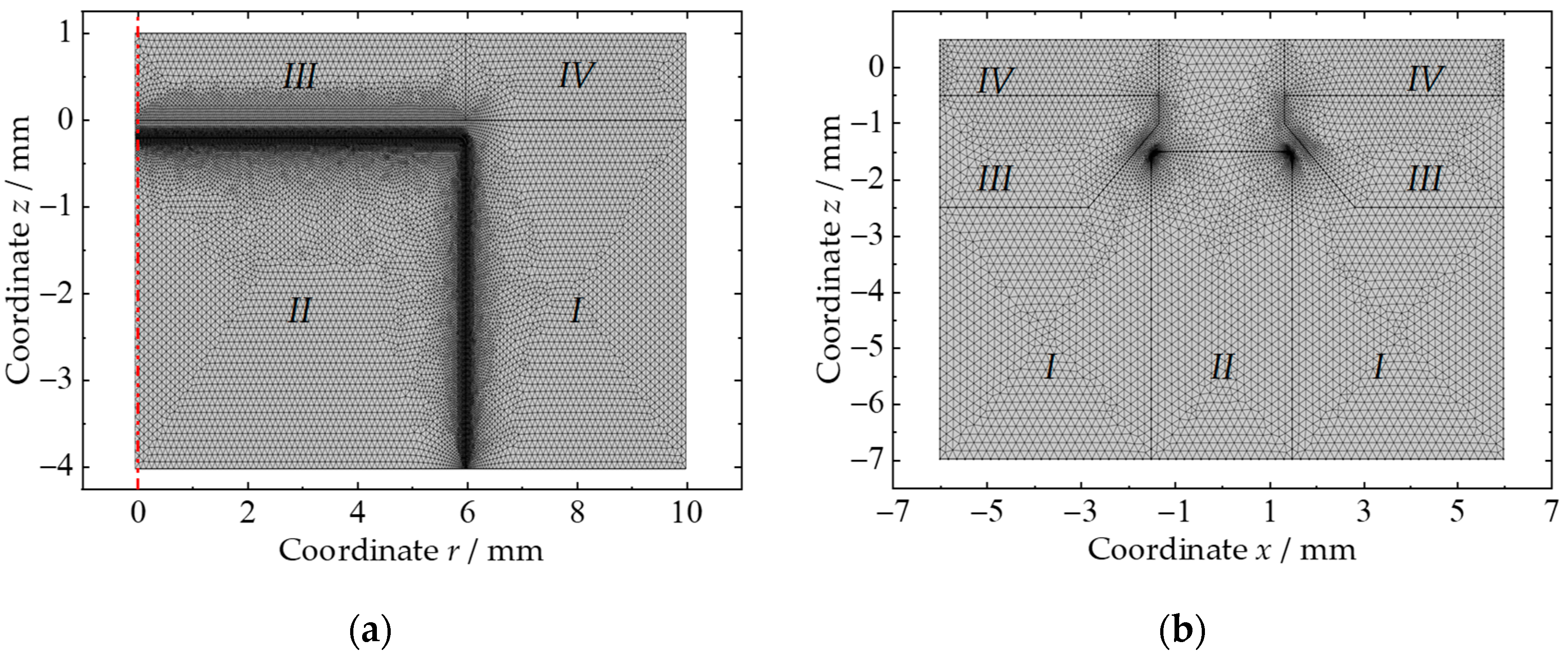
To achieve an accurate simulation, a robust meshing strategy is crucial. In this study, an automatic mesh generation algorithm within COMSOL Multiphysics was utilized. Specialized settings were configured to ensure that a minimum of 10 mesh elements were distributed along the working gap distance. Figure 4a,b depicts the initial meshes.
The mesh for the frontal gap experiments required a very fine resolution of the anode surface as strong distortions of individual mesh elements can occur here, particularly at the edges. Due to the dynamic changes in geometry during the simulation, the mesh experiences significant deformation. This can lead to unintended effects such as inverted mesh elements and reduced overall mesh quality. To avoid this, an automatic remeshing algorithm was used in the simulation process. This algorithm monitors the mesh distortion within the model domain. If the distortion of any element exceeds a predefined threshold of 0.8, the simulation pauses. Subsequently, the mesh undergoes a remeshing procedure, effectively restoring the mesh quality to an optimal state. Once the remeshing is complete, the simulation continues, ensuring accurate and reliable results.

4. Results and Discussion

4.1. Electrochemical Characterization

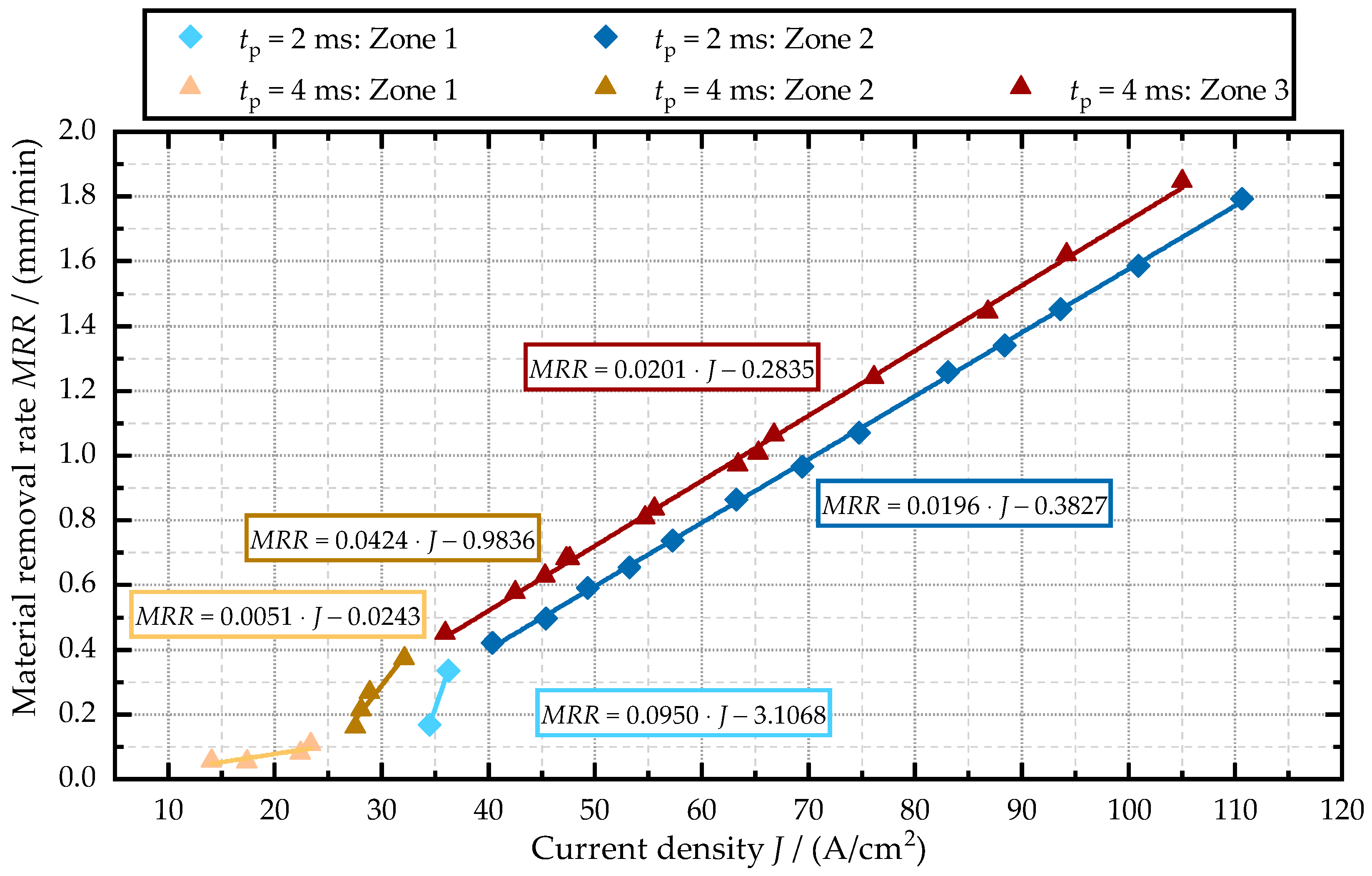
The resulting material removal rate for the material NiMnGa in sodium nitrate is shown in Figure 5. It can be recognized that with increasing current density, more material can be dissolved. When observing the material removal at 4 ms pulse length, it can be seen that within the investigated current density range between 14 A/cm2 and 105 A/cm2, three different trend lines can be highlighted. Especially above 35 A/cm2, the results show a very uniform dissolution behavior, which is underlined by the high coefficient of determination of 0.999. At 2 ms pulse length, only two zones are detectable, whereby above 40 A/cm2, a uniform ablation behavior occurs. These zones can be compared with zones 2 and 3 at 4 ms pulse length. Differences are attributed to the fact that longer pulse lengths contain more removal-active charges, resulting in a higher material dissolution compared to short pulses. At 2 ms pulse length, this leads to a reduced calculated removal rate of 0.099 mm/min. The impact of an oxide layer at the surface of the workpiece mentioned in Section 3.2 cannot be determined in more detail at present.

4.2. Validation of Simulation Approach

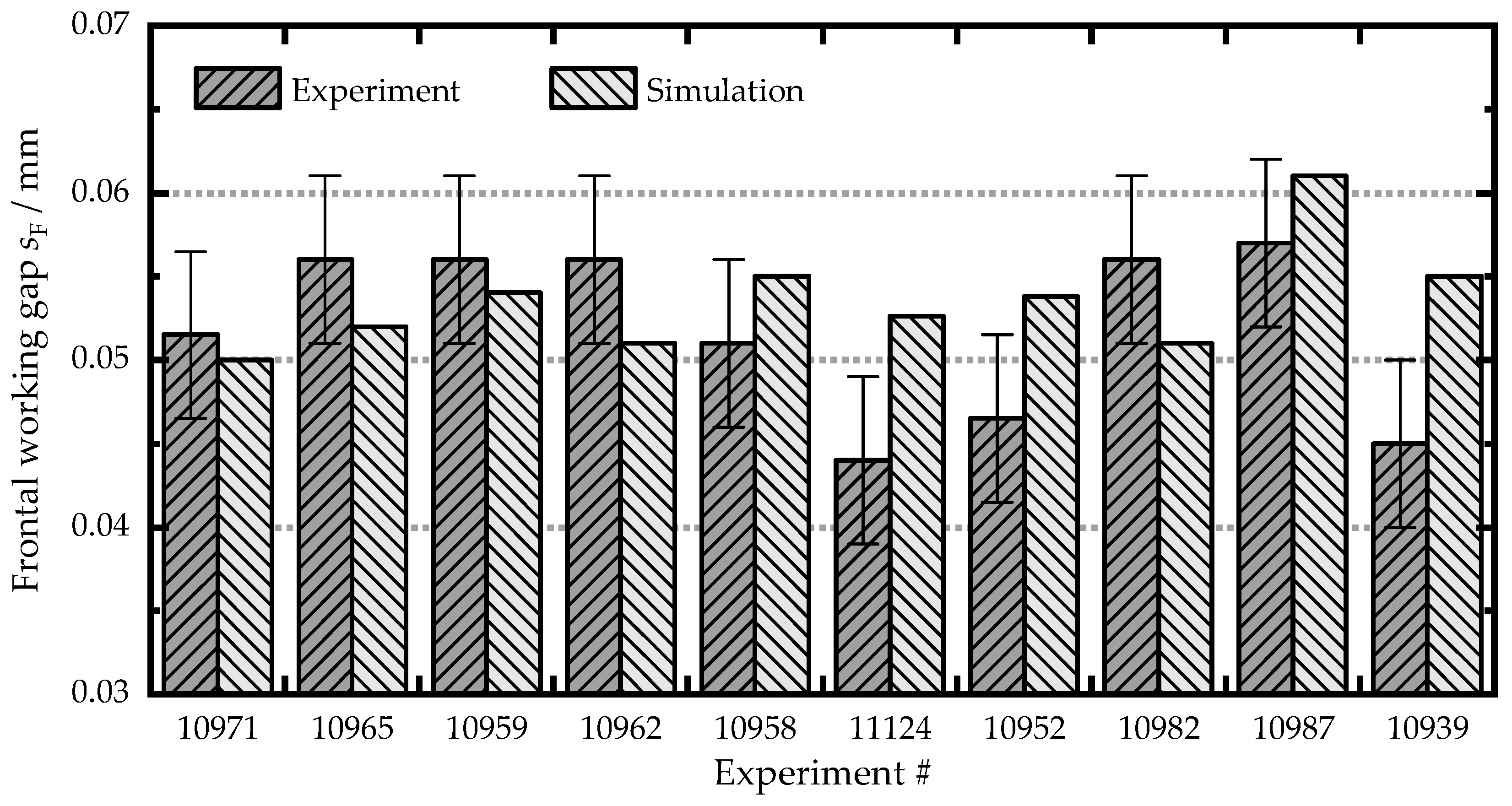
To validate the simulation approach, which includes the implementation of the material specific dissolution characteristics, the equilibrium frontal working gap sf is analyzed and compared with the experimental results. An equilibrium frontal gap is reached when the current is steady. This also indicates a stable state in the dissolution process. In Figure 6, a comparison is shown between the calculated and experimentally determined frontal working gaps. All relevant process parameters are outlined in Table A1 (Appendix A).
It is obvious that the experimentally determined frontal working gap values vary between 44 µm to 57 µm. On the other hand, the calculated frontal working gap ranges from 50 µm to 61 µm. Generally, the simulation aligns well with the experimental results. The largest deviation is observed for Experiment #11124, with a deviation of 8.6 µm. In summary, the simulation method is well suited for modeling the machining of MSM specimens; thus, tool and process design can be performed.

4.3. Simulation-Assisted Tool Design

As shown in Section 1, the simulation is used to answer different scientific questions regarding the influence of the geometrical design of the tool and insulation on the formation of the workpiece. For this purpose, the machining parameters of two different experiments are selected as examples. First, Experiment #10962 is chosen (see Table A1 in Appendix A; vf = 0.126 mm/min; f = 50 Hz; φ = 14 V; tp = 2 ms). On the other hand, Experiment #10939 is considered (see Table A1 in Appendix A; vf = 0.280 mm/min; f = 50 Hz; φ = 15 V; tp = 4 ms).
In Figure 7a, the workpiece formation for Experiment #10962 during a process time of 1200 s can be seen. At the beginning, the geometry is equal to the initial geometry, as shown in Figure 7b. After a process time of 250 s, the cathode moved a distance of about 0.525 mm in the negative z-direction, and in areas with current density values above 32 A/cm2, material dissolution takes place and the anodes’ shape changes according to the cathode shape, as seen in Figure 7b. As the process time increases, as shown in Figure 7c,d, the anode geometry, relative to the shape of the cathode, no longer changes, and an equilibrium working gap exists.
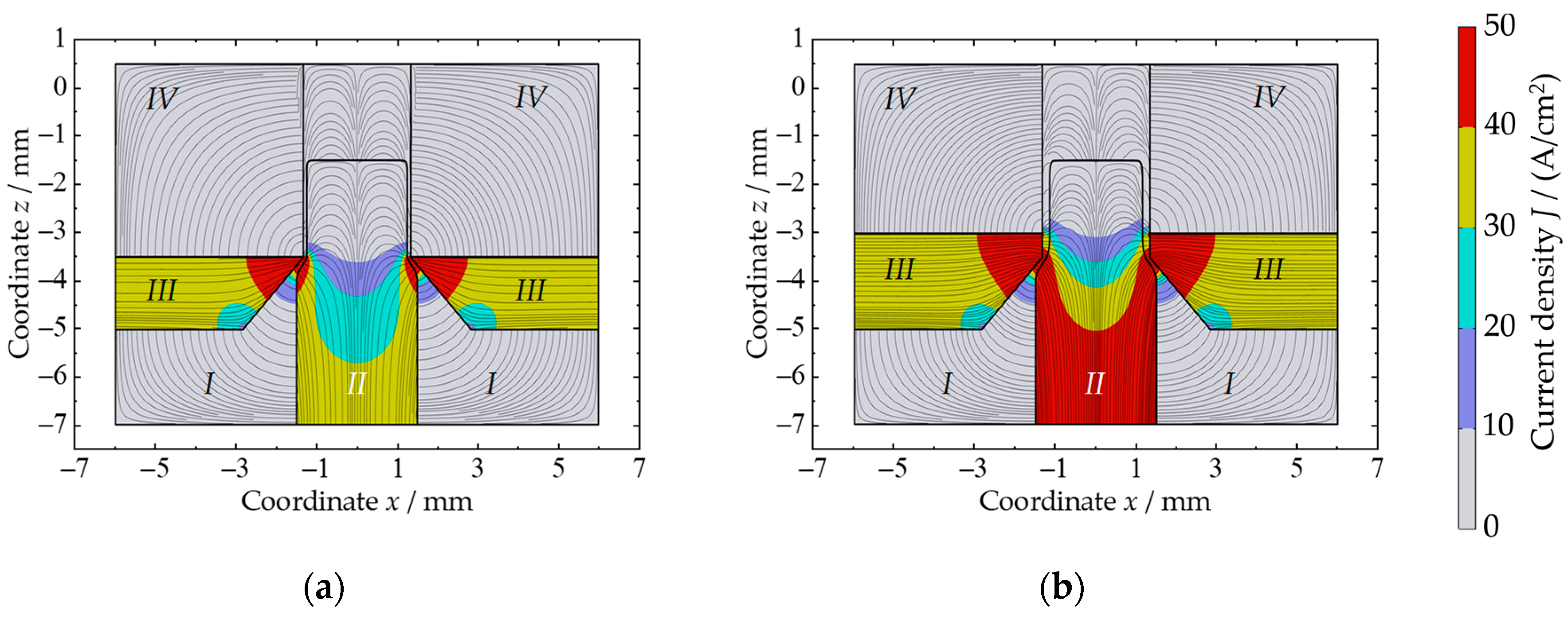
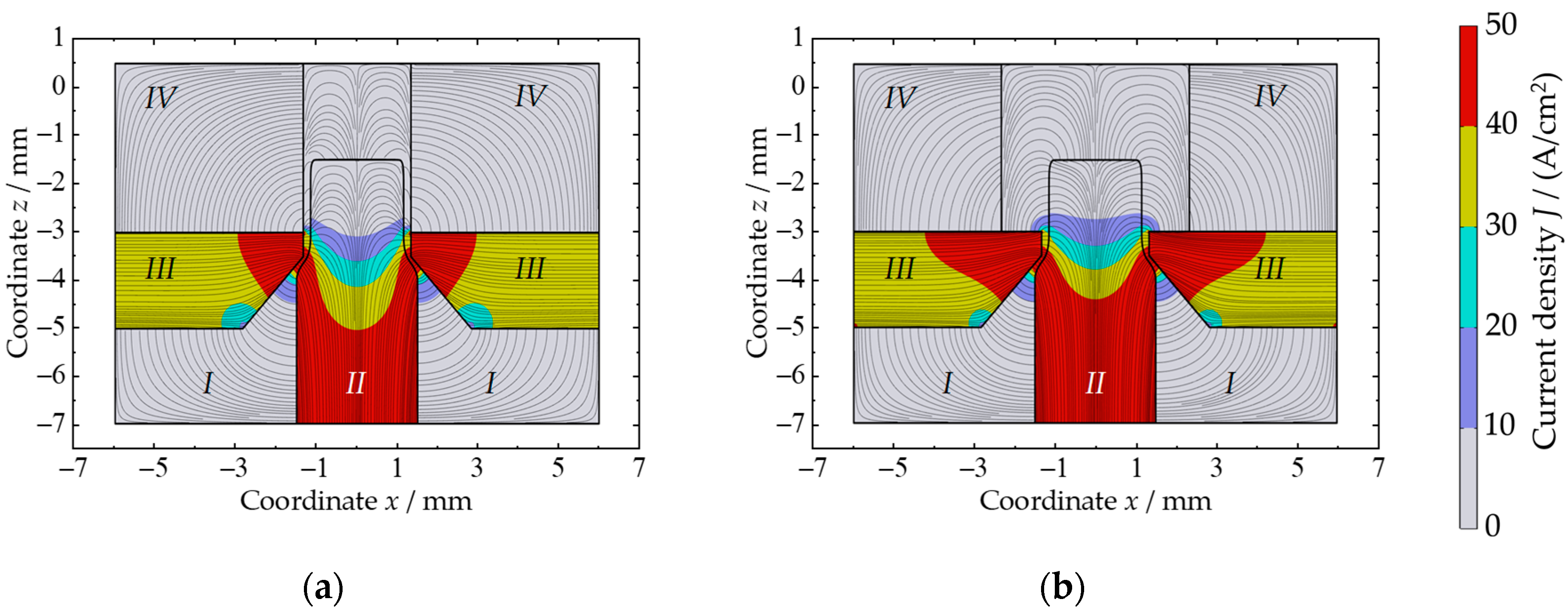
At this state, the final lateral working gap, according to Figure 1, can be derived. For this set of machining parameters, the final simulated lateral working gap is about 0.184 mm. As shown in Section 1 in the state of the art, a reduction or increase in the cathode surface area generally causes a change in the electrical charge exchange and thus extraordinarily influences the shaping of the workpiece. In Figure 8, the current density distribution (false color rendering) is shown for a height of the inner cathode surface of 0.01 mm (Figure 7a) and 0.5 mm (Figure 8b).
It can be seen that with increasing height, the current density distribution within the electrolyte (domain I) is more pronounced around the workpiece, and an increased stray current occurs in the area of the lateral working gap. In addition, the total current flow in the workpiece (domain II), indicated by a stronger red coloration, increases with the increasing height of the inner cathode surface.
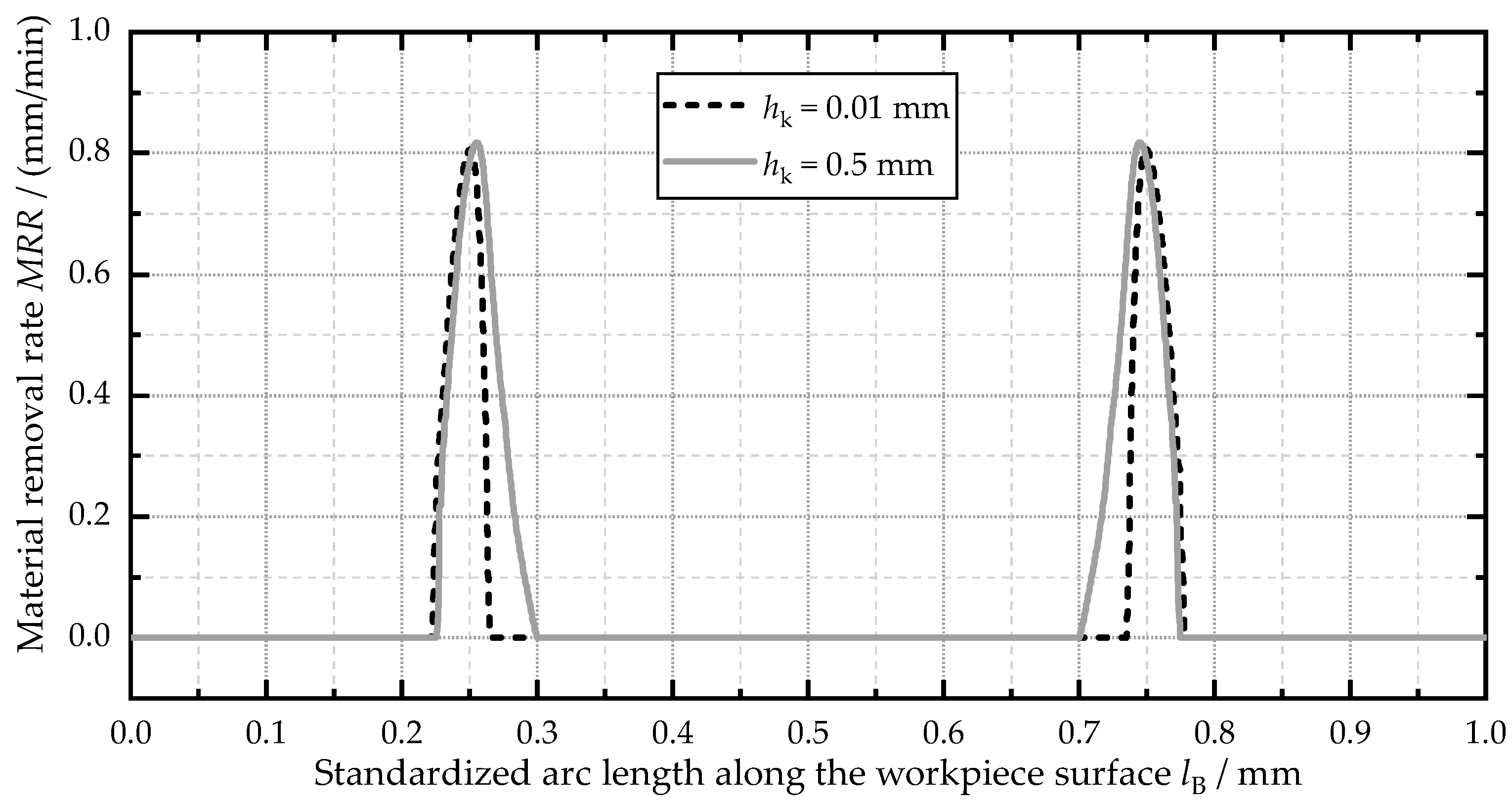
To analyze the influence of hk on the workpiece formation in more detail, the material removal rate MRR along the workpiece surface is plotted in Figure 9 for hk = 0.01 mm and hk = 0.5 mm after a simulated process time of 1200 s. The parameter lB is the arc length of boundary no. 3 and describes the perimeter of domain II (ref. to Figure 3b).
Due to the different resulting workpiece geometries, a direct comparison of the removal rate on the workpiece surface along lB is not possible for the parameter sets mentioned. For this reason, the standardized values of lB ranging from 0 to 1 are considered. Analyzing the results shown in Figure 9, it can be observed that the material removal rate increases at a standardized length of about 0.23 mm from 0 mm/min to a maximum value of approx. 0.81 mm/min for both heights considered. After that, the drop in material removal rate is significantly greater for hk = 0.01 mm compared to hk = 0.05 mm. This is a result of the smaller cathode height and, in consequence, a smaller current-carrying surface area, which leads to less charge transfer to the workpiece surface. In summary, it can be stated that the smaller height of the inner cathode surface leads to the more focused material removal along the workpiece surface, thus improving the localization of PECM.
By changing the design parameter doffset from 0 mm to 0.5 mm, the model geometry changes, and the upper surface of the cathode is not completely covered by insulation (domain IV). Figure 10a shows the electric current density distribution and current stream lines for Experiment #10962 with an offset of the insulation of 0 mm. In comparison, Figure 10b shows the same quantities but with doffset = 0.5 mm. It can be seen that with less insulation, the electric field changes and more current stream lines are present, starting from the top cathode surface and ending at the anode surface. This leads to an increase in stray current towards the anode, which will consequently influence the shape of the MSM-specimens. In a qualitative comparison, the influence of doffset appears to be lower than that of hk within the considered range.
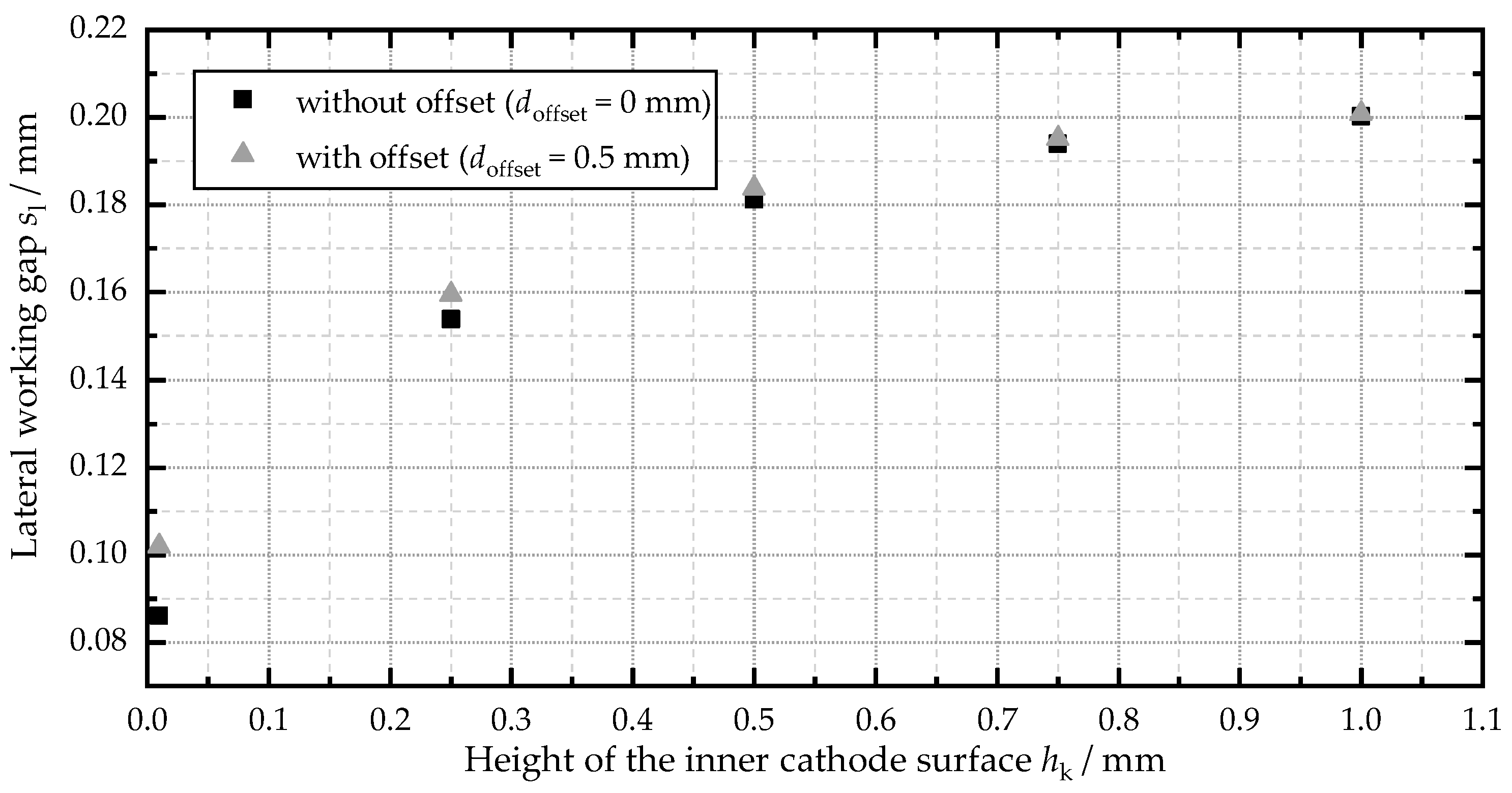
To quantify the influence of the parameters hk and doffset on the shape of the workpiece, two parameter studies were performed. In Figure 11 (Experiment #10962) and Figure 12 (Experiment #10939), the lateral working gap sl as a function of the height of the inner cathode surface for two different offset values of the insulation doffset can be seen. Based on the evaluation of the two diagrams, different findings can be observed. First, the lateral working gap increases with increasing hk for both considered experiments. But the increase reduces as the height of the inner cathode surface increases. Both findings can be explained by a combination of two different phenomena.
On the one hand, with bigger values of hk, the cathode takes more time passing a fixed point at the anode surface, thus increasing the actual dissolution time. This results in more metal dissolution and the growth of the distance between the cathode and the workpiece. On the other hand, following Ohms law, when the distance increases, the resistance becomes higher and leads to less metal dissolution of the workpiece, which explains the flattening curves. In addition to this, as soon as the current density value drops below the passivation limit of 32 A/cm2 for 4 ms and 36 A/cm2 for 2 ms (see Figure 5), the removal velocity becomes very low and no significant metal dissolution can take place anymore.
The second finding is that the lateral working gap is bigger when an offset between the insulation and the cathode is present. In the case of Experiment #10962, the lateral working gap increases by approx. 19% from 0.086 mm to 0.102 mm when the offset increases from 0 mm to 0.5 mm for hk = 0.01 mm. But the influence is no longer very pronounced as soon as the height of the cathode increases because of the decreasing ratio top cathode surface area (defined by the offset of the insulation) of the inner cathode surface area. In the case of Experiment #10939, the lateral working gap increases by approx. 29% from 0.113 mm to 0.145 mm when the offset increases from 0 mm to 0.5 mm for hk = 0.01 mm. This leads to the conclusion that if the charge-transfer increases due to the higher voltage of 14 V and longer pulse duration of 4 ms, the influence of the offset of the insulation will become stronger. So, the stray current is also increasing.
The conclusions of the simulation-based tool design are summarized as follows:
  • The height of the inner cathode surface hk has a significant influence on the lateral working gap sl and the current density distribution J.
  • The value of hk should be as small as possible to achieve a high accuracy.
  • The influence of the offset of the insulation doffset is relatively small but is dependent on the height of the inner cathode surface and the machining parameters.
  • The value of doffset should be as small as possible and homogenous around the top cathode surface.
It should be noted that production-related boundary conditions were not taken into account when creating the simulation model and therefore represent an idealization.

4.4. Fixture Development and Manufacturing

Based on the knowledge gained from the simulation, a customized removal fixture is developed to process one workpiece. One requirement of the application was the demand to manufacture two planes parallel in one step, classified as parallel processing. Nevertheless, a typical PECM fixture consists of several components, such as the following:
  • Alignment mechanism between the tool unit and the workpiece unit;
  • Stable, reproducible fastening of both electrodes (the cathodic poled tool and the anodic poled workpiece);
  • Precisely manufactured cut-out for defined ablative shaping;
  • Electrolyte guidance (in particular, a flow-optimized design of the electrolyte supply to ensure a uniform electrolyte flow at the process zone);
  • Electrical insulation for spatial limitation of the electrical fields and thus localization of the possible material dissolution.
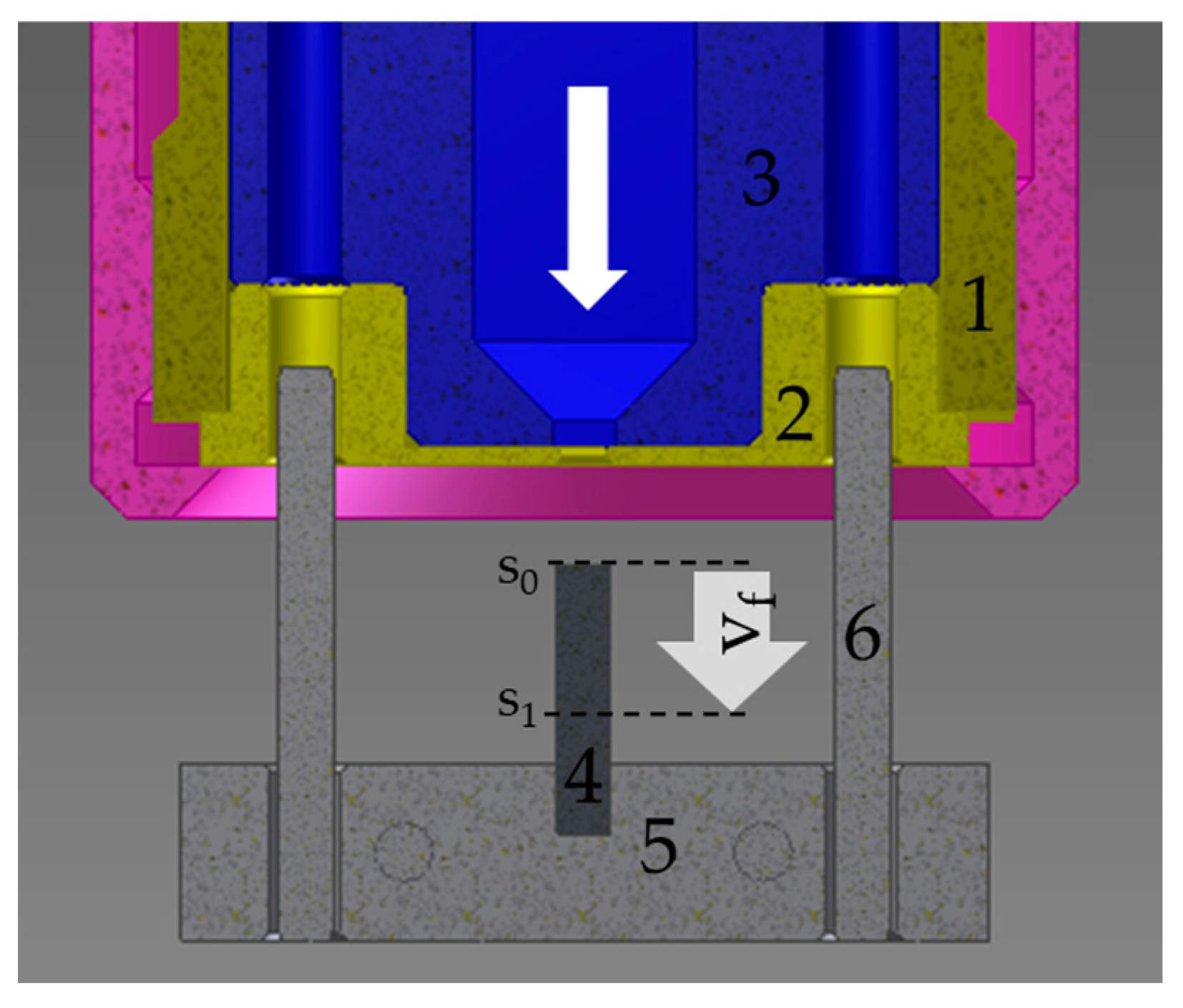
In accordance with the above-mentioned criteria, the CAD model with a sectional view of the developed fixture is shown in Figure 13. The components are named, adding the preferred choice of material. The material AISI 304 (EN: 1.4301) is an austenitic Cr-Ni-steel that exhibits good corrosion resistance in the electrolyte solution used. In addition, AISI 304 does not show hydrogen embrittlement induced by typical chemical reactions associated with hydrogen gas formation at the cathode’s surface [37,38]. POM is a technical plastic material which offers high durability and excellent electrical insulation properties.
The shaping process area of the fixture (cathode and insulation) creates increased challenges for the manufacturing realization. As approved in Figure 11 and Figure 12, the influence of the shaping height hk and the limitation of the electrical field by the offset between the cathode and the electrical insulation doffset play a vital role in the precise shaping. Figure 14a shows a design approach in which the electrical insulation and cathode are separately manufactured and assembled. Here, dimensional deviations between the insulation (blue) and cathode (yellow) can occur after mounting, whereby a resulting gap affects the workpiece dimensions. Alternatively, Figure 14b shows an electrically insulating insert (green, 1.0 mm thick) glued to the inside of the cathode (insert material: e.g., Araldite). This manufacturing solution can enable an insulation offset dOffset = 0.0 mm between the cathode and the electrical insulation. Although slightly higher expenses in the fixture manufacturing exists due to the additional insulation insert, components can be manufactured via micro milling.
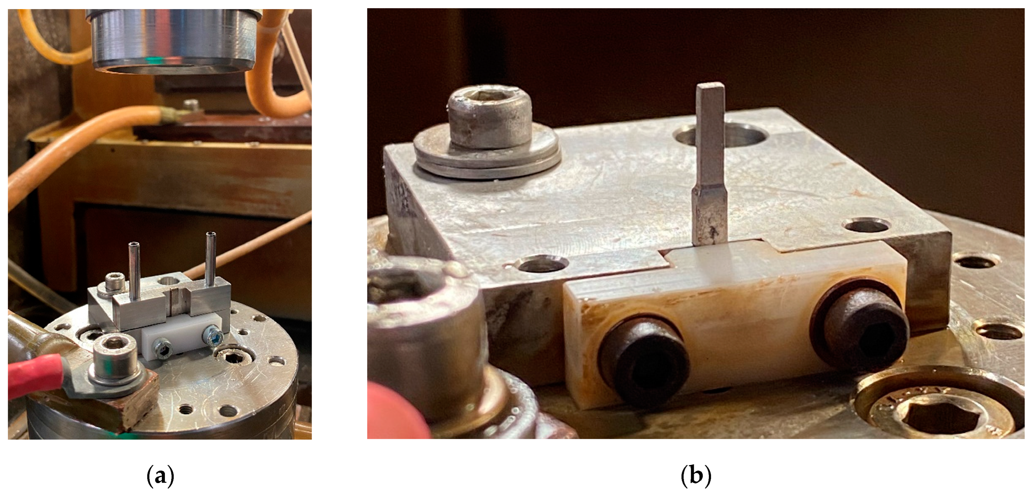
A fixture was manufactured at the Fraunhofer IWU using the solution approach shown in Figure 14a in order to test the initial configuration. As described, the electrically insulating electrolyte supply was mounted after finishing the cathode and insulation. A cathode shaping height hK of 0.45 mm and a rectangular cut-out of 2.67 × 1.67 mm were selected for the production of the cathode geometry. The installed fixture can be seen in Figure 15a, where an alignment tool is mounted to ensure that the tool and workpiece side are aligned in the X–Y spatial direction. This alignment tool was removed before the experiments were conducted. Figure 15b shows a specimen after the experiments.

4.5. Experimental Results of Simulation Machining with Developed Fixture

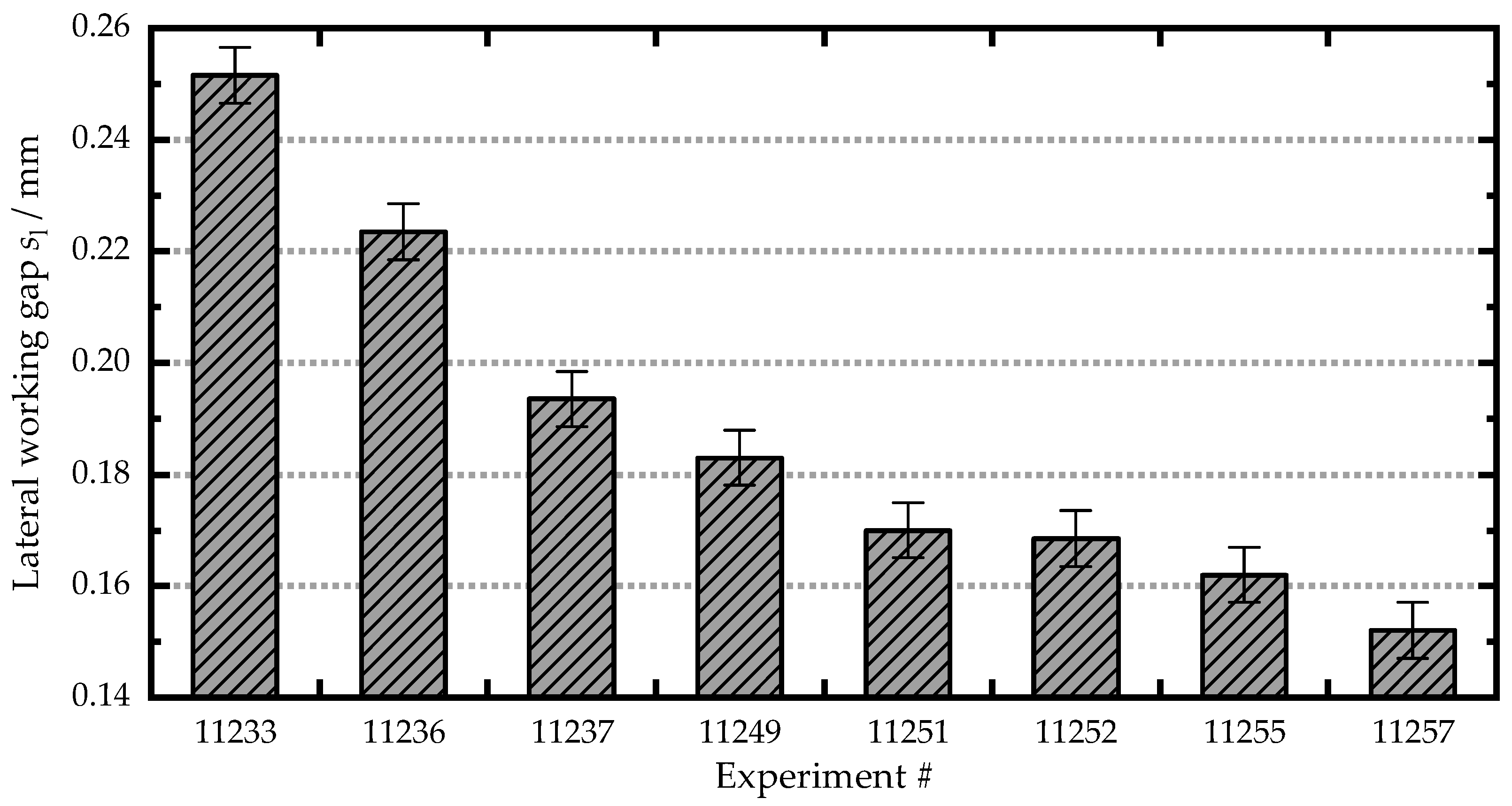
A series of experiments were conducted. The first series (1.1/11233 and 1.2/11236) was performed based on the results of the electrochemical material characterization. These guarantee short-circuit-free processing while ensuring a front working gap of 0.050 mm +/− 0.005 mm. The second test series (2.1/11237–2.6/11257) was carried out at a constant voltage and pulse length while increasing the feed rate until a front working distance of 0.025 mm after machining was reached. For a pulse length of 2 ms, this occurred at a feed rate of 0.30 mm/min. Figure 16 depicts the evolution of the final lateral working gap. The applied process parameters are attached in Table A2, Appendix B.
It becomes clear that the pulse length and feed rate have a strong influence on the resulting lateral working gap. Test series 1 (1.1 and 1.2) revealed a minimum lateral working gap of 0.223 mm for a pulse length of 4 ms (sf = 0.050 µm ± 0.005 mm). This was reduced even further with a shorter pulse length. In the second test series, a minimum lateral working distance of 0.151 mm was determined at a remaining front-working gap of 0.025 mm. A comparison of the simulation results shown in Figure 12 reveals a good correlation with the result of Experiment 1.2.
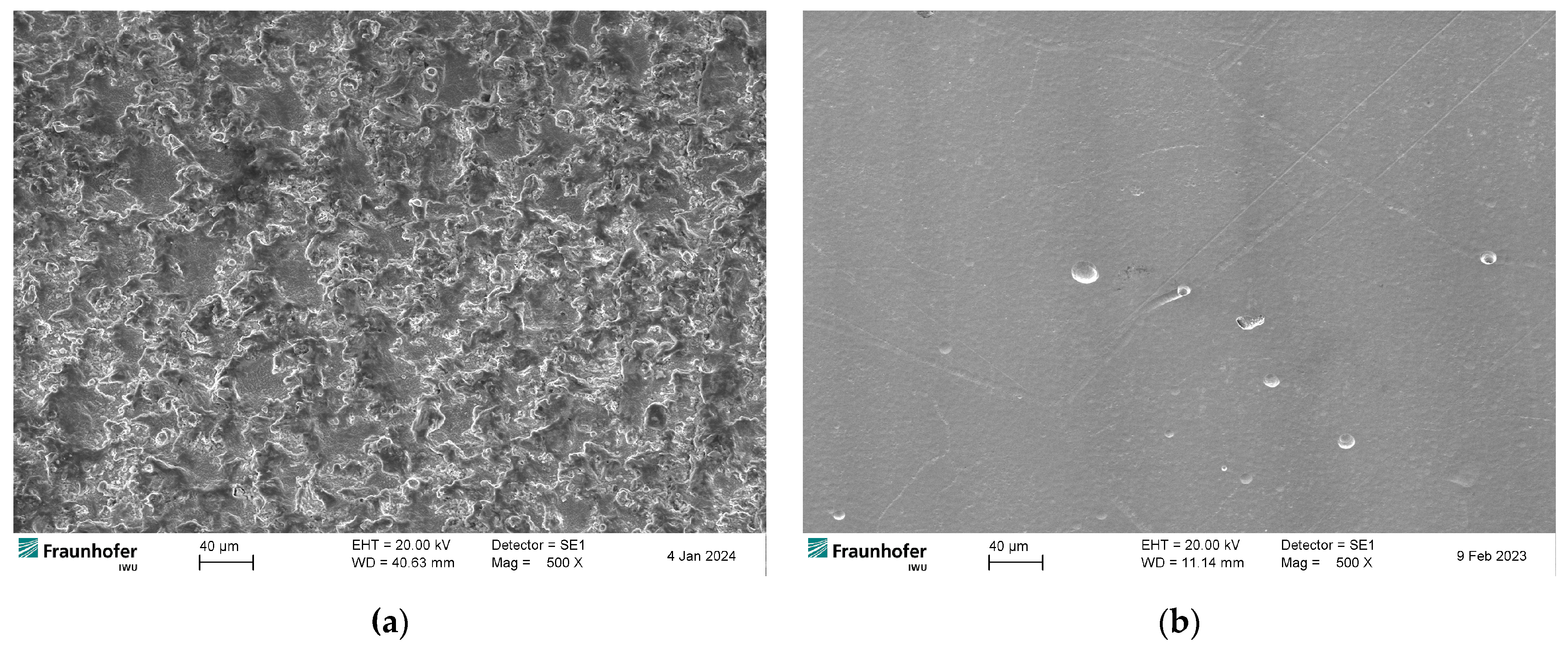
The evolution of the surface roughness and an analysis of the surface appearance using scanning electron microscopy were examined in more detail in another study [39]. For comparison of the surface appearance, Figure 17 allows for a qualitative evaluation by SEM at 500× magnification after preprocessing via EDM and finishing via PECM.
The left-hand Figure 17a shows the preprocessed condition after careful EDM processing. During thermal processing, a white layer forms on the surface as a reaction product. K. Oßwald studied AISI 4141 (42CrMo4) and showed that this white layer is inhomogeneous in thickness and has countless craters [40]. Analyzing the shape-memory alloy Nitinol, Liu et al. were able to confirm that the white layers have a crystalline instead of an amorphous composition [41]. Thus, it is expected that after EDM, the surface near material will not offer the necessary grain condition [39]. Consequently, this layer must be removed to ensure a homogeneous surface and the high dimensional accuracy of the specimens [42]. Compared to the right-hand Figure 17b, after PECM, a defect-free surface is revealed which uncovers only some pores of the base material. Scanning electron microscope examinations confirm that grain boundaries also remained unbroken.

5. Summary and Conclusions

This paper is dedicated to the simulation-assisted fixture design of an application for the precise finishing of the difficult-to-machine NiMnGa shape-memory alloy using pulsed electrochemical machining. State-of-the-art numerical simulation models are used to investigate two crucial influencing variables of the PECM fixture, namely, the shaping height and the electrical insulation on the top surface of the cathode, as well as the influence of the feed rate on the resulting lateral working gap.
The electrochemical material characterization of the NiMnGa shows a very good machinability in NaNO3. A stable dissolution behavior is already observed at low current densities, whereby this state was reached at 50 Hz and 4 ms pulse length at 36 A/cm2 and at 2 ms pulse length at 40 A/cm2. Differences are attributed to the fact that more removal-active charges are available at longer pulse lengths compared to short pulses.
The results of the simulation models show that the stray current is reduced by lowering the height of the cathode and minimizing the offset between the insulation and the cathode. The lateral working gap is also influenced by the stray current and increases by 20%, for example, if there is an offset of 0.5 mm between the cathode and insulation. Based on the simulation results, we may conclude that the height of the inner cathode surface should be kept as low as possible.
Once the fixture has been manufactured, its geometric dimensions are not changeable. For a still economically manufacturable shaping height hk of 0.45 mm, at 2 ms pulse length, an insulation offset of up to 0.5 mm shows a negligible influence. In contrast, switching to a pulse length of 4 ms, the shaping quality can decrease noticeably due to the given insulation offset. This can then be minimized up to a certain point by increasing the feed rate. Summarizing the experimental investigations of the pulse duration, voltage, and feed rate, the lateral working gap was adjustable between 150 µm and 250 µm.
Finally, PECM finishing removed surface defects such as the EDM-typical white layer and further defects from previous manufacturing steps. Only defined grain boundaries and very fine pores were found on the surface, which should not have any impact on the overall functionality.
Future work should be focused on exploring how precisely the simulation-based tool design for PECM can also be used for complex cathodes which require time-consuming 3D models. This may make the use of model order reduction unavoidable. Considering the findings on the impact of electrical insulation, the manufacturing challenges of the simultaneous machining of stainless steel and polymers also need to be solved. In addition, novel possibilities for cathodic electrical shielding should be verified. Although ECM is known for its cold and force-free manufacturing, it is nevertheless necessary to check whether process-induced influences on the crystal lattice or the ability to undertake shape transition can be fully excluded after the complete NiMnGa specimen has been machined.

Author Contributions

Conceptualization, F.B.; methodology, F.B.; software, F.B. and I.S.; validation, F.B. and I.S.; formal analysis, J.E. and A.S.; investigation, F.B. and I.S.; resources, F.B. and I.S.; data curation, F.B. and I.S.; writing—original draft preparation, F.B. and I.S.; writing—review and editing, All; visualization, F.B. and I.S.; supervision, F.B.; project administration, J.E.; funding acquisition, J.E. All authors have read and agreed to the published version of the manuscript.

Funding

This project is supported by the Federal Ministry for Economic Affairs and Climate Action (BMWK) on the basis of a decision by the German Bundestag. For administration, the AIF society is responsible for the program Joint Industrial Research (Industrielle Gemeinschaftsforschung). Grant number AiF IGF 22504 between Forschungsgemeinschaft Werkzeuge und Werkstoffe e.V. and Fraunhofer-Gesellschaft e.V. IWU.

Data Availability Statement

Data are contained within the article.

Conflicts of Interest

All authors declare no conflicts of interest.

Appendix A

Table A1. Process parameters used in the experiments for material characterization and simulation models.
Experiment IDTool Velocity
vf [mm/min]
Frequency
f [s−1]
Electric
Potential
φ [V]
Pulse Duration
tp [ms]
109710.030508.82
109650.0605010.52
109590.1005013.02
109620.1265014.02
109580.1505015.02
111240.020506.34
109520.070507.54
109820.130509.94
109870.1875012.14
109390.2805015.04

Appendix B

Table A2. Process parameters used in the lateral working gap experiments.
Experiment IDTool Velocity
vf [mm/min]
Frequency
f [s−1]
Electric
Potential
φ [V]
Pulse Duration
tp [ms]
1.1 (11233)0.1585014.04
1.2 (11236)0.2805015.04
2.1 (11237)0.1405015.02
2.2 (11249)0.1705015.02
2.3 (11251)0.2905015.02
2.4 (11252)0.2055015.02
2.5 (11255)0.2405015.02
2.6 (11257)0.3005015.02

References

  1. Vollmer, M.; Bauer, A.; Niendorf, T. Combined Shape Memory Alloy Phenomena: A Novel Approach to Extend Applications of Shape Memory Alloys. Mater. Lett. 2023, 347, 134643. [Google Scholar] [CrossRef]
  2. Molod, M.A.; Spyridis, P.; Barthold, F.-J. Applications of Shape Memory Alloys in Structural Engineering with a Focus on Concrete Construction—A Comprehensive Review. Constr. Build. Mater. 2022, 337, 127565. [Google Scholar] [CrossRef]
  3. Zhang, X.; Qian, M. Magnetic Shape Memory Alloys; Springer: Singapore, 2022; Volume 1200. [Google Scholar] [CrossRef]
  4. Behnken, H.; Hemes, S.; Pagounis, E.; Laufenberg, M. Thermal Stress and Local Crystallization Parameters in Single-Crystal Rods of Ni-Mn-Ga Ferromagnetic Shape Memory Alloys. J. Cryst. Growth 2020, 534, 125485. [Google Scholar] [CrossRef]
  5. Klocke, W.K.F. Fertigungsverfahren 3; Abtragen, Generieren und Lasermaterialbearbeitung; Springer: Berlin/Heidelberg, Germany, 2007. [Google Scholar]
  6. Wilson, J. Practice and Theory of Electrochemical Machining; Wiley-Interscience: New York, NY, USA, 1982. [Google Scholar]
  7. DeBarr, A.E.; Oliver, D.A. Electrochemical Machining; American Elsevier Pub. Co.: New York, NY, USA, 1968. [Google Scholar]
  8. Lohrengel, M.M.; Rataj, K.P.; Münninghoff, T. Electrochemical Machining—Mechanisms of Anodic Dissolution. Electrochim. Acta 2016, 201, 348–353. [Google Scholar] [CrossRef]
  9. Yu, C.Y.; Liu, C.S.; Huang, Y.H.; Hsu, Y.C.; Peklenik, J. The Investigation of the Flow Characteristics of the Gap in the Pulse Electrochemical Machining (PECM). CIRP Ann. 1982, 31, 119–123. [Google Scholar] [CrossRef]
  10. Zhang, Z.; De Meter, E.; Basu, S. Use of Bidirectional Electrolyte Flow to Improve PECM Uniformity. Int. J. Adv. Manuf. Technol. 2023, 127, 2843–2859. [Google Scholar] [CrossRef]
  11. Sneddon, S.; De Silva, A.K.M.; Gomez-Gallegos, A.A.; Jayasinghe, P. Precision Improvements in ECM via Tool Insert Development by 3D Printing. Procedia CIRP 2022, 113, 459–464. [Google Scholar] [CrossRef]
  12. Guo, J.; Zhu, D.; Zhu, D.; Hou, Z. Investigation of the Stray Corrosion of Inconel 718 at Low Current Density in NaNO3 Solution. Int. J. Adv. Manuf. Technol. 2023, 128, 3149–3159. [Google Scholar] [CrossRef]
  13. Davydov, A.D.; Volgin, V.M.; Lyubimov, V.V. Electrochemical Machining of Metals: Fundamentals of Electrochemical Shaping. Russ. J. Electrochem. 2004, 40, 1230–1265. [Google Scholar] [CrossRef]
  14. Rebschläger, A.; Kollmannsperger, R.; Bähre, D. Video Based Process Observations of the Pulse Electrochemical Machining Process at High Current Densities and Small Gaps. Procedia CIRP 2014, 14, 418–423. [Google Scholar] [CrossRef]
  15. Zong, Y.; Liu, J.; Zhu, D. Improving Blade Accuracy via Local Electrochemical Machining with Partial Insulated Cathodes. Precis. Eng. 2022, 76, 284–293. [Google Scholar] [CrossRef]
  16. Lu, J.; Riedl, G.; Kiniger, B.; Werner, E.A. Three-Dimensional Tool Design for Steady-State Electrochemical Machining by Continuous Adjoint-Based Shape Optimization. Chem. Eng. Sci. 2014, 106, 198–210. [Google Scholar] [CrossRef]
  17. Ernst, A.; Heib, T.; Hall, T.; Schmidt, G.; Bähre, D. Simulation of the Tool Shape Design for the Electrochemical Machining of Jet Engine Vanes. Procedia CIRP 2018, 68, 762–767. [Google Scholar] [CrossRef]
  18. Zhu, D.; Zhu, D.; Xu, Z. Optimal Design of the Sheet Cathode Using W-Shaped Electrolyte Flow Mode in ECM. Int. J. Adv. Manuf. Technol. 2012, 62, 147–156. [Google Scholar] [CrossRef]
  19. Li, Z.; Cao, B.; Dai, Y. Research on Multi-Physics Coupling Simulation for the Pulse Electrochemical Machining of Holes with Tube Electrodes. Micromachines 2021, 12, 950. [Google Scholar] [CrossRef]
  20. Zhou, S.; Wang, D.; Fu, T.; Zhu, D. Evolution of the Interelectrode Gap during Co-Rotating Electrochemical Machining. Metals 2023, 13, 1771. [Google Scholar] [CrossRef]
  21. Bortels, L.; Purcar, M.; Van den Bossche, B.; Deconinck, J. A User-Friendly Simulation Software Tool for 3D ECM. J. Mater. Process. Technol. 2004, 149, 486–492. [Google Scholar] [CrossRef]
  22. Volgin, V.M.; Lyubimov, V.V.; Davydov, A.D. Modeling and Numerical Simulation of Electrochemical Micromachining. Chem. Eng. Sci. 2016, 140, 252–260. [Google Scholar] [CrossRef]
  23. Temur, R.; Coole, T.; Bocking, C. Simulation of The Electrochemical Machining Process. In Proceedings of the 2001 International Solid Freeform Fabrication Symposium, Austin, TX, USA, 6–8 August 2001; pp. 486–496. [Google Scholar]
  24. Deconinck, D.; Van Damme, S.; Deconinck, J. A Temperature Dependent Multi-Ion Model for Time Accurate Numerical Simulation of the Electrochemical Machining Process. Part I: Theoretical Basis. Electrochim. Acta 2012, 60, 321–328. [Google Scholar] [CrossRef]
  25. Deconinck, D.; Van Damme, S.; Deconinck, J. A Temperature Dependent Multi-Ion Model for Time Accurate Numerical Simulation of the Electrochemical Machining Process. Part II: Numerical Simulation. Electrochim. Acta 2012, 69, 120–127. [Google Scholar] [CrossRef]
  26. Deconinck, D.; Hoogsteen, W.; Deconinck, J. A Temperature Dependent Multi-Ion Model for Time Accurate Numerical Simulation of the Electrochemical Machining Process. Part III: Experimental Validation. Electrochim. Acta 2013, 103, 161–173. [Google Scholar] [CrossRef]
  27. Ming, W.; Zhongninga, G.; Junfeng, H.; Xiaolei, C. Modeling and Simulation of the Material Removal Process in Electrolyte Jet Machining of Mass Transfer in Convection and Electric Migration. Procedia CIRP 2018, 68, 488–492. [Google Scholar] [CrossRef]
  28. Volgin, V.M.; Lyubimov, V.V.; Gnidina, I.V. Simulation of Ion Transfer during Electrochemical Shaping by Ultrashort Pulses; Springer International Publishing: Berlin/Heidelberg, Germany, 2019. [Google Scholar] [CrossRef]
  29. DIN SPEC 91399; Methode zur Bestimmung von Prozesseingangsgrößen für Das Elektrochemische Präzisionsabtragen—Anforderungen, Kriterien, Festlegungen. Deutsches Institut für Normung e.V.: Berlin, Germany, 2018.
  30. Meichsner, G.; Hackert-Oschätzchen, M.; Krönert, M.; Edelmann, J.; Schubert, A.; Putz, M. Fast Determination of the Material Removal Characteristics in Pulsed Electrochemical Machining. In Proceedings of the CIRP Conference on High Performance Cutting—HPC 2016, Chemnitz, Germany, 31 May–2 June 2016; Elsevier B.V.: Amsterdam, The Netherlands, 2016; Volume 46, pp. 123–126. [Google Scholar] [CrossRef]
  31. Xu, C.; Fang, X.; Han, Z.; Zhu, D. Wire Electrochemical Machining with Pulsating Radial Electrolyte Supply and Preparation of Its Tube Electrode with Micro-Holes. Appl. Sci. 2020, 10, 331. [Google Scholar] [CrossRef]
  32. Wang, J.; Xu, Z.; Wang, J.; Zhu, D. Electrochemical Machining on Blisk Channels with a Variable Feed Rate Mode. Chin. J. Aeronaut. 2021, 34, 151–161. [Google Scholar] [CrossRef]
  33. Hu, X.; Zhu, D.; Li, J.; Gu, Z. Flow Field Research on Electrochemical Machining with Gas Film Insulation. J. Mater. Process. Technol. 2019, 267, 247–256. [Google Scholar] [CrossRef]
  34. Meichsner, G. Entwicklung und Realisierung Einer Methode zur Bestimmung von Prozesseingangsgrößen für Das Elektrochemische Präzisionsabtragen; Technische Universität Chemnitz: Chemnitz, Germany, 2018. [Google Scholar]
  35. Lee, E.-S.; Shin, T.-H.; Kim, B.-K.; Baek, S.-Y. Investigation of Short Pulse Electrochemical Machining for Groove Process on Ni-Ti Shape Memory Alloy. Int. J. Precis. Eng. Manuf. 2010, 11, 113–118. [Google Scholar] [CrossRef]
  36. Rosenkranz, C. Elektrochemische Prozesse an Eisenoberflächen Bei Extremen Anodischen Stromdichten; Heinrich Heine Universität Düsseldorf: Düsseldorf, Germany, 2005. [Google Scholar]
  37. Ghasemiansafaei, M.; Schaefer, F.; Hall, T.; Baehre, D. Analysis of Mechanisms Affecting the Tool in Pulsed Electrochemical Machining. J. Electrochem. Soc. 2023, 170, 063504. [Google Scholar] [CrossRef]
  38. Bashkatov, A.; Hossain, S.S.; Mutschke, G.; Yang, X.; Rox, H.; Weidinger, I.M.; Eckert, K. On the Growth Regimes of Hydrogen Bubbles at Microelectrodes. Phys. Chem. Chem. Phys. 2022, 24, 26738–26752. [Google Scholar] [CrossRef] [PubMed]
  39. Böttcher, F. Investigations on the Surface Texture after Pulsed Electrochemical Machining (PECM) of the Magnetic Shape Memory Alloy NiMnGa. In Proceedings of the International Symposium on Electrochemical Machining Technology—INSECT, Saarbrücken, Germany, 13–14 November 2023. [Google Scholar]
  40. Oßwald, K.; Schneider, S.; Klink, A.; Bergs, T. White Layer Thickness Variation in Die Sinking EDM. Procedia CIRP 2022, 113, 5–9. [Google Scholar] [CrossRef]
  41. Liu, J.F.; Guo, Y.B.; Butler, T.M.; Weaver, M.L. Crystallography, Compositions, and Properties of White Layer by Wire Electrical Discharge Machining of Nitinol Shape Memory Alloy. Mater. Des. 2016, 109, 1–9. [Google Scholar] [CrossRef]
  42. Mwangi, J.W. Micro-Electrical Discharge Machining of Nitinol for Medical Applications; Chemnitz University of Technology: Chemnitz, Germany, 2019. [Google Scholar]
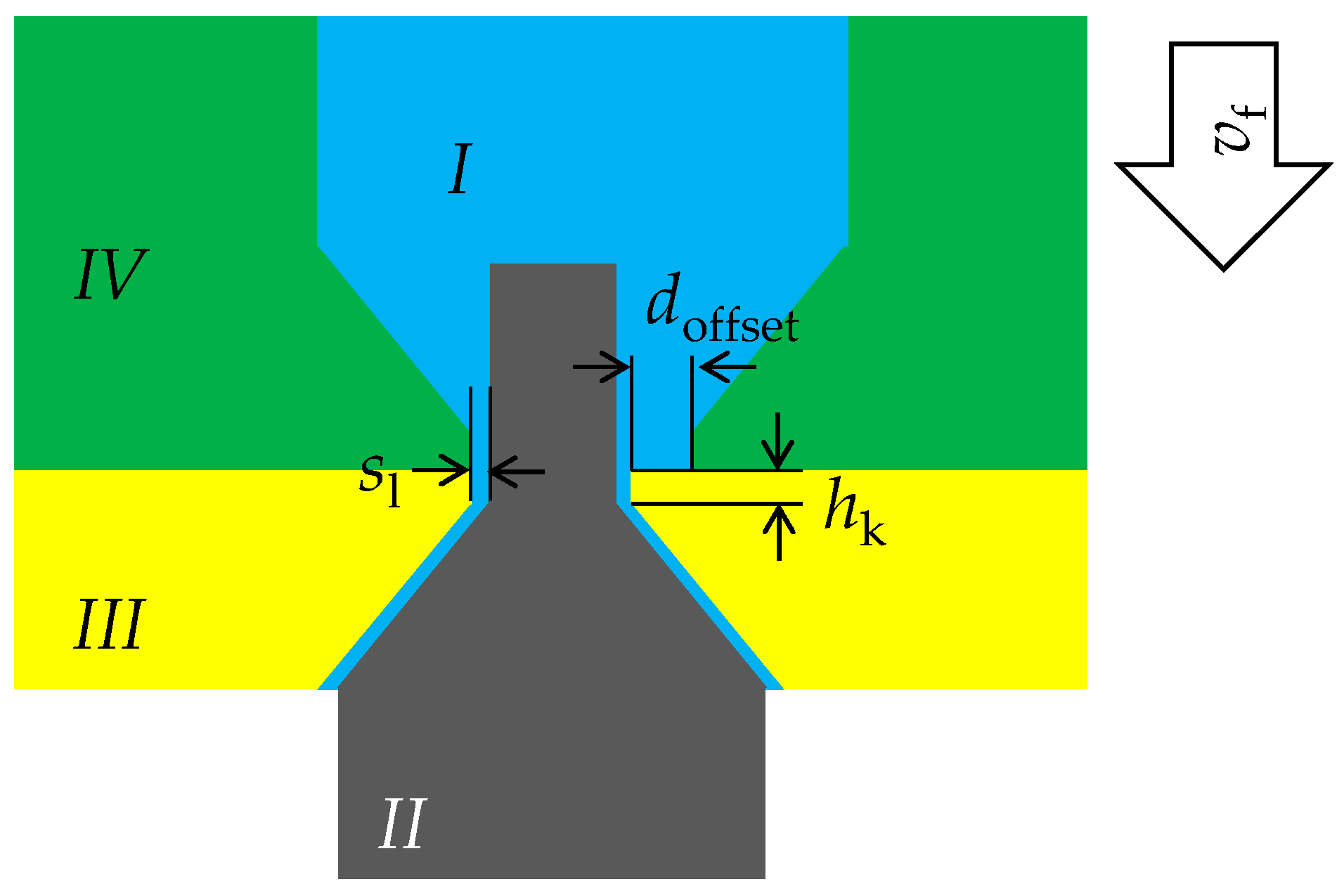
Figure 1. Conception of the studied geometrical features of this research for precise ECM. Area I is the electrolyte inflow area, area II the specimen, area III the shaping cathode and area IV the insulating material.
Jmmp 08 00046 g001
Figure 2. Simulation approach.
Jmmp 08 00046 g002
Figure 3. Simulation geometry: (a) frontal gap experiments; (b) machining process for manufacturing of MSM specimens. Material properties and boundary conditions are shown in Table 4, Table 5 and Table 6.
Jmmp 08 00046 g003
Figure 4. Initial mesh: (a) frontal gap experiments; (b) machining process for manufacturing of MSM-specimens.
Jmmp 08 00046 g004
Figure 5. Determined material removal rate MRR as function of the current density J for NiMnGa in NaNO3 solution.
Jmmp 08 00046 g005
Figure 6. Calculated frontal working gap sf compared to experimental results.
Jmmp 08 00046 g006
Figure 7. Model geometry and current density distribution during simulation of the NiMnGa machining process; stream lines represent current flow lines (uniform distributed). False color legend constant for all subfigures: (a) t = 0 s; (b) t = 250 s; (c) t = 850 s; (d) t = 1200 s.
Jmmp 08 00046 g007
Figure 8. Model geometry and current density J as false color rendering for Experiment #10962 after 1200 s simulated machining time. Stream lines represent current flow lines (uniform distributed): (a) hk = 0.01 mm; (b) hk = 0.5 mm.
Jmmp 08 00046 g008
Figure 9. Material removal rate MRR along the workpiece surface for different heights of the inner cathode surfaces hk for Experiment #10962. Arc length is standardized to a range from 0 to 1 for better comparison.
Jmmp 08 00046 g009
Figure 10. Model geometry and current density J as false color rendering for Experiment #10962 after around 1200 s simulated machining time; stream lines represent current flow lines (uniform distributed): (a) doffset = 0 mm; (b) doffset = 0.5 mm.
Jmmp 08 00046 g010
Figure 11. Side working gap sl as a function of the height of the inner cathode surface hk (Experiment #10962: vf = 0.126 mm/min; f = 50 Hz; φ = 14 V; tp = 2 ms).
Jmmp 08 00046 g011
Figure 12. Side working gap sl as a function of the height of the inner cathode surface hk (Experiment #10939: vf = 0.280 mm/min; f = 50 Hz; φ = 15 V; tp = 4 ms).
Jmmp 08 00046 g012
Figure 13. CAD cross-section view of the entire fixture for surrounding processing: (1) cathode holder (AISI 304); (2) cathode (AISI 304); (3) insulated electrolyte guidance (POM); (4) workpiece (NiMnGa); (5) workpiece holder (AISI 304); (6) guiding pins (AISI 304). The white arrow in (3) show the electrolyte flow direction.
Jmmp 08 00046 g013
Figure 14. (a) Shaping zone with insulating electrolyte guidance (blue). (b) Shaping zone with insulating electrolyte guidance (blue) and additional insulating insert (green).
Jmmp 08 00046 g014
Figure 15. Manufacturing of NiMnGa specimen: (a) alignment step before PECM; (b) NiMnGa sample after parallel processing by PECM.
Jmmp 08 00046 g015
Figure 16. Experimental results of the change of lateral working gap at increasing feed rates (according to Table A2, Appendix B).
Jmmp 08 00046 g016
Figure 17. Comparison of the surface texture at 500× magnification after preprocessing via EDM (a) and finishing via PECM (b).
Jmmp 08 00046 g017
Table 1. Chemical composition and calculated oxidation status of NiMnGa.
ElementNiMnGa
Volume content50.9%29.5%19.6%
Oxidation status223
Table 2. Constant parameters of the experiments.
Constant ParameterValue
Electrolyte solutionSodium nitrate NaNO3
pH value7.0
Temperature20.5 °C ± 1.0 °C
Electric conductivity72.0 mS/cm ± 0.5 mS/cm
Tool oscillationOn
Amplitude0.35 mm
Pulse frequency50 Hz
Start working gap0.05 mm
Table 3. Variable parameters during the experiments.
Variable ParameterValue
Voltage6 V to 17 V
Feed rate0.015–0.355 mm/min
Pulse length2 ms; 4 ms
Table 4. Material properties.
MaterialDomainCondition
ElectrolyteIσ = 7.2 S/m
NiMnGaIIσ = 106 S/m
AISI 304 SteelIIIσ = 106 S/m
PolyoxymethyleneIVσ = 10−10 S/m
Values according to Table A1 (Appendix A).
Table 5. Boundary conditions of electrodynamics.
ConditionBoundaryCondition
Electric potential1φ = φi − 5 V 1
Electric insulation4, 5, 6, 7-
Electric potential2φ = 0 V
Axial symmetry10-
1 Values according to Table A1 (Appendix A).
Table 6. Boundary conditions of the geometry deformation.
ConditionBoundaryCondition
Mesh Velocity8, 9vz = vz;i 1
Mesh Velocity3vn = va(Jn) 2
Mesh Displacement1, 2, 4, 5, 6, 7s = 0 mm
1 Values according to Table A1 (Appendix A). 2 Material-specific dissolution characteristics.
Disclaimer/Publisher’s Note: The statements, opinions and data contained in all publications are solely those of the individual author(s) and contributor(s) and not of MDPI and/or the editor(s). MDPI and/or the editor(s) disclaim responsibility for any injury to people or property resulting from any ideas, methods, instructions or products referred to in the content.