1. Introduction
Recent years have seen a growing interest in micro-machining. Important industrial sectors such as biomedical and automotive are the protagonists of this trend and have invested in these processes. Micro-machining finds applications in the manufacture of a wide variety of products such as medical components, micro-molds, electronics equipment, micro-electrical-mechanical system (MEMS), fluidic circuits and components, micro-valves, filters, actuators and subminiature motors.
Micro-machining includes the machining of parts or molds with overall dimensions less than 10 mm and dimensions of individual features less than 0.1 mm. With these dimensions, the smallest variation in the machining process due to the material machined, to the characteristics of the tool, to thermal variations in the machine or to vibrations can have a devastating impact on the process.
Micro-laser and micro-electrical discharge machining (EDM) are two very important technologies widely used in micro-machining.
They have several aspects in common. First of all, both use thermoelectric energy to remove material from the workpiece; they are non-contact processes, which makes them easy to produce micro-parts without distortion due to physical forces. The number of process parameters is relevant for both technologies. The laser can process many types of materials, from electrically conductive materials to non-conductive, while EDM can only process conductive materials. As regards milling applications, generally, a layer-by-layer removal process strategy is adopted for both technologies.
The laser technology represents a competitive solution for applications, such as micro-drilling, cutting, milling and texturing, thanks to the rapid development of short and ultra-short pulse laser technology (nano-pico and femtosecond regime), providing different operating wavelengths (from IR to UV) and excellent beam quality (TEM00 mode) [
1]. Depending on the chosen wavelength and configuration, laser sources are capable of directly machining a wide range of micron-scale features in a large range of materials, including metals, semiconductors, ceramics, hard materials, polymers and glasses [
2].
In recent years, ultrafast-pulse lasers (pulse duration shorter than a few picoseconds) were developed, offering advantages, especially in micro-machining. The use of ultrafast-pulse laser permits realizing the so-called “cold” ablation, which avoids thermal diffusion in the surrounding of the irradiated area, limiting the heat-affected zone, resulting in a very precise ablated volume without debris, damages and microcracks. Overall, therefore, ultrashort laser ablation of metals leads to a much higher quality compared to longer pulses [
3,
4,
5]. The laser milling technique allows for the ablation of a workpiece in order to realize on its surface cavities or features with various sizes and shapes in a controllable manner [
6].
In detail, a layer-by-layer removal process is realized by repeating a predefined scanning pattern a sufficient number of times until the required depth is reached. The micro-machining setup is schematically represented in
Figure 1.
The laser spot is moved over the scanning pattern in the x-y plane by a galvanometer scan head governed by a software system [
7]. The milling strategy, in terms of scanning geometry, has to be designed accordingly to the final geometry to be realized on the specimen [
8,
9].
The overall laser milling process involves a great number of parameters to be selected in order to assure a high-quality final processed material. They include the laser parameters, such as the operating wavelength, the pulse duration, the laser fluence and the repetition rate [
10,
11], and then the process parameters, such as the scanning speed, the overlap, the number of repetitions and the kind of scan pattern [
12].
Due to the inherent configuration of the laser milling process, the actual geometry achievable on the workpiece will inevitably feature a positive taper angle. This side effect can be partially tuned by applying special techniques and pieces of equipment (such as static beam inclination or dynamic precession mode ablation) [
13].
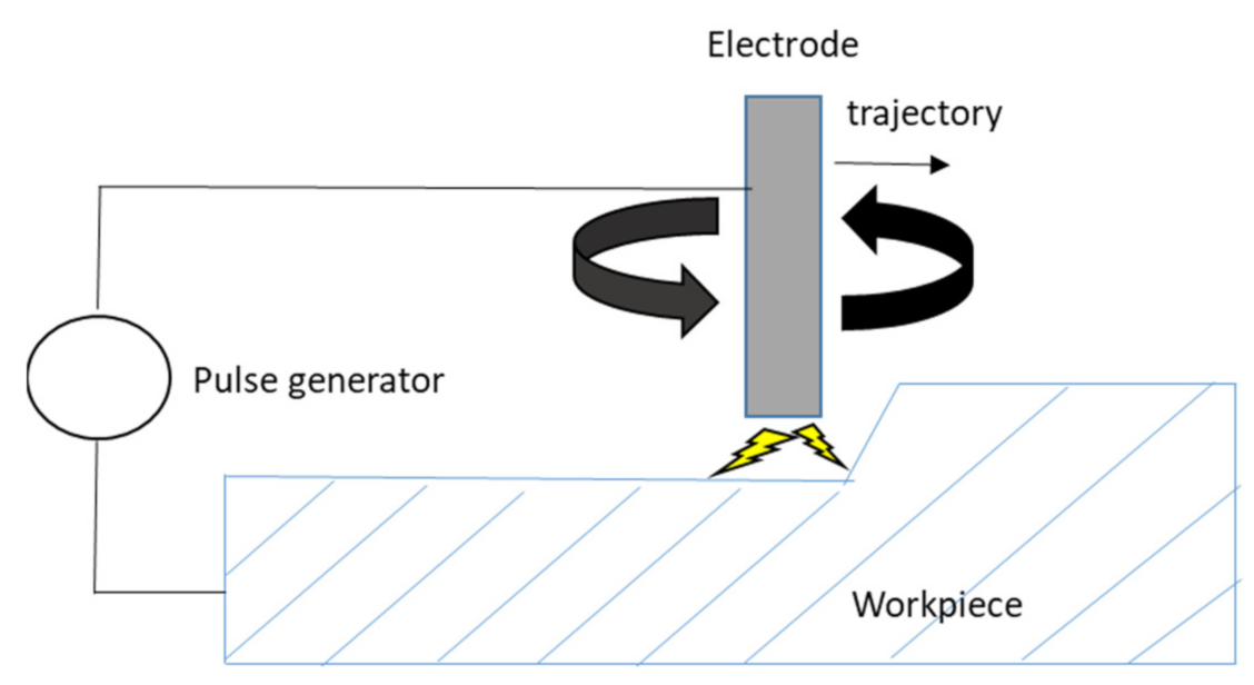
As regards micro-EDM technology, the material is removed by a series of rapid electric spark discharges between the cutting tool (electrode) and the workpiece. It is able to machine complex micro-parts of only conductive materials that traditional processes are unable to create [
14]. In fact, being a contactless process, there are very small machining forces between the electrode and the workpiece. This makes it easy to produce micro-parts without distortion due to physical forces. EDM is an ideal process for obtaining burr-free micro-size machined parts with a high aspect ratio using different materials. Micro-EDM milling can be applied to the production of 3D micro-cavities [
15,
16].
A scheme for EDM milling is reported in
Figure 2. The cylindrical tool, namely an electrode, follows a straight path to create straight profile channels with rectangular or square cross-sections. Unlike the laser technique, the EDM technique is affected by the electrode wear that must be taken into account. In fact, at the end of each milling path, the tool wears out, causing the tapering of the channel and a reduction in channel depth in the exit section compared to the entry section. Tool wear compensation techniques are used to obtain the correct path geometry [
17,
18,
19]. Moreover, during the machining, the electrode tip changes shape assuming a non-uniform radial dimension for a certain length. This is called electrode shape deformation. It was demonstrated that, from the point of view of the electrode changing shape, different phases occur during the erosion process due to the change in the position of the highest intensity of the electrical field [
20]. Moreover, the transversal wear of the electrode causes a taper rate in machining. The taper increases as the electrode diameter increases, as reported in [
21].
Not only straight channels can be precisely machined using the EDM milling operation, but also particular micro-features can be machined. Semi-circular, circular, zigzag and free-form micro-features are also possible through CAD integration with the CAM system to generate the required toolpath plan [
22,
23].
Several parameters both electrical and not electrical are involved in the EDM process (
Figure 3) [
24]. The process performance is evaluated using indicators, such as the material removal rate (MMR), the tool wear ratio (TWR), the taper rate (TR) and the surface characteristics (surface roughness, remelting layer thickness, thermally altered zone).
The influence of the process parameters on the performance in micro-EDM machining is widely dealt with in the literature, while the comparison between machining technologies is poorly reportedSome studies on this topic are available but are focused primarily on micro-drilling [
25,
26]. In these studies, the influence of the process parameters for both laser and EDM on the micro-drilling performances was underlined. Moreover, it was found that laser is more competitive than EDM as regards MRR despite the accuracy of the micro-holes in terms of dimensional accuracy (overcut, taper rate and circularity). As regards the micro-geometrical characteristics of the inner surface of micro-holes, the smoothness of the generated surfaces is better using ultrashort pulsed laser than micro-EDM [
27]. Some authors proposed hybrid solutions using both technologies to increase efficiency in micro-drilling applications [
28,
29].
A wider comparison among different technologies for micro-machining was made in [
30], but EDM was considered only for drilling applications.
The aim of this work is to compare laser and EDM technologies in a micro-milling application. A femto-laser and a micro-EDM system were used for this scope. Two different milling geometries were selected as case studies: micro-channel and micro-pillar at two aspect ratios. The tests were executed on stainless steel, titanium alloy and aluminum. The selection of the process parameters for both technologies was made after preliminary tests. The performance was evaluated considering the machining time and the macro- and micro-geometrical characteristics of the obtained features. The comparison of the results underlined the strengths and weaknesses of the two technologies. This work can contribute to improving the knowledge of the capability of femto-laser and EDM in a micro-milling application and can assist the decision-making stage of the selection of technology in the production field as a function of the characteristics of the micro-components that have to be produced.
2. Experimental Plan
A comparison between the femtosecond laser micro-machining and the EDM technology was made on two different milling geometries, as schematically represented in
Figure 4. The first one, reported in
Figure 4a, consists of a micro-channel milled on stainless steel AISI316L, titanium alloy Ti6Al4V and aluminum Al5754-H111 with a length L
0 = 10 mm, a width of about t
0 = 0.1 mm and depth of about Δ = 0.1 mm. The second one consists of a matrix of micro-pillars, based on the geometry reported in
Figure 4b, milled on AISI316L and Ti6Al4V. The pillars featured a top diameter D
0 = 2r
0 = 0.05 mm and two different heights of about Δ = 0.05 mm and Δ = 0.1 mm.
As already discussed in the Introduction, the actual geometry achievable on the workpiece has a positive taper angle that, for the geometries reported in
Figure 4, translates into the geometries depicted in
Figure 5.
Table 1 summarizes the details of the experimental campaign.
The femto-laser tests were performed at the company Kirana (Trento, Italy). The laser milling was carried out using a femtosecond laser system featuring a Pharos PH1 (Light Conversion, Vilnius, Lithuania) laser source with a 260 fs pulse duration, fundamental wavelength λ = 1030 nm and maximum repetition rate of 606 kHz. The laser beam was focused on the workpieces by using an excelliSCAN 14 (SCANLAB, Puchheim, Germany) with an F-Theta lens (focal length f = 100 mm). With the system thus configured, the laser spot focused on the samples has a diameter of 20 µm. The spot overlap was set to 60% because this value ensures a high ablation efficiency and, in the meantime, a high-quality sample, avoiding surface thermal damage [
10]. Generally, the optimum fluence to be applied to operate in a highly efficient ablation regime has to be about 7.5 times the threshold fluence [
10]. Considering this and the need to perform the layer-by-layer ablation in a gentle regime, to maintain a good surface quality [
31], the operating mean laser fluence applied in the process is for aluminum, steel and titanium alloy 0.65, 0.6 and 0.55 J/cm
2, respectively. The laser ablation was performed in air at room temperature.
The tests executed using the EDM machine were made at the Laboratory of Micro Technologies of the University of Bergamo. The Sarix-SX200 is available as a micro-EDM system using hydrocarbon oil as the dielectric. EDM is characterized by several process parameters, and the optimization phase plays a key role in obtaining, in general, good performance. In general, EDM system constructors give suggestions for the selection of the parameters. In this work, several preliminary tests were made to optimize the machining conditions. One of the most important parameters is the Energy that defines the impulse shape and the level of violence of erosion—in other words, the adopted strategy to remove material (roughing, finishing, fine finishing). The choice of the energy is a tradeoff between the machining accuracy and the machining time. The type of erosion affects both the performance in terms of material removal rate (MRR) and tool wear ratio (TWR) and the accuracy of the machining. Considering the types of applications studied, in this test, it was decided not to test big impulses (roughing) but the fine ones (finishing). Other important parameters are peak current, voltage, frequency, width, which is the time the transistor remains active, gain, which is a parameter that controls the gain of the reaction block, and gap, which is a value proportional to the distance between the electrode and the workpiece during erosion. Finally, regulation identifies a certain regulation management algorithm defined by the machine manufacturer. As the electrode, a cylinder tungsten carbide electrode was chosen with a diameter equal to 0.1 mm. The optimized process parameters used in the EDM experiments are reported in
Table 2.
3. Analysis of the Results
In this section, the results for both technologies are descripted. Data about the performance of the process and the geometrical characteristics of the obtained features are reported. The geometrical characterization was made using a Zeiss EVO 40 scanning electronic microscope (SEM) and a white light interferometer. The white light interferometry permits reconstructing the 3D shape of the specimens, and the analysis was performed with a SmartWLI interferometer (GBS, Ilmenau, Germany) featuring a 20× Mirau objective with a numerical aperture NA = 0.4 and a resolution of 10 nm along the vertical axis and 0.48 µm in the x-y plane.
3.1. Femto-Laser
Table 3 reports the geometrical data of the channel realized on the three different samples through the laser milling technique. Moreover, it shows the calculated MRR, taper and the bottom profile roughness Ra.
The machining time depends on the milling strategy and also on the specific physical and electronical characteristics of the machined specimen. Among these properties, the material density covers a determinant role. Indeed, in this case, the lower machining time occurs for aluminum, allegedly due to its low density (2.75 g/cm3), whereas the maximum machining time occurs for steel (8.0 g/cm3), followed by the titanium alloy (4.5 g/cm3). Since the ablated volumes of materials are quantitatively comparable, the MRR of aluminum results to be almost more than twice that of the other two metals.
As regards the geometrical characteristics, the taper rate is not negligible as the walls of the channels come with an angle of about 16° for the three machined samples. This is an inherited feature of the laser engraving process, which causes the side walls to deviate from the expected orthogonal direction and present an inclination. The formation of inclined sidewalls is ascribable to a series of factors that characterize the process, as the divergence of the laser beam [
32], the overlap [
33], and the gaussian beam profile [
13]. This side-effect can be reduced by properly optimizing the process parameters [
32] but cannot be completely eliminated unless optical components are used to vary the angle of incidence of the laser beam on the cavity walls [
13].
The roughness of the bottom layer depends on the process parameters, as a too high applied fluence can induce the presence of fused areas with bumps, or a too low overlap can produce ripples on the surface. The laser milling process has been optimized to reduce the machining time, reach the highest efficiency and maintain a good surface quality. A good agreement was found by maintaining the bottom profile roughness of less than 0.35 µm for the three machined samples.
Figure 6 shows optical microscopy images of the channel for the three materials, and
Figure 7 shows the 3D reconstruction of the aluminum sample.
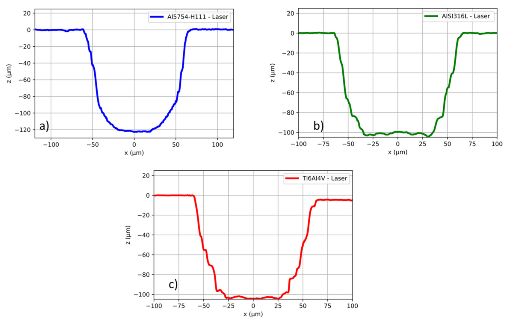
The three channels present a clean and precise profile at the top, and the bottom is uniform and mainly flat. Their profiles were sampled with white light interferometer, and the resulting curves are shown in
Figure 8.
The aluminum channel profile presents a more rounded curve compared to those of steel and titanium, where a well-defined trapezoidal shape is visible. In these last two, the profile presents some steps in the order of 2–3 µm; these constitute a slight deviation from the ideal profile.
Arrays of pillars with different heights, respectively, of about 50 µm and 100 µm were realized on steel and titanium specimens. Their characteristic geometrical values, as well as, taper and MRR are shown in
Table 4.
As seen in the previous case, comparing the two materials, titanium needs less time to be machined (approximately 10% less) for both the 0.05 mm and the 0.1 mm depth.
The pillars present a well-defined circular top face with a diameter of about 50 µm, as highlighted in the SEM images reported in
Figure 9 and in the 3D shape reconstruction in
Figure 10. Additionally, for this geometry, the pillar walls present a positive taper; this, as previously discussed, is an intrinsic side effect of the laser-milling micro-machining process. The walls slop remains constant, and the perimeter of the bottom face of the pillar enlarges as the height increases, leading to a smaller calculated taper for the higher pillars. In conclusion, the two specimens subjected to this micro-machining process show a comparable MRR value as found for the micro-channels.
3.2. Micro-EDM
Table 5 reports the EDM process performance in terms of material removal rate and the electrode wear. Geometrical data are also reported.
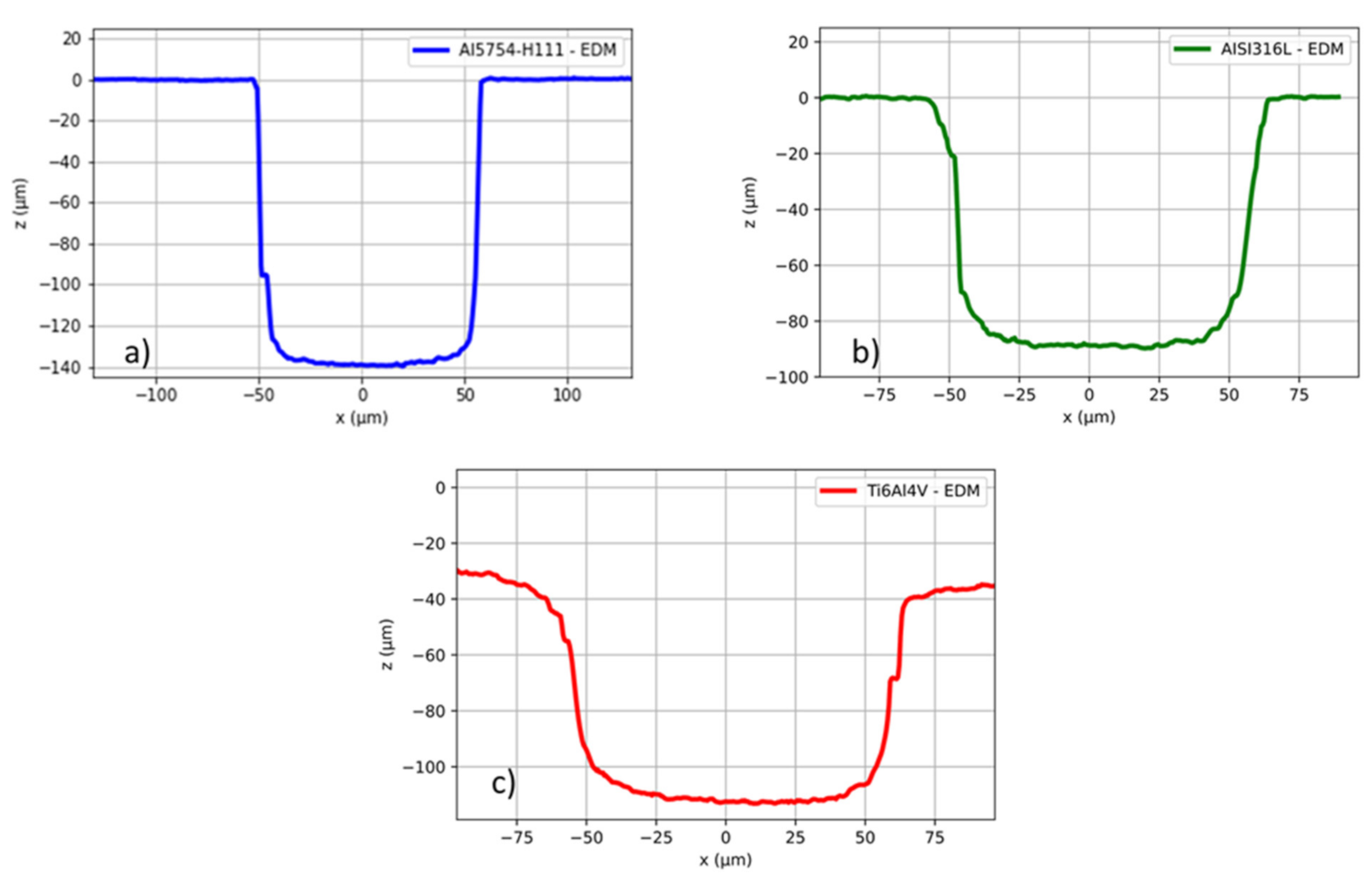
Figure 11 shows optical microscopy images for the three materials. Among the three materials, the maximum MRR occurs for aluminum, while stainless steel and titanium alloy reach a similar value. These differences are mainly due to the physical and electrical properties of the workpiece material. The machined workpiece influences the entity of the electrode wear that seems to be proportional to the erosion time. The machining gap and the run-out of the electrode produces differences among the samples’ widths. Additionally, the taper rate is almost very low, and the walls of the channels are vertical. The edges are sharp and well defined; only in one case, the resolidified material on the surface is present (see titanium). Stainless steel and titanium alloys have a higher taper rate (over 0.4) than aluminum. This result can be justified considering two aspects. First of all, the machinability of the material: increasing the machinability of the workpiece material, in other words decreasing the machining time, the side sparks that enlarge the holes are less. Second, the electrode wear: when decreasing the machining time, the tip of the electrode is affected by a lower shrinkage. As regards the roughness, this index can be related to the dimensions of the craters that could be influenced by the thermal and physical properties of the workpiece material. Melting point and thermal conductivity are higher for aluminum, and the craters are larger despite of the roughness index.
The samples were characterized with white light profilometer, and the reconstructed 3D of the aluminum samples and the profiles of the three specimen are, respectively, reported in
Figure 12 and
Figure 13.
As regards the pillars,
Table 6 shows the data obtained using EDM technology. The geometric data are the mean value.
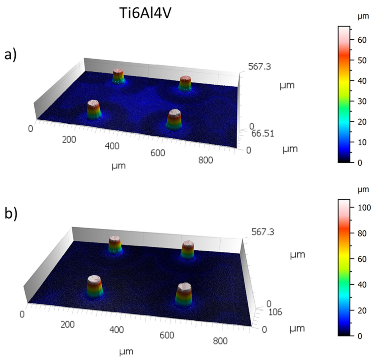
Figure 14 shows SEM images of the pillars for each tested conditions, and in
Figure 15, two 3D reconstructions of the pillars realized on the titanium alloy are reported. With a fixed workpiece material, the effect of the depth of the pillars is clear: the electrode wear is proportional to the machine depth, as the MRR is almost constant; increasing the depth, the material removal occurs with the same feed, and the top and bottom dimensions of the pillars are similar; therefore, the taper rate is around the double at a depth of 50 µm than 100 µm.
Comparing the two materials, titanium needs less time to be machined, and consequently, the electrode wear is also lower than that obtained when stainless steel is machined. The taper rate is higher for the titanium. This behavior can be explained considering the side discharges that have a lower time to erode the lateral surfaces.
To conclude, in all cases, the top pillars show a good circularity and very low taper.
4. Comparison Femto-Laser and EDM Performance
In this section, a comparison of the femto-laser and EDM performance obtained to fabricate micro-channels and micro-pillars was made.
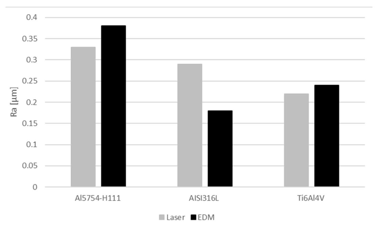
Figure 16,
Figure 17 and
Figure 18 regard the 100 µm channels machining in terms of MRR, taper rate and roughness bottom profile, respectively. From the point of view of the MRR, the laser removes the material one order of magnitude faster than EDM. EDM permits obtaining a machining that has better geometrical characteristics than laser. It can be noted that when stainless steel and titanium is machined, the difference of the taper rate between the two technologies is not high, but it is useful to remark that, in these cases, channels EDM present a lower depth compared to those realized via the femto-laser technique, causing a higher taper rate. Finally, as regards the surface roughness, the workpiece material affects the comparison of the two technologies: when stainless steel is machined, EDM reaches a better surface finishing, while for the other materials, the values are similar.
In
Figure 19 and
Figure 20, the performance comparison of the pillars machining is reported in terms of MRR and taper, respectively. The trend found for the machining of micro-channel is confirmed also for the pillar’s geometry: laser, with respect to EDM, realizes a fast material removal. In terms of geometrical accuracy, the pillar taper rate is smaller for the EDM, and it can be seen that for higher pillar depth, the taper tends to decrease.
These results give a contribution in the definition of the capabilities of the femto-laser and EDM in micro-milling applications. In fact, from this analysis, the limits and the strengths of a femto-laser and EDM in micro-milling applications were highlighted. Both the technologies ensure a good accuracy of the machining. The femto-laser permits obtaining very fast machining despite the walls tapering, while EDM is the opposite. The results showed that the proper technology selection contributes to improving the quality of the manufacturing production. The optimal choice of the manufacturing system is a function of the geometries and tolerances of the feature to realize.
5. Conclusions
This paper compares two different technologies, femto-laser and EDM, to realize two micro-features on different metals: channels and pillars. Both the technologies use thermal energy to remove material, but the removal material mechanism is different. The milling geometries were machined at two aspect ratios when it was possible on three workpiece materials: aluminum, stainless steel and titanium alloy. The performance was evaluated considering the material removal rate and the geometrical characteristics of the obtained micro-features. In both the features, laser reaches an MRR an order of magnitude faster than EDM but with a lower geometrical accuracy in terms of the walls’ tapering.
The EDM technique, in the range of the performed test, is not limited in the sample reachable depth. Conversely, the maximum depth achievable by means of the femto-laser milling method is strongly dependent on the positive taper angle that affects the cavity walls: the feasible geometries have to present an aspect ratio that considers this characteristic in order to be realized.
If the specimen to be machined is conductive, the choice between the two techniques to be applied in an industrial context has to be done by taking into account the results of the research. The factors that have to be analyzed are the amount of material to be ablated, the required geometrical accuracy as well as the time at the disposal for the machining. If a high accuracy of the machined sample is required, and the necessary machining time is acceptable for the amount of the volume to be removed, the choice can fall in the EDM technique. In contrast, whether the processing involves a higher volume to be removed, and in the meantime, the sidewalls taper is acceptable for the required geometry, the femto-laser milling technique can be applied.
This paper highlights the limits and the strengths of femto-laser and EDM, improving their knowledge in specific applications. The presented results could help the actors involved in the micro-machining to select the best technology as a function of the specific target.

 ,
, 


