Abstract

UV Light-Induced Response Degradation Characteristics of Silicon-Based Detectors †

X-FAB Global Services GmbH, Haarbergstraße 67, 99097 Erfurt, Germany
*
Authors to whom correspondence should be addressed.
Presented at the XXXV EUROSENSORS Conference, Lecce, Italy, 10–13 September 2023.
Proceedings 2024, 97(1), 230; https://doi.org/10.3390/proceedings2024097230
Published: 25 September 2024
(This article belongs to the Proceedings of XXXV EUROSENSORS Conference)

1. Introduction

High energy radiation is known to potentially impact silicon-based optical sensors adversely, either permanently or reversibly. We have studied the impact of UV light (190–300 nm) concerning the spectral response of silicon photodiodes.
We found that the first and obvious prerequisite for degradation is a sufficiently high quantum efficiency in the energy range that the light may damage. If the light is already absorbed before it reaches the silicon, or if the detector has no sensitivity, due to its junction design, both lead to degradation-free devices. Most of the silicon detectors in use today are of such kind and are “immune” to UV-caused degradation, due to their poor UV response capabilities.
Nevertheless, there are special use cases where the detection of short wavelength light (below 300 nm) is required and for these, the degradation is to be avoided or at least known [1].

2. Materials and Methods

To generate UV light, mercury lamps are mostly used, but they provide a poorly defined energy spectrum (see Figure 1). In publications concerning the subject of degradation, often an intensity value per area is given without a complete spectrum. The wavelength at which the stress is provided and at what intensity remains unknown. A mercury lamp does not stress at all wavelengths of the spectrum.
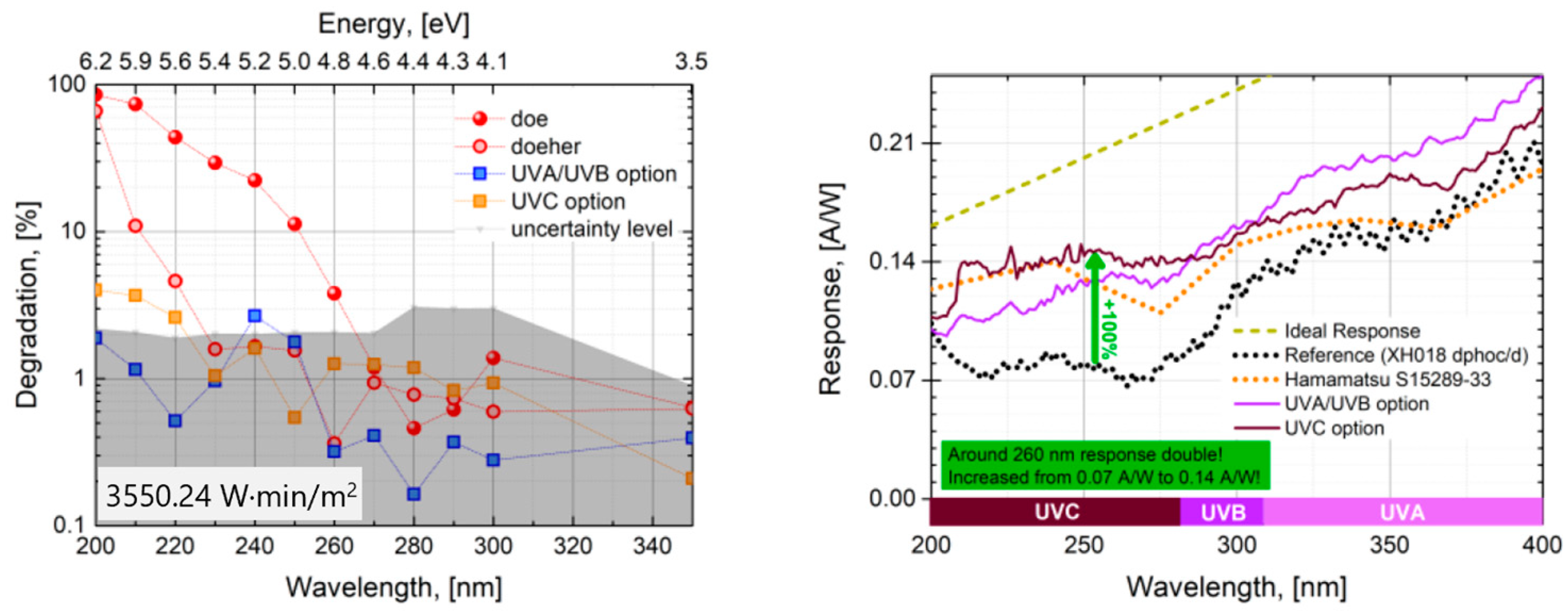
To investigate the potential damage, we use a laser driven light source from Energetiq, a monochromator, and a solarization robust fiber for illumination. By that, we characterize the photon-energy-related degradation (see Figure 2, left).

3. Discussion

3.1. Spectral Dependency of UV Caused Degradation

It was expected that shorter wavelength light has higher degradation potential. This behavior is affirmed. Interestingly, we see no significant damage for wavelengths longer than 300 nm, and around 280 nm, the degradation is not a steady function of photon energy. This very likely originates from the refractive index properties and the high reflection around these wavelengths.

3.2. Exceptional High UVC Response

It is a challenge to engineer sensors with high UV response without degradation. Based on our long experience [3], we can show silicon sensors with UV response down to the vacuum UV (200 nm), which show very little degradation and can be used for sensing applications in that special range. Our newest research shows a significant response improvement (see Figure 2, right) for the spectral range around 260 nm, which is important for the application of disinfection.

4. Patents

Three patents are pending to protect the IP used to realize the new silicon photodiode with exceptional high UV response.

Author Contributions

D.G., conceptualization, methodology, original draft preparation, visualization, review and editing. P.F.S., software, validation, formal analysis, investigation, data curation, writing. All authors have read and agreed to the published version of the manuscript.

Funding

This research received no external funding.

Institutional Review Board Statement

The work was internally discussed and approved by X-FAB for external publication.

Informed Consent Statement

Not applicable.

Data Availability Statement

Raw data related to the measurements of the photodetectors shown here are available. Specimens of all different fabricated photodetectors as well as demonstration kits can be provided to interested parties under individual agreements.

Conflicts of Interest

Both authors were employed by the company X-FAB Global Services GmbH.

References

  1. Yampolsky, M.; Pikhay, E.; Roizin, Y. Embedded UV Sensors in CMOS SOI Technology. Sensors 2022, 22, 712. [Google Scholar] [CrossRef] [PubMed]
  2. Education in Microscopy and Digital Imaging. Available online: https://zeiss.magnet.fsu.edu/articles/lightsources/mercuryarc.html (accessed on 1 March 2023).
  3. Gäbler, D.; Henkel, C.; Thiele, S. CMOS integrated UV-Photodiodes. 30th EUROSENSORS. Procedia Eng. 2016, 168, 1208–1213. [Google Scholar] [CrossRef]
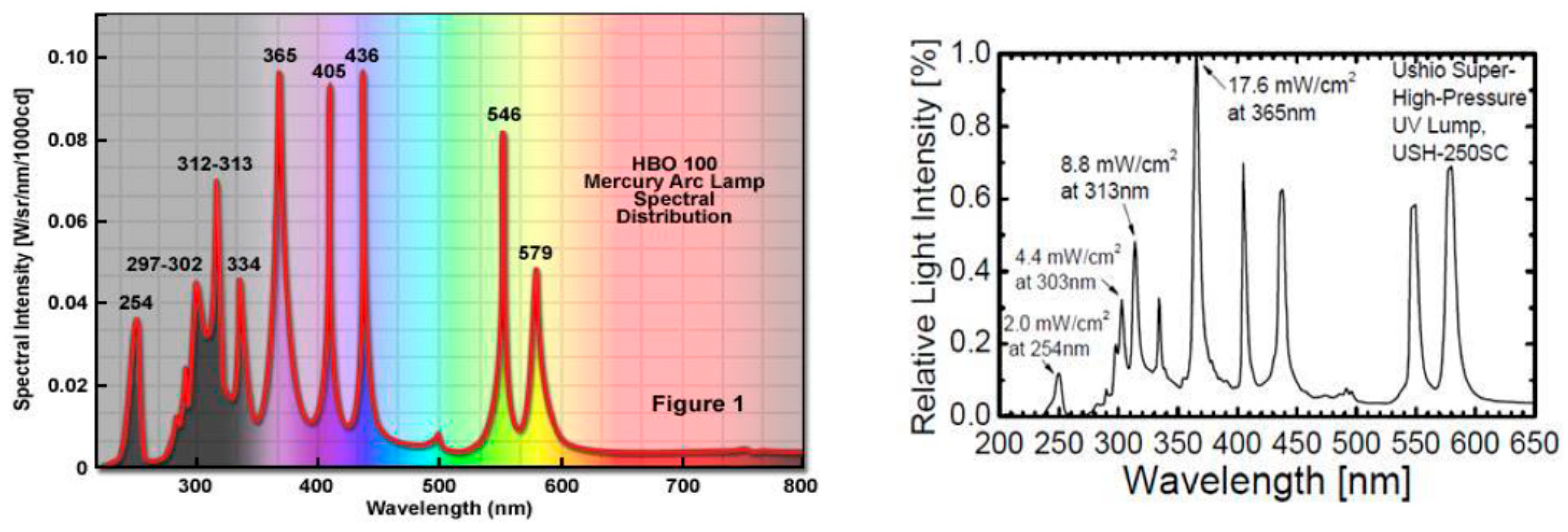
Figure 1. Intensity spectrum of a first mercury lamp (HBO 100) [2] and a second mercury lamp (UV-Eraser with Grid Lamp G750NO2).
Proceedings 97 00230 g001
Figure 2. (left): Photon-Energy related UV degradation for the case of two typical photodiodes (doe and doeher, not specialized on UV robustness), compared to two UV specialized devices, all manufactured in a 0.18 µm CMOS process, with epi wafer material. Dashed lines serve solely as a guide to the eye to observe the data tendency. (right): High sensitivity UVC response achieved by a CMOS integrated device (Technology XS018) compared to a reference CMOS device (Technology XH018) and a discrete backside illuminated device (Hamamatsu).
Proceedings 97 00230 g002
Disclaimer/Publisher’s Note: The statements, opinions and data contained in all publications are solely those of the individual author(s) and contributor(s) and not of MDPI and/or the editor(s). MDPI and/or the editor(s) disclaim responsibility for any injury to people or property resulting from any ideas, methods, instructions or products referred to in the content.