Abstract

Merging Surface Plasmon Optical Detection with Electronic Sensing †

Laboratory for Life Sciences and Technology (LiST), Faculty of Medicine and Dentistry, Danube Private University, 3500 Krems, Austria
Presented at the XXXV EUROSENSORS Conference, Lecce, Italy, 10–13 September 2023.
Proceedings 2024, 97(1), 196; https://doi.org/10.3390/proceedings2024097196
Published: 19 April 2024
In one of the “classical” configurations of electrolyte-gated field effect transistors (EGOFETs) for biosensing, the planar gate electrode is functionalized by (a monolayer of) receptors, to which the analyte molecules of interest bind from the analyte solution, thereby modifying the gate potential, which in turn modifies the source drain current as the sensor output signal.
This format inspired us to attach a prism to this Au gate electrode, mounting this to a surface plasmon spectrometer in the Kretschmann configuration coupled to a flow cell, thus allowing for simultaneous optical and electronic sensing of the identical affinity reaction, happening in real time at the sensor Au surface (Figure 1, [1]).
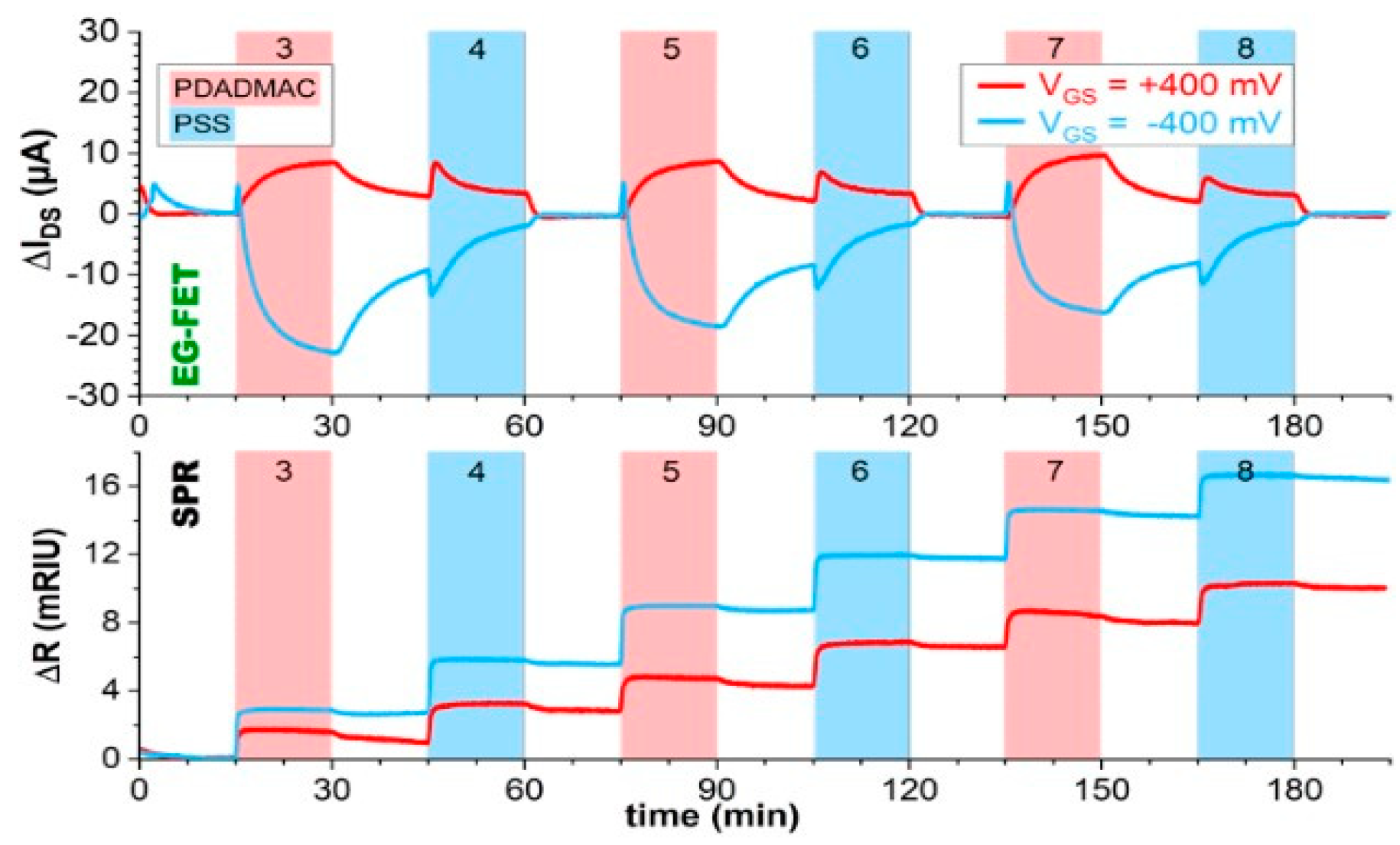
As a test sample, we investigated the build-up of multilayer assemblies, deposited by the layer-by-layer protocol of polyelectrolytes from a solution at the gate electrode/Kretschmann SPR substrate. When monitoring the formation protocol of the multilayer architecture by surface plasmon optics in real time, one can see the monotonous build-up of the assembly with every alternate deposition of a monolayer of the polyanionic poly (diallyl-dimethylammonium chloride) (PDADMAC) and the polycationic poly(styrene-sulfonate) (PSS) (Figure 2). However, by contrast, the electronic signal monitored simultaneously with the graphene channel actually demonstrates that a lot more is happening. And rather significant current changes are not only seen during the deposition but also during the rinsing steps. Up to now, these have never been observed because it was never possible to record them. It can be expected that in other interfacial binding reactions, e.g., during DNA hybridization or for aptamer–ligand interactions, more details than those known at present will become evident.
Other combination modes, e.g., Au gate electrodes modified with nanohole arrays or with grating structures, or the completely new combination of a fiber optic surface plasmon spectrometer with a FET device [2], will be briefly summarized.

Funding

This research received no external funding.

Institutional Review Board Statement

Not applicable.

Informed Consent Statement

Not applicable.

Data Availability Statement

Data sharing is not applicable to this abstract.

Conflicts of Interest

The author declares no conflict of interest.

References

  1. Aspermair, P.; Ramach, U.; Reiner-Rozman, C.; Fossati, S.; Lechner, B.; Moya, S.E.; Azzaroni, O.; Dostalek, J.; Szunerits, S.; Knoll, W.; et al. Dual Monitoring of Surface Reactions in Real Time by Combined Surface-Plasmon Resonance and Field-Effect Transistor Interrogation. J. Am. Chem. Soc. 2020, 142, 11709–11716. [Google Scholar] [CrossRef] [PubMed]
  2. Hasler, R.; Reiner-Rozman, C.; Fossati, S.; Aspermair, P.; Dostalek, J.; Lee, S.; Ibáñez, M.; Bintinger, J.; Knoll, W. Field-Effect Transistor with a Plasmonic Fiber Optic Gate Electrode as a Multivariable Biosensor Device. ACS Sens. 2022, 7, 504–512. [Google Scholar] [CrossRef] [PubMed]
Figure 1. SPR-EGO-FET combination setup for simultaneous surface plasmon optical and electronic monitoring of surface reactions.
Proceedings 97 00196 g001
Figure 2. Electronic (top) and surface plasmon optical (bottom) protocol of the multilayer formation by the layer-by-layer deposition of polyelectrolytes, taken at two different potentials applied to the gate substrate.
Proceedings 97 00196 g002
Disclaimer/Publisher’s Note: The statements, opinions and data contained in all publications are solely those of the individual author(s) and contributor(s) and not of MDPI and/or the editor(s). MDPI and/or the editor(s) disclaim responsibility for any injury to people or property resulting from any ideas, methods, instructions or products referred to in the content.