Proceeding Paper

InAs/GaSb Superlattice Based Mid-Infrared Interband Cascade Photodetectors Grown on Both Native GaSb and Lattice-Mismatched GaAs Substrates

by
Klaudia Hackiewicz
1,*,
Małgorzata Kopytko
1,
Jarosław Rutkowski
1,
Piotr Martyniuk
1 and
Łukasz Ciura
2
1
Institute of Applied Physics, Military University of Technology, 2 Kaliskiego Str., 00–908 Warsaw, Poland
2
Department of Electronics Fundamentals, Rzeszow University of Technology, 2 W. Pola Str., 35959 Rzeszow, Poland
*
Author to whom correspondence should be addressed.
Presented at the 15th International Workshop on Advanced Infrared Technology and Applications (AITA 2019), Florence, Italy, 17–19 September 2019.
Proceedings 2019, 27(1), 38; https://doi.org/10.3390/proceedings2019027038
Published: 9 October 2019

Abstract

:
Electrical and optical properties of interband cascade infrared photodetectors with InAs/GaSb type-II superlattice absorbers are investigated in this work. We compare the detection parameters of detectors grown on the native GaSb substrate and lattice-mismatched GaAs substrate and seek solutions to enhance device performance, specifically with using an optical immersion. The detectors grown on GaAs have better detection parameters at room temperature, but at lower temperatures the misfit dislocations become more important and detectors grown on GaSb become better.

1. Introduction

Due to the stronger, less ionic chemical bond, III-V semiconductors are more robust and stable than their II-VI equivalent. Considerable progress towards III-V materials technology has been made, especially for low-dimensional solids such as type-II superlattices (T2SLs). The growth of T2SLs can be carried out with better control over the structure and greater reproducibility. The ability to independently adjust the positions of the conduction and valence band edges in T2SLs and other III-V materials is one important advantage that gives the opportunity to design new detector architectures. Especially emerging as a viable alternative for high performance, high-operation temperature (HOT) infrared detectors are interband cascade infrared photodetectors (ICIPs) [1], particularly for temperatures above a room temperature, even up to 400 K.
The basic concept of operation of ICIPs is a multiple-stage design with a thin T2SL absorber. The absorber in each stage is sandwiched between coupled multiple-quantum wells (M-QWs) tunneling region, which is also an electron blocking barrier and coupled multiple M-QWs relaxation region (hole blocking barrier). These multiple-stages are electrically connected in series. An enhanced electron barrier design could drastically suppress the device dark current, particularly at higher reverse biases. Our previous work [2] shows that the dark current in ICIPs is ultimately limited by the generation current originating from Shockley-Read-Hall (SRH) and Auger processes.
In this paper, we present investigations of electrical and optical properties of mid-wave infrared (MWIR) ICIPs based on InAs/GaSb T2SLs absorbers and seek solutions to enhance device performances, specifically with using an optical immersion. T2SLs based ICIPs are demonstrated both on native GaSb and lattice-mismatched GaAs substrates. So far, devices grown on GaAs substrates have slightly lower parameters than their lattice-matched equivalents [3,4]. The choice of GaAs substrate was dictated by the possibility of hyperhemispherical immersion lens formation. In addition, growth on GaAs also offers lower cost and larger area substrates.

2. Devices Design

Samples were grown by a Veeco Gen-10 solid-source molecular beam epitaxy (MBE) system both on native GaSb substrate and lattice-mismatched GaAs substrate with GaSb buffer layer deposited with the interfacial misfit (IMF) array growth mode. IMF growth mode gives minimum possible threading dislocations. Both devices consist of a GaSb bottom contact layer. For the sample grown on native GaSb, bottom contact is 300 nm thick and is n-type doped with tellurium to a level of 2 × 1018 cm−3. For the sample grown on lattice-mismatched GaAs, IMF grown bottom contact is 2.5 μm thick and is p-type doped with beryllium to a level of 2 × 1018 cm−3. This is the only difference in the architecture of both detectors. Bottom contact is followed by five cascade stages. Each stage consists of a 47 nm thick InAs/AlSb M-QWs hole barrier, InAs/GaSb SL absorber and a 48 nm thick AlSb/GaSb M-QWs electron barrier. The absorber region is made of a non-intentionally-doped 7-ML InAs/8-ML GaSb T2SL (ML stands for mono-layer), with a thickness of 30 periods in each stage, which gives the total thickness of 146 nm. The residual doping in the MWIR T2SL at high temperatures has been reported to be n-type [5]. Barrier layers are non-intentionally-doped as well. Cascades are followed by a 15 nm thick top contact layer, made of n-type InAs doped with tellurium to a level of 2 × 1018 cm−3.

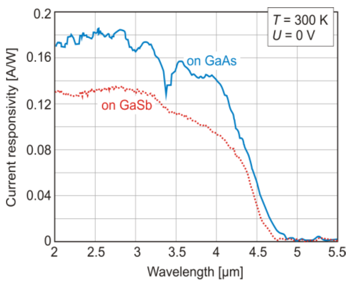
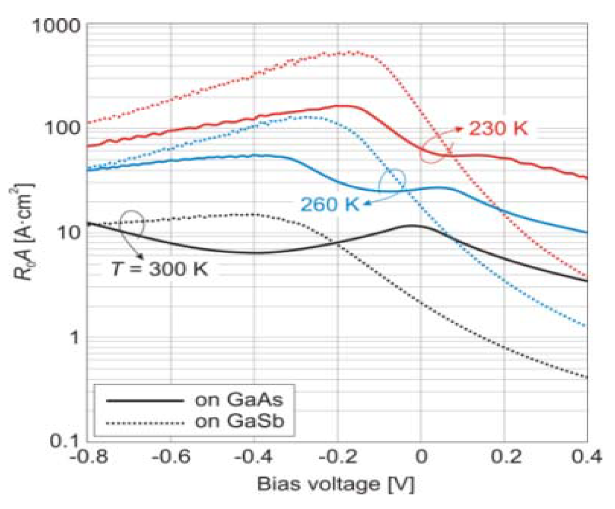
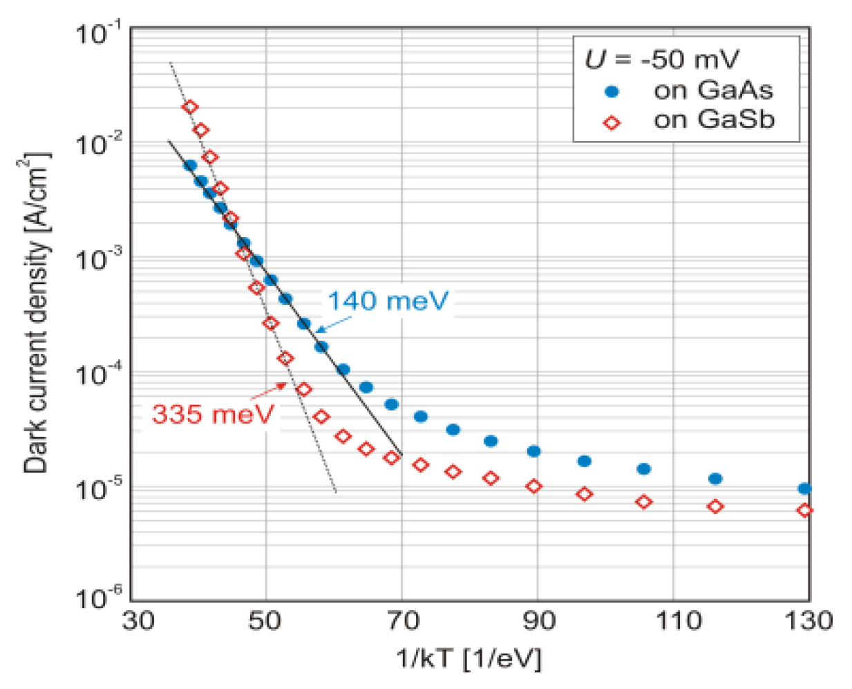
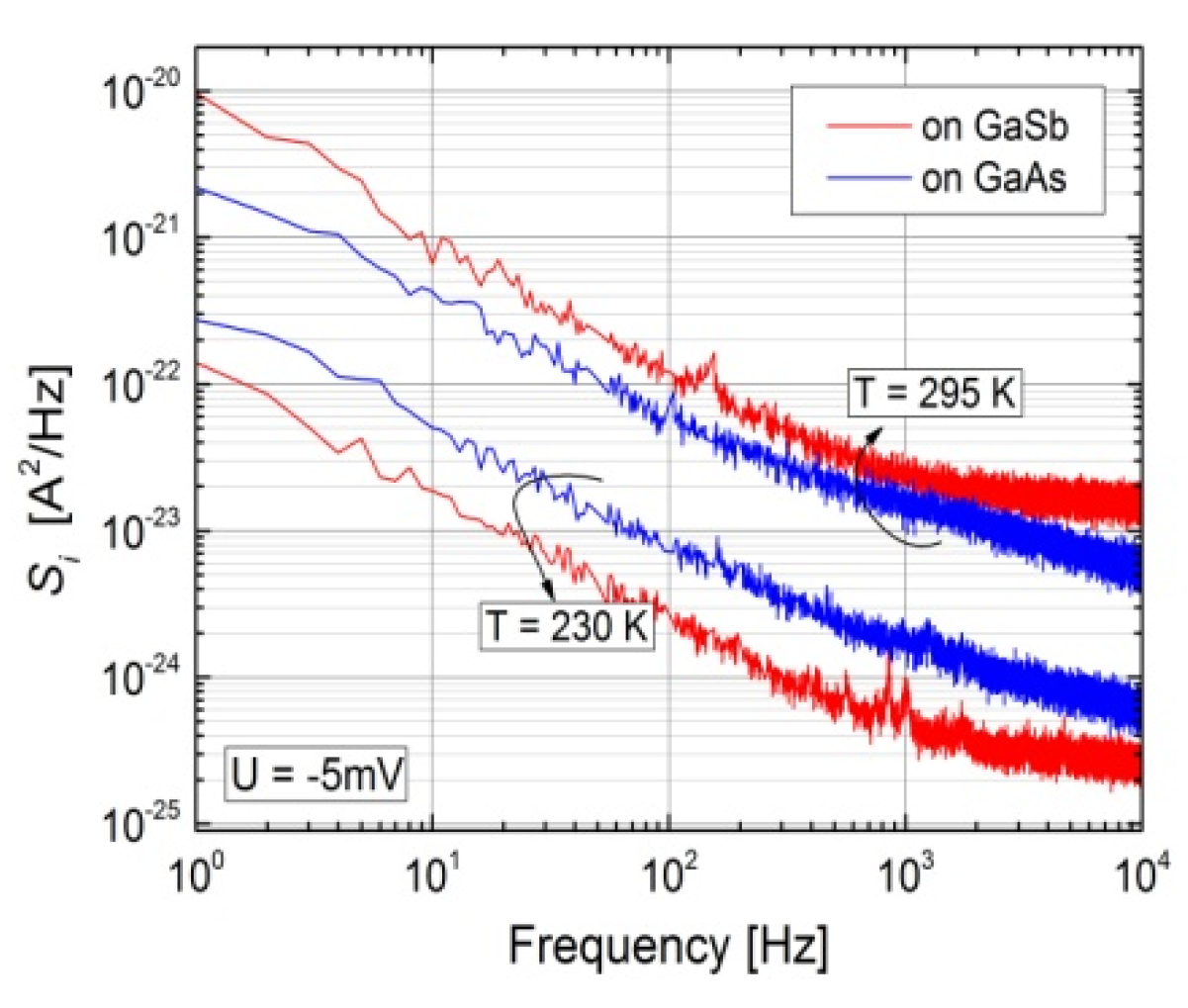
3. Results and Discussion

The spectral characteristics have been measured at zero bias and 300 K. As shown in Figure 1, 50% cut-off wavelengths (λcut-off) are around 4.3 μm at 300 K for both devices. Slight shift of the λcut-off value may be associated with higher strains in the sample grown on GaAs. Current responsivities are not so high, up to 0.18 A/W and 0.14 A/W for the sample grown on GaAs and GaSb, respectively.
Electrical measurements in dark conditions at different operating temperatures were performed. At 230 K, the sample grown on lattice-mismatched GaAs shows the highest values ​​of the dark current in a whole range of a negative bias. The point at which product of dynamic resistance and detector area (RdA) of both devices are equal moves towards higher voltages as the temperature increases (Figure 2). What is more, the detector grown on GaAs substrate shows a specific behavior of dynamic resistance as a function of voltage, with two maximum values. It is of particular interest to achieve extreme values at around zero bias voltage. At high temperatures, R0A product is much higher for the detector on GaAs. Together with a higher current responsivity, this will translate into a higher detectivity D*.
It would be expected that due to the misfit dislocation, the detector grown on GaAs will show worse performance. The activation energy Ea can be determined by a fitting to the relation:
J D A R K ~ T s e x p ( E a k T ) ,
where k is the Boltzmann constant and T is the temperature. The power s is equal to 1.5. Arrhenius plots of the dark current density at a bias of −50 mV are shown in Figure 3. For the sample grown on native GaSb, the high-temperature activation energy of 335 meV is related to the absorber layer bandgap at 0 K indicating diffusion behavior.
Over the past decade, a lot of attention has been paid to the differential resistance and quantum efficiency of T2SL devices and most groups focused on improving these two critical parameters, assuming that thermal (Johnson) or/and shot noise limit the sensitivity of the detector. In contrast, there are many noise sources in infrared detector, some of which depend on the frequency f. Therefore, the detector noise taken into account in the D* should be calculated in accordance with:
i n ( f ) = 4 k T / R + 2 q I + S i ( 1   Hz ) / f ,
where Si(1 Hz) is power spectral density of current noise at 1 Hz. Infrared detectors operating with bias may suffer from 1/f noise in the low frequency range. Then, their low frequency detectivity is no longer determined by thermal or shot noise but by the 1/f noise, as shown in the Figure 4. For this reason, low frequency noise measurements of the ICIPs are also presented in this paper.
If detector operates under zero bias and assuming that the normalized detectivity is limited only by Johnson noise, the D*can be assessed according to the relation:
D * = R i / 4 k T / R 0 A ,
where Ri is the current responsivity. Table 1 compares the normalized D* of both detectors, calculated for 300 K and a zero bias voltage, according to the Equation (3). Values of Ri were taken at 4 μm. The D* of both detectors is at the same order of magnitude. However, due to higher values of the Ri and R0A product, the detector grown on GaAs achieves 3 times higher value of the D*, at the level of 3.5 × 10⁹ cmHz1/2W−1.
The detectivity improvement might be obtained by the increase of the apparent optical size of the detector in comparison with its actual physical size by using a suitable optical concentrator. However, practical use of immersion technology might by limited due to problems with matching of the detector and lens materials. It has been solved by the use of monolithic technology developed at VIGO System S.A. [6]. Hyperhemispherical immersion lens is formed from GaAs substrates by using numerically controlled micromachining [7]. An alternative approach for GaSb substrate is the use of micromachining technique involving dry etching to fabricate immersion lens integrated with the device [8]. This formation gives a hemispherical lens shape rather than a hyperhemispherical.
Table 1 also lists values of the D* that can be obtained using optical immersion. We have assumed the use of a hyperhemispherical lens for a GaAs substrate and a hemispherical lens for a GaSb one. The detectivity gain achieved with hyperhemispherical immersion is substantially higher compared to those for hemispherical immersion and amounts n2 and n, respectively, where n is the refractive index of the substrate. The values of refractive indices were assumed on the basis of Adachi model [9] and amount to 3.3 and 3.7 for GaAs and GaSb, respectively. The normalized detectivity of the detector grown on GaAs is of about an order of magnitude higher than for the detector grown on GaSb.

4. Conclusions

We have compared the detection parameters of the interband cascade infrared photodetectors (ICIPs) with InAs/GaSb type-II superlattices absorbers grown on the native GaSb substrate and lattice-mismatched GaAs substrate. Proper superlattice quality was obtained either on GaSb or GaSb-buffered GaAs substrates growth using the interfacial misfit array growth mode technique. The substrate has a strong impact, which is related to the misfit dislocation and quality of the examined superlattices. The ICIPs grown on lattice-mismatched GaAs substrate have better current responsivity, R0A product, lower noise and higher detectivity at room temperature. However, at lower temperatures the misfit dislocations become more important and those detection parameters deteriorate in comparison with the detection parameters of ICIP with GaSb substrate. What is more, the use of GaAs substrate makes it possible to create a hyperhemispherical immersion lens that significantly increases the normalized detectivity D*. Even if a lens integrated with a GaSb-grown detector is used, their D* is about the order of magnitude lower.

Acknowledgments

This paper has been done under financial support of the project GBMON/13-995/2018/WAT and TECHMATSTRATEG1/347751/5/NCBR/2017.

Conflicts of Interest

The authors declare no conflict of interest.

References

  1. Li, J.V.; Yang, R.Q.; Hill, C.J.; Chuang, S. L. Interband cascade detectors with room temperature photovoltaic operation. Appl. Phys. Lett. 2005, 86, 1–3. [Google Scholar] [CrossRef]
  2. Hackiewicz, K.; Martyniuk, P. Type-II InAs/GaSb (InAsSb) superlattices for interband cascade midwavelength detectors. Opt. Eng. 2018, 57, 1–5. [Google Scholar] [CrossRef]
  3. Steenbergen, E.H.; Nunna, K.; Ouyang, L.; Ullrich, B.; Huffaker, D.L.; Smith, D.J.; Zhang, Y.-H. Strain-balanced InAs/InAs1−xSbx type-II superlattices grown by molecular beam epitaxy on GaSb substrates. J. Vac. Sci. Technol. B 2012, 30, 02B107. [Google Scholar] [CrossRef]
  4. Plis, E.; Rodriguez, J.B.; Balakrishnan, G.; Sharma, Y.D.; Kim, H.S.; Rotter, T.; Krishna, S. Mid-infrared InAs/GaSb strained layer superlattice detectors with nBn design grown on a GaAs substrate. Semicond. Sci. Technol. 2010, 25, 1–4. [Google Scholar] [CrossRef]
  5. Gautam, N.; Myers, S.; Barve, A.V.; Klein, B.; Smith, E.P.; Rhiger, D.R.; Dawson, L.R; Krishna, S. High operating temperature interband cascade midwave infrared detector based on type-II InAs/GaSb strained layer superlattice. Appl. Phys. Lett. 2012, 10, 3–7. [Google Scholar] [CrossRef]
  6. Kaniewski, J.; Orman, Z.; Piotrowski, J.; Sioma, M.; Ornoch, L.; Romanis, M. Epitaxial InAs detectors optically immersed to GaAs microlenses. Proc. SPIE 2003, 4369, 721–729. [Google Scholar]
  7. Martyniuk, P.; Benyahia, D.; Kowalewski, A.; Kubiszyn, Ł.; Stępień, D.; Gawron, W.; Rogalski, A. Mid-wave T2SLs InAs/GaSb single pixel PIN detector with GaAs immersion lens for HOT condition. Solid-State Electron. 2016, 119, 1–4. [Google Scholar] [CrossRef]
  8. Soibel, A.; Keo, S.A.; Fisher, A.; Hill, C.J.; Luong, E.; Ting, D.Z.; Gunapala, S.D.; Lubyshev, D.; Qiu, Y.; Fastenau, J.M.; et al. High operating temperature nBn detector with monolithically integrated microlens. Appl. Phys. Lett. 2018, 112, 041105. [Google Scholar] [CrossRef]
  9. Adachi, S. Optical dispersion relations for GaP, GaAs, GaSb, InP, InAs, InSb, AlxGa1-xAs, and In1-xGaxAsyP1-y. J. Appl. Phys. 1989, 66, 6030–6040. [Google Scholar] [CrossRef]
Figure 1. Spectral photoresponse for T2SLs based ICIPs grown on GaSb and GaAs substrates.
Proceedings 27 00038 g001
Figure 2. R0A product characteristics versus bias for T2SLs based ICIPs grown on GaSb and GaAs substrates.
Proceedings 27 00038 g002
Figure 3. Arrhenius plots of the dark current density at -50 mV for T2SLs based ICIPs grown on GaSb and GaAs substrates.
Proceedings 27 00038 g003
Figure 4. Power spectral density of current noise Si versus frequency, measured at bias voltage -5 mV for T2SLs based ICIPs grown on GaSb and GaAs substrates.
Proceedings 27 00038 g004
Table 1. The D* of T2SLs based ICIPs operated at 300 K. Values of Ri were taken at 4 μm.
Detector TypeRi (0 V)
[AW−1]
R0A
[Ωcm2]
D*
[cmHz1/2W−1]
Non-Immersed
D*
[cmHz1/2W−1]
Optically Immersed
T2SLs IC on GaAs0.14103.5 × 1093.7 × 1010
T2SLs IC on GaSb0.0921 × 1093.7 × 109

