1. Introduction
The strain gauge tests of printed circuit boards (PCB) represents complex work including FEA analysis, strain gauges installation and measurement and sometimes metallographic analysis of the cracked soldered joint, which often is the initiation for the own strain investigation.
Strain based printed circuit board (PCB) flexure control allows objective analysis of strain and strain rate levels during all PCB manufacturing steps, e.g., assembly, tests and any other types of operation including usage of the manufactured device. This method can improve manufacturing operations, that can pose high risk for interconnect damage. Excessive strains can result in solder ball cracking, trace damage, pad lifting and package substrate cracking. The guidelines for these tests are described in JEDEC methodology [
1]. Although this standard is focused mainly to surface mount devices, the test approach can be used also for non-area-discrete SMT devices. The strain limits however are specified in non-obligatory IPC-WP-01 white paper only and have to be stated always by customer.
Typically, two test boards are instrumented, one after reflow with SMT components only, the other after wave solder with both SMT and trough-hole components. Appropriate wire management, bundling and securing the wires is important. The wires should be run between components, where they will not interfere with any process steps.
The article should contribute to this work in the area of measurements and evaluations of strains during PCB assembly and splitting.
2. Material and Methods
The main objective of PCB tests is to determine the principal strains in the areas of high strain concentration especially at the corners of large circuit components [
2]. The strain gauge rosettes with the grid length smaller than 1 mm are used for this purpose. We use the strain gauge rosettes TML FRA–1-11–3L with integrated cables. For some components the strain gauge with only one grid are sufficient. We use the Vishay strain gauges type EA-06-031DE or HBM LY11/0.6 [
3].
High strains can destroy the solder joint not only during the PCB assembly but also during the PCB operation in the apparatus (especially in the vehicles).
According the JEDEC Methodology, the sample frequency during the strain measurement should be in the interval between 500 Hz and 2000 Hz. We use the frequency 1600 or 800 Hz. The main problem for PCB strain measurement is to use the proper measurement unit with sufficient number of channels. For the test with 10 strain gauge rosettes the number of minimum channels is 30. We use special measurement unit, made from Czech firm Pohl—EMS DV803, which enables the measurement at 3200 Hz for 32 channels. It is possible to combine four measuring units together and thus performed measurement up to 128 channels at the same time. However, the strain time histories should be filtered with LP filter to remove disturbing peaks but keeping the real structure strain peaks.
3. Results
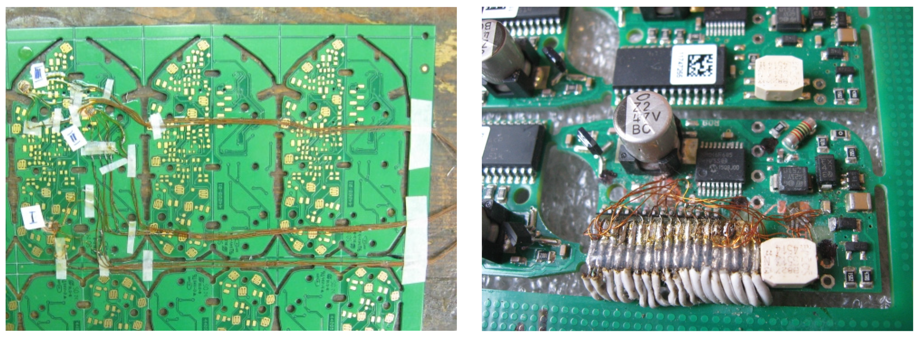
3.1. Cables Wiring
Often the tests are performed on multi panels, containing several PCBs, which are separated by cutting or milling in the end of their assembly. The proper installation of wires is important especially in these cases. The wires should be run between components, where they will not interfere with any process steps. An example of doing this is given in
Figure 1. Here the terminal board is formed on the upper side of one IC, because the wires have to be led on upper or bottom part of the PCB depending on tested assembly step. The use of enameled wires instead of thick standard insulation has approved on the board. Outside the board the cables with standard insulation are used.
3.2. Test Results
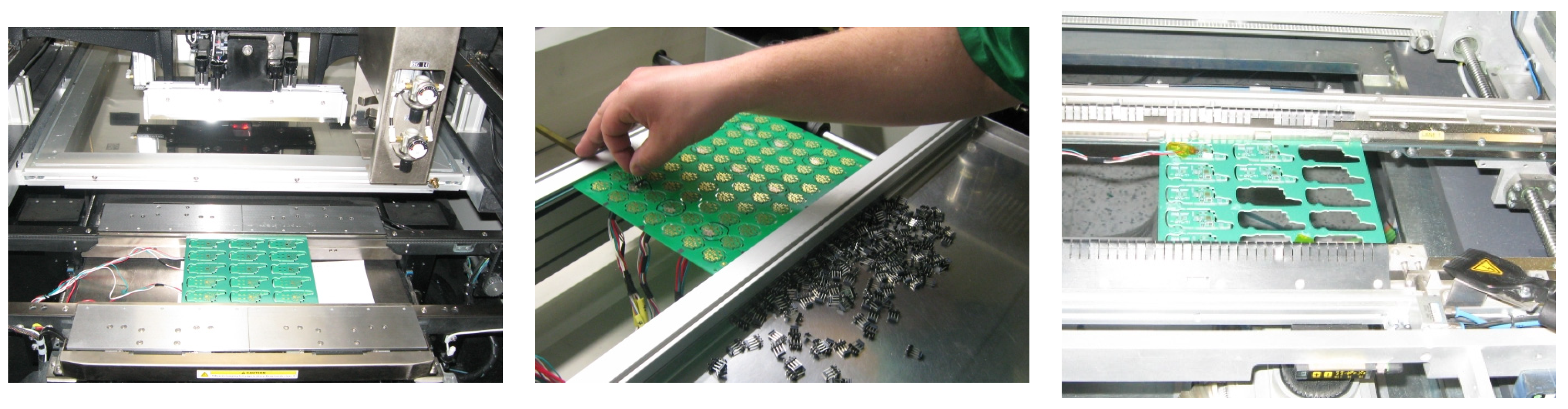
An example of some operations with instrumented PCB is given in
Figure 2. Some procedures are only simulated without heating but with presence of loads to avoid strain gauge destruction (e.g., solder paste printing). Tests are performed on several machines in the assembly line.
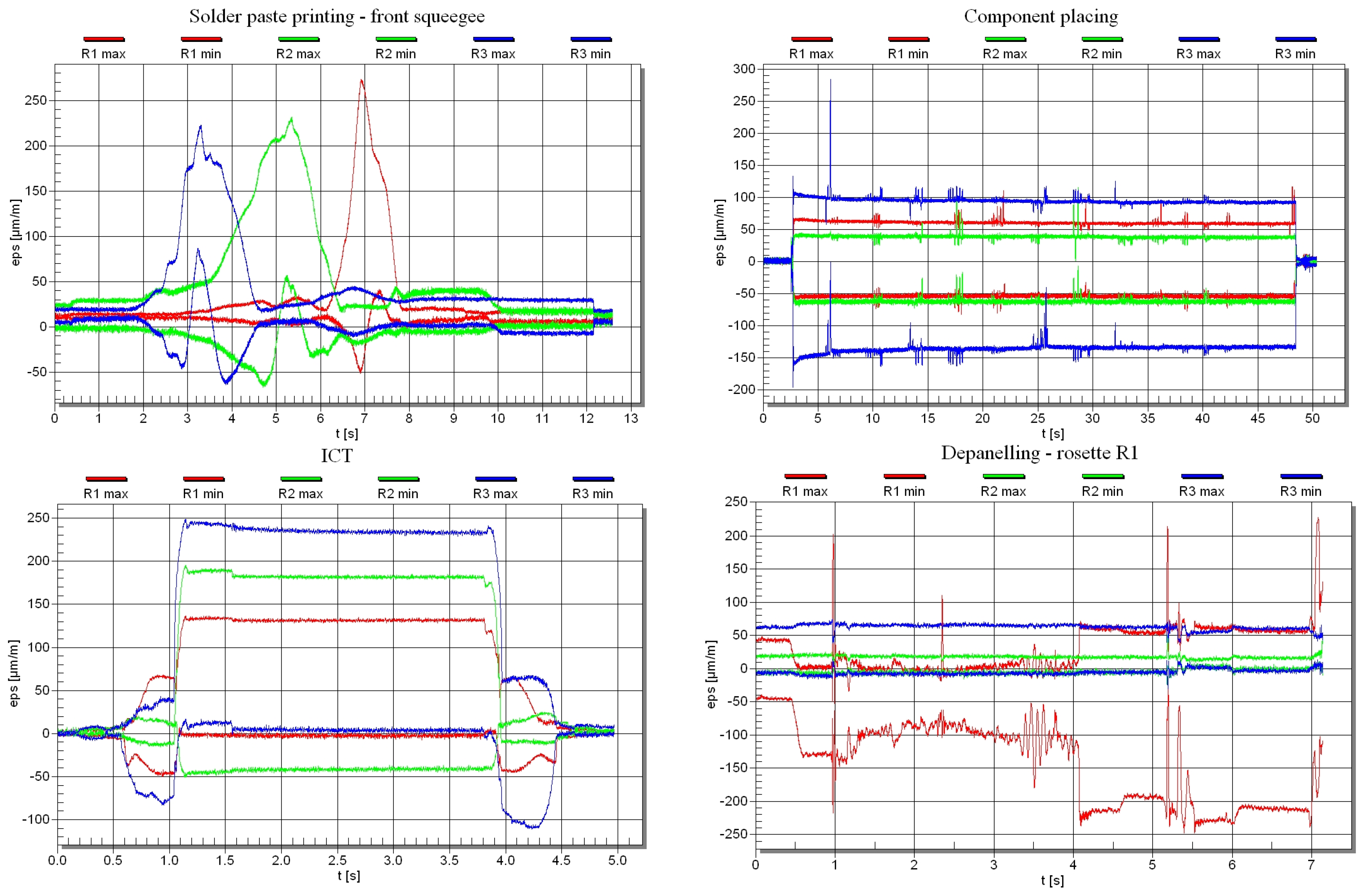
Different strain time histories at different strain levels and rates are measured during different manufacturing steps. Strain histories of solder paste printing, inspection (IOD), components deposition and PCB cutting (depanelling from the multi-panel) are shown in
Figure 3. Here evaluated main principal strains are presented.
Another task is strain optimization during the assembly of the finished PCB to its case. The detail of strain—time history during assembly of the PCB to the case of some control unit is given in
Figure 4. Here, the evaluated maximum principle strain and shear strain and their rates are given.
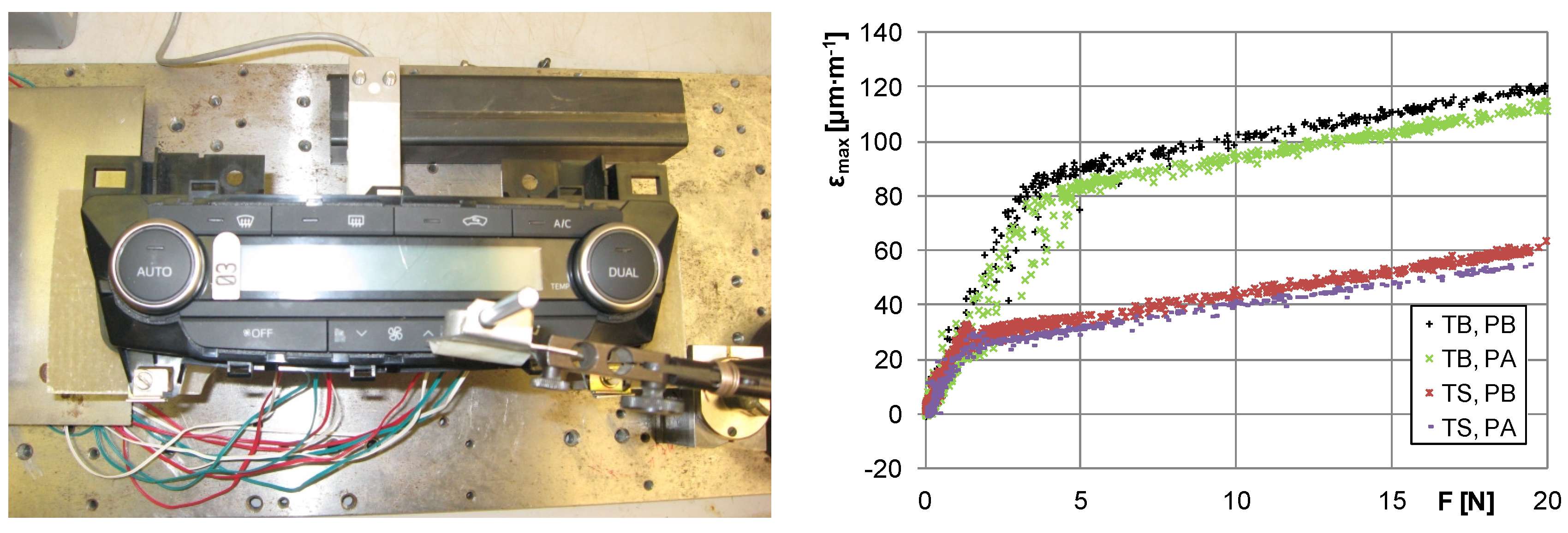
Some tests are performed during operation of the assembled device. The strain response vs. applied force of pushing one button of the car air-condition control box is given in
Figure 5. The goal was to lower the strain either by lowering the backstops of the box (from PB to PA) or by adding the button backstops (TB to TS). The whole box was placed on single-point type of load cell and the force was induced statically with the screw as well as dynamically with the finger.
It has been approved, that the box design has not significant influence to strain level (both narrow chart relations). The button stops results strain drop to more than 50% without loss of the button functionality.
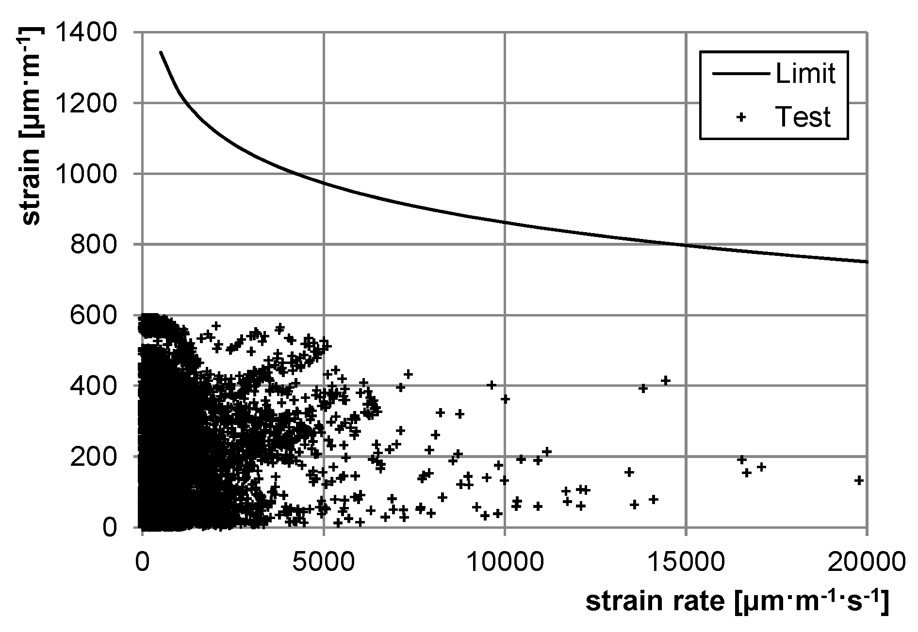
The allowable strain is the function of PCB thickness and also the stress rate. In
Figure 6, the distribution of all measured strains is related to allowable value inclusive the strain rate (the allowable strain lowers with increasing rate).
4. Conclusions
The strain gauge tests of printed circuit boards represents complex work including FEA analysis, strain gauges installation and measurement and sometimes metallographic analysis of the cracked soldered joint, which often is the initiation for the own strain investigation. The article should contribute to this work.
