Proceeding Paper

Displacement Sensor with Inherent Read-Out Circuit Using Water-Gated Field Effect Transistor (WG-FET) †

Dept. of Electrical & Electronics Eng., Bogazici University, 34342 Istanbul, Turkey
*
Author to whom correspondence should be addressed.
Presented at the Eurosensors 2018 Conference, Graz, Austria, 9–12 September 2018.
Proceedings 2018, 2(13), 926; https://doi.org/10.3390/proceedings2130926
Published: 26 November 2018
(This article belongs to the Proceedings of EUROSENSORS 2018)

Abstract

:
This paper presents, for the first time, a displacement sensor with inherent read-out circuit using an inverter built with WG-FET that has 16-nm-thick single crystalline silicon film. In WG-FET, electrical double layer (EDL) capacitances are formed at water/silicon and water/top gate interfaces. These two capacitances and the resistance of the de-ionized (DI) water droplet build a first order RC network. Propagation delay of an inverter built with WG-FET depends on this RC constant. When the distance between top gate and silicon film changes, EDL capacitances remain the same, but resistance of the DI-water droplet changes. Accordingly, propagation delay of the inverter changes linearly with this distance. Increasing the distance from 400 µm to 1200 µm changes low-to-high propagation delay tplh of the inverter from 1.08 ms to 1.36 ms and high-to-low propagation delay tphl from 0.48 ms to 0.56 ms, which yields sensitivities of 0.35 µs/µm and 0.1 µs/µm, respectively.

1. Introduction

Water-gated field effect transistors (WG-FET) that use 16-nm-thick single crystalline silicon film as active layer have a high potential in chemical and biological sensors because of their liquid-solid interfaces and capability to form integrated read-out circuit [1,2,3,4]. In WG-FET, EDL capacitance at water/silicon interface is used as gate insulator, which allows easy and low-cost fabrication of a low voltage device with high channel control. In addition, EDL capacitances on both interfaces are independent of the distance between top gate and silicon layer, which simplifies the read-out process. Dependence of the DI-water resistance on the distance between top gate and silicon film makes the RC time constant of the inverter built with WG-FET sensitive to displacements. Since capacitances remain the same while only the resistance changes, the sensor response becomes approximately linear.
A strain sensor [5] and a tactile sensor [6] have been shown before to give information about change in displacement by measuring resistance of liquid passively. However, since passive liquid resistance measurements involve EDL capacitances on electrodes and parasitic capacitances of wires and connectors, sensitive measurements become challenging. On-site active measurement with integrated read-out circuit can buffer and amplify electrical signal, solving problems of noise and parasitics. In this work, an active displacement sensor with inherent read-out circuit is demonstrated using a WG-FET for the first time. The WG-FET with 16-nm-thick silicon film as shown in Figure 1 is used to build a digital inverter gate.

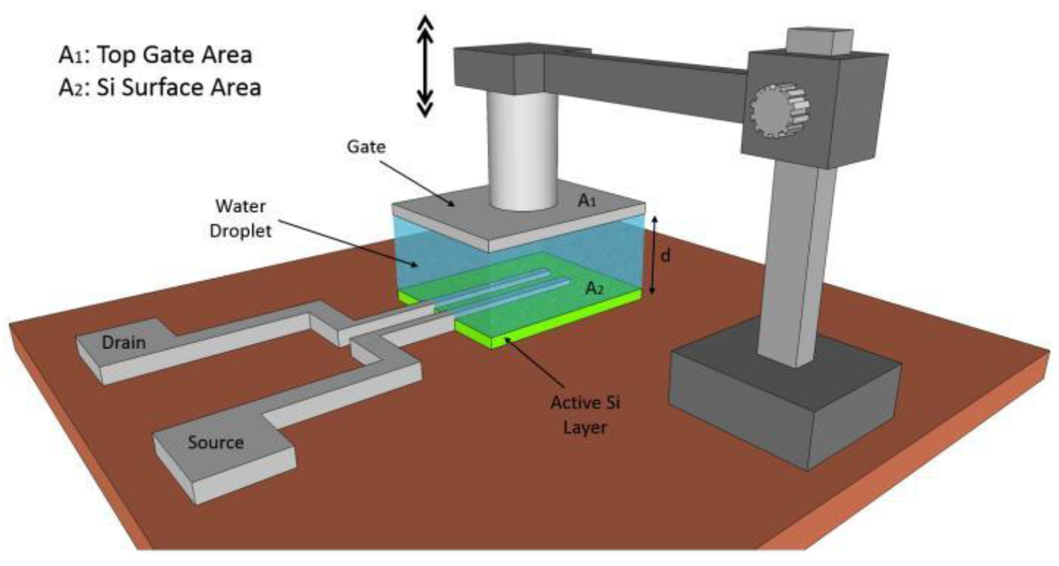
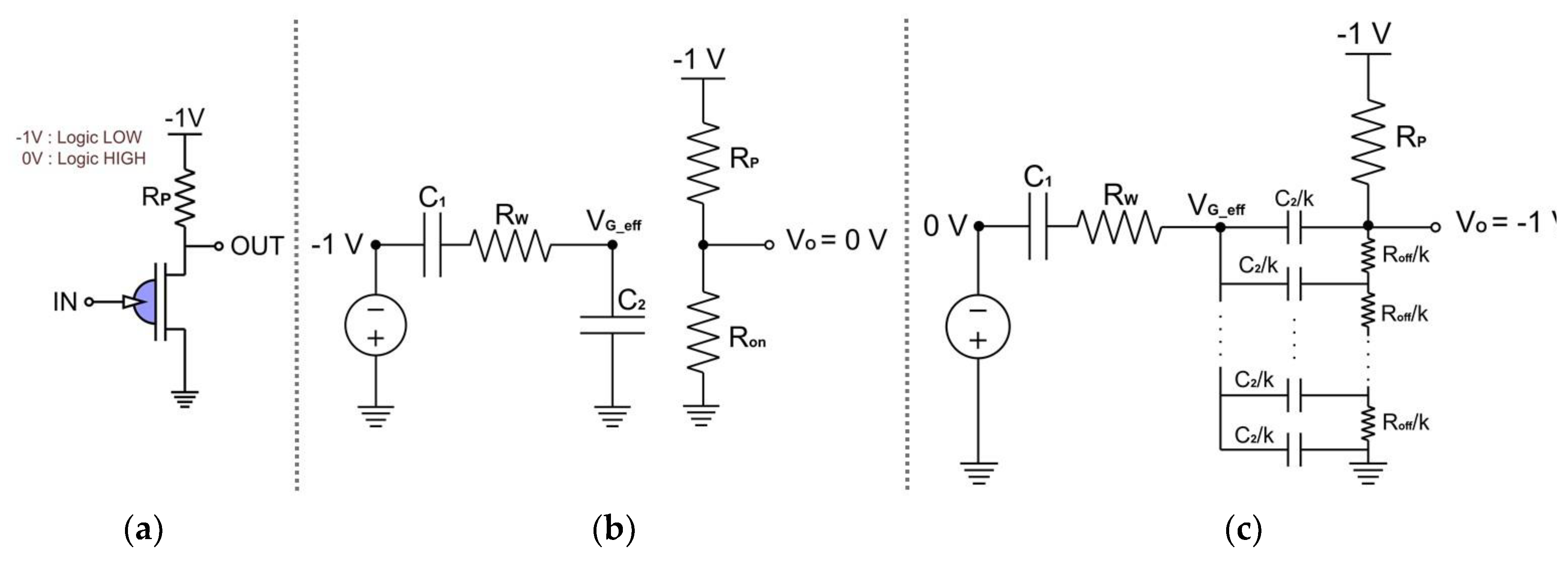
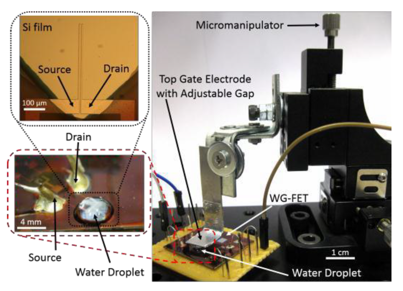
2. Materials and Methods

The fabrication steps of the WG-FET were reported before [4]. The inverter configuration using a WG-FET and a pull-down resistor is given in Figure 2a. In this WG-FET, DI-water droplet resistance and EDL capacitances on silicon and top gate surfaces compose an RC network. The equation of the resistance is given as
R w = ρ d A
where Rw is the resistance of the DI-water droplet, is the resistivity of DI-water, d is the distance between Si layer and top gate and A is the area of the active Si layer and top gate surface. Simplified equations of the EDL capacitances can be given as
C = C 1 = C 2 = ε A λ
where C1 is the EDL capacitance on top gate surface, C2 is the EDL capacitance on Si layer surface, ε is the permittivity of DI-water and λ is the double layer thickness.
When WG-FET is turned on, the voltage across its source and drain becomes approximately zero. This condition leads to the equivalent circuit shown in Figure 2b. In this equivalent circuit, equation of the low-to-high propagation delay, tplh, can be expressed as
t p l h R w C 2 ρ ε d 2 λ
However, when WG-FET is turned off, a voltage drop close to the voltage level supplied by power supply appears across its active channel. Therefore, its off-resistance Roff and gate capacitance C2 must be modeled as a distributed network as shown in Figure 2c. The equivalent capacitance C2eq in this distributed network can be approximated as
C 2 e q C 6
which gives the equation of the high-to-low propagation delay as
t p h l R w C 7 ρ ε d 7 λ
Since resistivity and permittivity of DI-water and double layer thickness are constant, propagation delays change linearly with displacement, d.
WG-FET with top gate electrode and adjustable gap is prepared with the help of a micromanipulator as shown in Figure 3. An aluminum plate is shaped as parallel plate and connected to the micromanipulator. DI-water droplet is placed between the silicon surface and this plate. An inverter circuit is built by connecting an external pull-down resistor to this device. This way, a linear displacement sensor with inherent read-out circuit is formed.

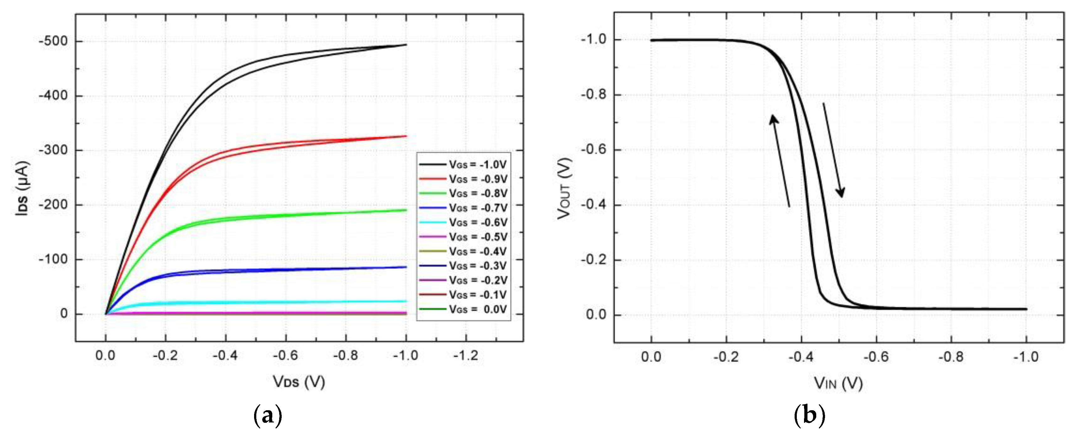
3. Results and Discussion

Characteristic IDS-VDS curves of the WG-FET are presented in Figure 4a, which show the typical characteristics of the WG-FET. A maximum current of 500 µA and an on-off ratio of 86,000 A/A are obtained, where the maximum applied voltage is kept at 1 V. This transistor is used in the inverter configuration. Voltage transfer curve (VTC) of the inverter is shown in Figure 4b, which displays a rail-to-rail response with a typical gain of 6.7 V/V.
For characterization of the displacement sensor, a square wave with 100 Hz frequency and 1 V peak-to-peak voltage is applied as input. Output voltages are observed for different distances. As an example, input and output voltage-time graphs are given for 1000 µm distance between silicon layer and top gate electrode in Figure 5a, which also shows the propagation delays. For each distance, propagation delays tplh and tphl are extracted from the voltage-time curves and plotted in Figure 6b with their linear approximations. When the distance between top gate and silicon layer is increased from 400 µm to 1200 µm, low-to-high propagation delay tplh of the inverter increases from 1.08 ms to 1.36 ms, yielding a sensitivity of 0.35 µs/µm; whereas high-to-low propagation delay tphl increases from 0.48 ms to 0.56 ms, resulting a sensitivity of 0.1 µs/µm.
These results agree with the theoretical assumption that propagation delays change linearly with the distance. Also, as proposed by the Equations (3) and (5), low-to-high propagation delay is 3.5. times higher than high-to-low propagation delay.

4. Conclusions

It is concluded that changing the distance between top gate and silicon layer of a WG-FET changes the RC time constant linearly since this changes the resistance of the DI-water while keeping the EDL capacitances on both surfaces constant. Therefore, an active displacement sensor with inherent read-out circuit can be realized using WG-FETs. This can be in the form of a digital inverter gate measuring propagation delay as in this work. Similarly, WG-FETs can be used in analog circuit configurations such as common-source or differential amplifiers to measure displacement.

Author Contributions

S.M. conceived and designed the experiments; O.E. and B.G.S. performed the experiments; O.E., B.G.S. and S.M. analyzed the data; O.E. wrote the paper.

Acknowledgments

This work is supported by Scientific and Technological Research Council of Turkey (TUBITAK) under project EEEAG 114R080.

Conflicts of Interest

The authors declare no conflict of interest.

References

  1. Ertop, O.; Sonmez, B.G.; Mutlu, S. Realization of planar water-gated field effect transistor (WG-FET) using 16-nm-thick single crystalline Si film. Procedia Eng. 2014, 87, 76–79. [Google Scholar] [CrossRef]
  2. Sonmez, B.G.; Ertop, O.; Mutlu, S. Improved repeatability in planar water-gated field effect transistor (WG-FET) with 16-nm-thick single crystalline Si film. Procedia Eng. 2016, 168, 1739–1742. [Google Scholar] [CrossRef]
  3. Ertop, O.; Sonmez, B.G.; Mutlu, S. Investigation of the salt concentration dependence of water-gated field effect transistors (WG-FET) using 16-nm-thick single crystalline Si film. Proceedings 2017, 1, 486. [Google Scholar] [CrossRef]
  4. Sonmez, B.G.; Ertop, O.; Mutlu, S. Modelling and realization of a water-gated field effect transistor (WG-FET) using 16-nm-thick mono-Si film. Sci. Rep. 2017, 7, 12190. [Google Scholar] [CrossRef] [PubMed]
  5. Chossat, J.; Park, Y.; Wood, R.J.; Duchaine, V. A soft strain sensor based on ionic and metal liquids. IEEE Sens. J. 2013, 13, 3405–3414. [Google Scholar] [CrossRef]
  6. Yeo, C.Y.; Yu, J.; Shang, M.; Loh, K.P.; Lim, C.T. Highly Flexible Graphene Oxide Nanosuspension Liquid-Based Microfluidic Tactile Sensor. Small 2016, 12, 1593–1604. [Google Scholar] [CrossRef]
Figure 1. WG-FET with adjustable top gate electrode gap.
Proceedings 02 00926 g001
Figure 2. (a) Inverter circuit; (b) Inverter equivalent circuit when WG-FET is on; (c) Inverter equivalent circuit when WG-FET is off.
Proceedings 02 00926 g002
Figure 3. WG-FET under test with a parallel plate top gate electrode with adjustable gap.
Proceedings 02 00926 g003
Figure 4. (a) IDS vs. VDS curves of WG-FET; (b) Voltage transfer curve of inverter.
Proceedings 02 00926 g004
Figure 5. (a) VIN and VOUT vs. time curves of inverter for 1000 µm distance; (b) tphl and tplh vs. distance curves and their linear approximations.
Proceedings 02 00926 g005
Publisher’s Note: MDPI stays neutral with regard to jurisdictional claims in published maps and institutional affiliations.

