SPAD-Based LiDAR Sensor in 0.35 µm Automotive CMOS with Variable Background Light Rejection †

 ,
, 
Abstract
:1. Introduction
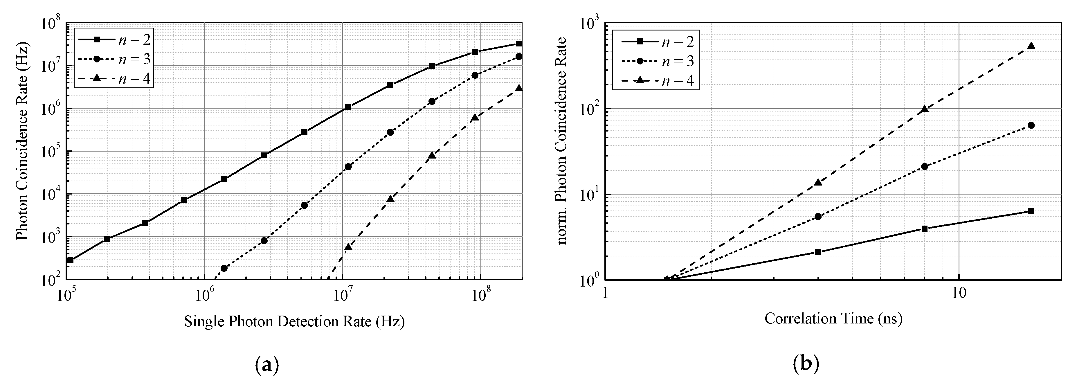
2. Photon Coincidence
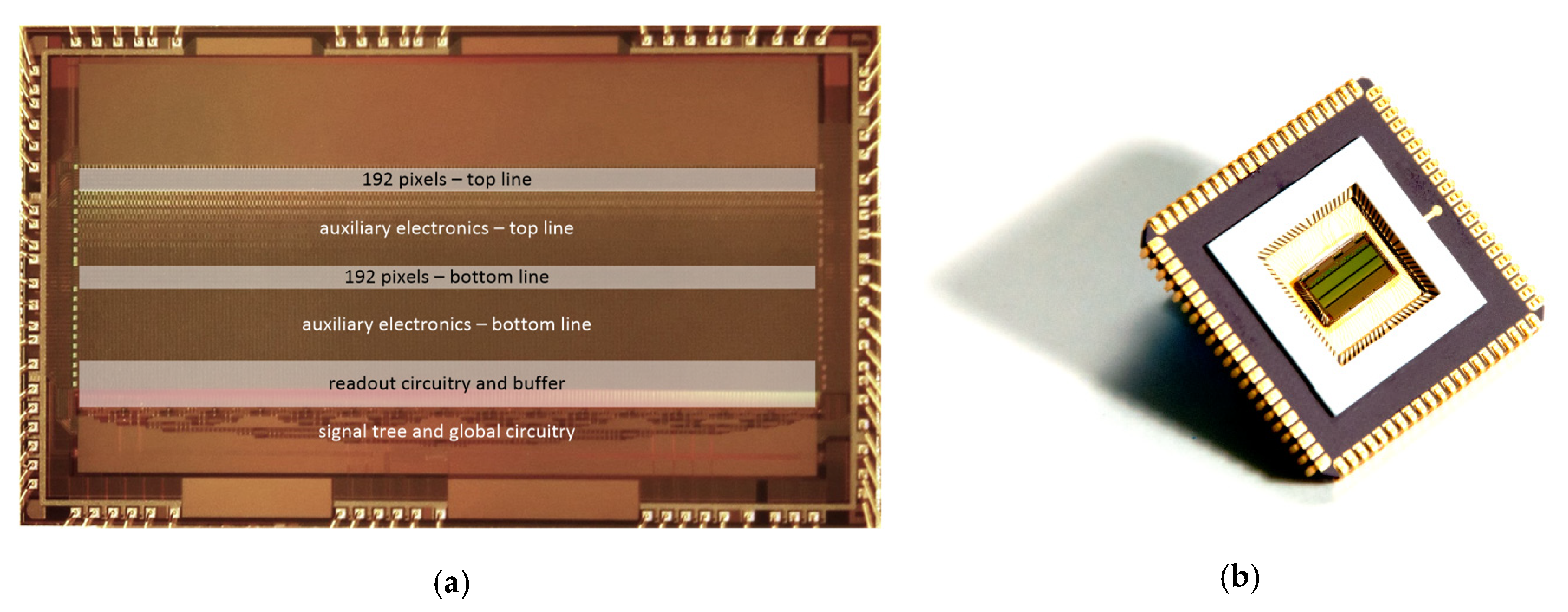
3. Sensor Design
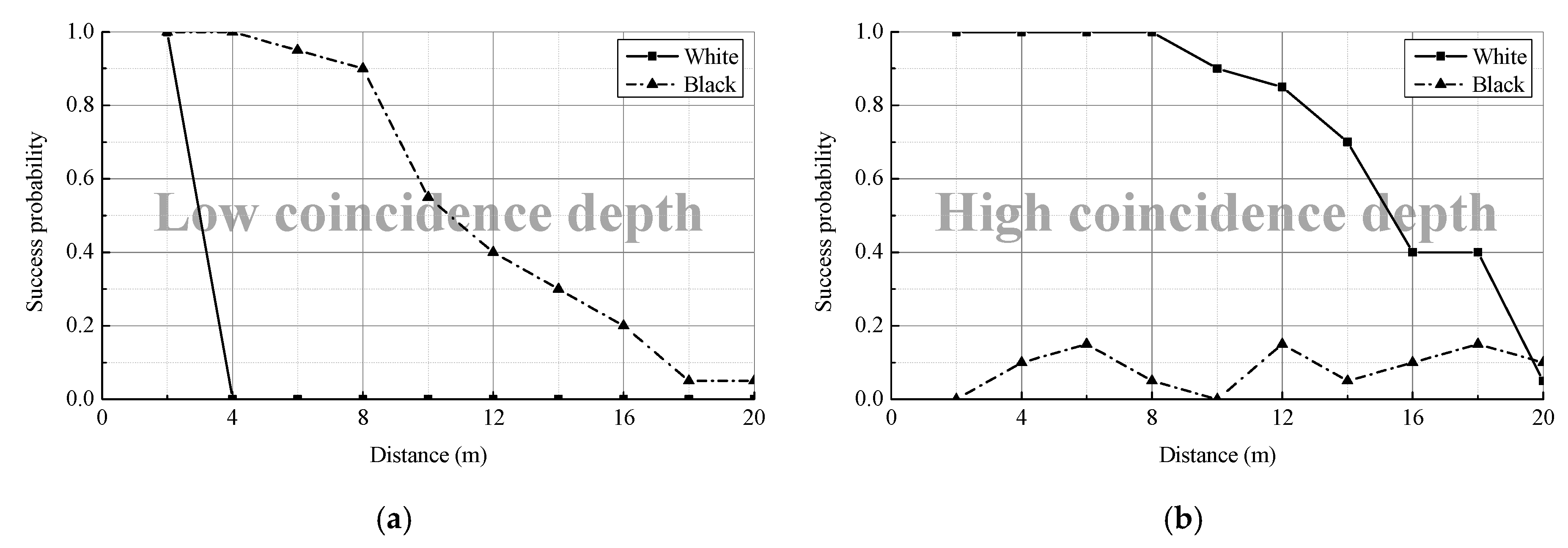
4. Measurements
5. Conclusions
Conflicts of Interest
References
- Remondino, F.; Stoppa, D. Tof Range-Imaging Cameras; Springer: New York, NY, USA, 2013; ISBN 978-3-642-27522-7. [Google Scholar]
- Perenzoni, M.; Perenzoni, D.; Stoppa, D. A 64 × 64-Pixels Digital Silicon Photomultiplier Direct TOF Sensor With 100-MPhotons/s/pixel Background Rejection and Imaging/Altimeter Mode With 0.14% Precision Up To 6 km for Spacecraft Navigation and Landing. IEEE J. Solid-State Circ. 2017, 52, 151–160. [Google Scholar] [CrossRef]
- Bronzi, D.; Villa, F.; Bellisai, S.; Markovic, B.; Tisa, S.; Tosi, A.; Zappa, F.; Weyers, S.; Durini, D.; Brockherde, W.; Paschen, U. Low-noise and large-area CMOS SPADs with timing response free from slow tails. In Proceedings of the 2012 Proceedings of the European Solid-State Device Research Conference (ESSDERC), Bordeaux, France, 17–21 September 2012; pp. 230–233. [Google Scholar]
- Portaluppi, D.; Conca, E.; Villa, F. 32 x 32 CMOS SPAD Imager for Gated Imaging, Photon Timing, and Photon Coincidence. IEEE J. Sel. Top. Quantum Electron. 2018, 24, 1–6. [Google Scholar] [CrossRef]
- Niclass, C.; Soga, M.; Matsubara, H.; Ogawa, M.; Kagami, M. A 0.18-µm CMOS SoC for a 100-m-Range 10-Frame/s 200 x 96-Pixel Time-of-Flight Depth Sensor. IEEE J. Solid-State Circ. 2014, 49, 315–330. [Google Scholar] [CrossRef]
- Beer, M.; Hosticka, B.J.; Kokozinski, R. SPAD-based 3D sensors for high ambient illumination. In Proceedings of the 2016 12th Conference on Ph.D. Research in Microelectronics and Electronics (PRIME), Lisbon, Portugal, 7–30 June 2016; pp. 1–4. [Google Scholar]
- Beer, M.; Schrey, O.M.; Hosticka, B.J.; Kokozinski, R. Coincidence in SPAD-based time-of-flight sensors. In Proceedings of the 2017 13th Conference on Ph.D. Research in Microelectronics and Electronics (PRIME), Giardini Naxos, Italy, 12–15 June 2017; pp. 381–384. [Google Scholar]
- Bronzi, D.; Tisa, S.; Villa, F.; Bellisai, S.; Tosi, A.; Zappa, F. Fast Sensing and Quenching of CMOS SPADs for Minimal Afterpulsing Effects. IEEE Photon. Technol. Lett. 2013, 25, 776–779. [Google Scholar] [CrossRef]

Publisher’s Note: MDPI stays neutral with regard to jurisdictional claims in published maps and institutional affiliations. |
© 2018 by the authors. Licensee MDPI, Basel, Switzerland. This article is an open access article distributed under the terms and conditions of the Creative Commons Attribution (CC BY) license (https://creativecommons.org/licenses/by/4.0/).
Share and Cite
Beer, M.; Thattil, C.; F. Haase, J.; Ruskowski, J.; Brockherde, W.; Kokozinski, R. SPAD-Based LiDAR Sensor in 0.35 µm Automotive CMOS with Variable Background Light Rejection. Proceedings 2018, 2, 749. https://doi.org/10.3390/proceedings2130749
Beer M, Thattil C, F. Haase J, Ruskowski J, Brockherde W, Kokozinski R. SPAD-Based LiDAR Sensor in 0.35 µm Automotive CMOS with Variable Background Light Rejection. Proceedings. 2018; 2(13):749. https://doi.org/10.3390/proceedings2130749
Chicago/Turabian StyleBeer, Maik, Charles Thattil, Jan F. Haase, Jennifer Ruskowski, Werner Brockherde, and Rainer Kokozinski. 2018. "SPAD-Based LiDAR Sensor in 0.35 µm Automotive CMOS with Variable Background Light Rejection" Proceedings 2, no. 13: 749. https://doi.org/10.3390/proceedings2130749
APA StyleBeer, M., Thattil, C., F. Haase, J., Ruskowski, J., Brockherde, W., & Kokozinski, R. (2018). SPAD-Based LiDAR Sensor in 0.35 µm Automotive CMOS with Variable Background Light Rejection. Proceedings, 2(13), 749. https://doi.org/10.3390/proceedings2130749