Abstract
The effect of water wave impacts and breakdown on the output performance of Water-Dielectric Single Electrode Mode Triboelectric Nanogenerators (WDSE-TENG) has been evaluated. When water contacts a TENG consisting of a hydrophobic dielectric layer, the triboelectric effect is generated with a net negative charge on the dielectric material and net positive charge on the water surface. The hydrophobic dielectric materials, which show the highest electrical output performance in contact with water, were FEP, silicone rubber and polyimide. The average output power of each sample for a load resistance of 10 MΩ was found to be in the range 14.69 to 19.12 µW. The results demonstrate that WDSE-TENG devices can work as an alternative energy harvesting mechanism by using water as a triboelectric material.
1. Introduction
Ocean wave energy has attracted great interest as a source of electrical energy for many years. Effective utilization and sustainability of this kind of energy can be exploited due to the effects of climate change with the rapid increase of sea levels and more recurrent flooding in coastal zones. Specifically, the cumulative loads of wave impact forces at coastal defence structures deliver high magnitude pulse-like forces with a wide frequency range of destructive oscillatory compressed air bubbles at the structure-water interfaces in the range of 30 to 300 Hz with a pressure range of 50 to 350 Pa predicted through a fluid-structure simulation [1]. Such energy can be potentially harvested and exploited using WDSE-TENG that converts the external mechanical energy into electricity by a combination of triboelectric effect and electrostatic induction, based on contact electrification between water and hydrophobic dielectric polymer films (Polydimethylsiloxane (PDMS), Polytetrafloroethylene (PTFE), silicone rubber, Fluorinated ethylene propylene (FEP) and Polyimide (Kapton)).
Traditionally, TENG are designed to work between solid materials in contact and they work well under dry conditions [2]. However, triboelectricity can exist when liquids are flowing through insulating tubes [3,4]. Therefore, in order to explore the opportunity to use water as one type of triboelectric material choice for TENG, a single electrode and split single electrode TENG prototypes were fabricated and characterized to study and analyze the contact electrification between water and the aforementioned dielectric polymer films. Which can derive an alternative and novel approach of energy harvesting for ocean wave monitoring applications that require self-powering in liquid environments. Potential applications include sensing at structure-water interfaces, such as those used to prevent critical damage in coastal defence systems.
2. WDSE-TENG Prototypes Fabrication and Electrical Characterization Measurements Set-Up
The fabricated WDSE-TENG prototypes have a triboelectric active area of 7 cm × 4 cm and three different configurations, as depicted in Figure 1, using hydrophobic dielectric layers with high negativity in the triboelectric series [5]. For the first WDSE-TENG a dielectric layer (PTFE (thickness (t = 100 µm), FEP (t = 25 µm), Silicone rubber (t = 150 µm) and PDMS (t = 125 µm)) was manually fixed with conductive glue on a copper layer (t = 100 µm), which acts as electrode. The other exposed side of the copper layer was insulated with black PTFE tape to protect it from the water to prevent a short circuit (Figure 1a). With this device configuration, the contact electrification occurs at the face of the dielectric layer in contact with water. For the second configuration a metal layer (Al (t = 18 µm), Cu (t = 100 µm)) was completely insulated within silicone rubber layers on both sides to protect it from the water (Figure 1b) and with the aim to increase the contact area to produce contact electrification in both faces of the device when the water contacts it. Additionally, using the second configuration, a copper layer was manually insulated on one side with a layer of PDMS and on the other side with a layer of PTFE with conductive acrylic adhesive (t = 25 µm) to test the combination of two different materials in contact electrification with water at the same time. For the electrical characterization, the electrode of each sample was connected to an external load of 10 MΩ.
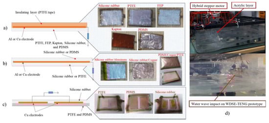
Figure 1.
Three configurations of fabricated WDSE-TENG prototypes (a) WDSE-TENG with one dielectric layer, (b) full device covered with two dielectric layers, and (c) split single electrode-two dielectric layers in contact with water. (d) WDSE-TENG prototypes placed on the water wave generator tank for their output performance measurements on water conditions.
The third configuration comprised two copper layers (split electrode) with an active area of 2.5 cm × 3 cm and a separation distance of 8 mm, which were manually fixed with conductive acrylic adhesive on a dielectric layer (PTFE (t = 100 µm), PDMS (t = 125 µm)). The other face of the device was insulated with a layer of silicone rubber to protect it from short-circuit in contact with water (Figure 1c). The contact electrification will be produced on both faces of the device when it contacts the water with the two electrodes connected to an external load of 10 MΩ for the electrical characterization with the objective to increase the charge transfer between the split electrode compared with the WDSE-TENG. The complete fabrication process was performed at room temperature.
The WDSE-TENG output performance of the prototypes was characterized using a water wave generator tank in order to replicate the conditions of the mechanical energy generated by ocean wave impact. A hybrid stepper motor (RS Pro 535-0502, RS Components Ltd., Corby, UK) attached with an acrylic layer of 20 cm × 20 cm (t = 8 mm) is used to generate the water waves motion into the water tank at different frequencies mounted on the left side of the tank. The WDSE-TENG devices were placed at the wall on the right side of the tank where the water wave breaks (at a frequency of 1.20 Hz) against the wall facing the impact of the water wave with the dielectric triboelectric layer, which generates interchange of triboelectric charges between both surfaces as shown in Figure 1d. All the WDSE-TENG prototypes and connection wires were insulated to avoid short circuit when the devices get in contact with water. The output voltage measurements were obtained with a digital oscilloscope Tektronix TDS 2014C (Premier Farnell Limited, Leeds, UK). The output current and output power of the DMSE-TENG measurements were performed using an Agilent Technologies N6705B Power analyzer (Premier Farnell Limited, Leeds, UK).
3. Experimental Results and Discussion
Figure 2 illustrates the contact electrification between the water wave and the hydrophobic dielectric layers and also the working mechanism of the WDSE-TENG, which can be explained as a result of contact electrification and electrostatic induction. Before the dielectric layer makes contact with water (Figure 2a), no charge transfer occurs. When the water wave starts to contact against the dielectric layer (Figure 2b), the ionization of the surface groups on the dielectric layer will cause the dielectric layer to be negatively charged [6] and create a positively charged electrical double layer (EDL) on the contact surface of the water wave to maintain electrical neutrality [7,8] (Figure 2c). As the water wave breaks down and moves off the dielectric layer, the positive charges in the EDL can be carried away with the water and the negative charges can remain on the surface of the dielectric layer. The negative electric potential difference between the electrode and load resistor (10 MΩ) to the ground attains equilibrium as electrons flow to ground (Figure 2d). This process produces an instantaneous negative current due to the triboelectric charges on the dielectric layer, which can be retained for a long time. When another water wave makes contact with the negatively charged dielectric layer, the negative charges will attract counter ions from the water to form another positively charge EDL, and establishes a positive electric potential difference. Therefore, electrons will flow from ground and load resistor to the electrode (Figure 2e) until reaching a new equilibrium (Figure 2f). This process produces an instantaneous positive current. When the water wave breaks down and leaves the dielectric layer, a negative electric potential difference will be established between the electrode and load resistor to the ground and another new equilibrium is achieved (Figure 2g). Once the following water wave contacts with the dielectric layer of the WDSE-TENG prototype (Figure 2a–g), a continuous output will be obtained. The water wave after the impact with the dielectric layer of the WDSE-TENG prototype should not leave residual water on the dielectric hydrophobic layer surface, in an ideal situation with the objective to generate the maximum electrical output.
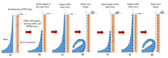
Figure 2.
Working mechanism of the WDSE-TENG prototypes by the contact electrification of dielectric layers with water wave impact. (a) Before the dielectric layer makes contact with water, no charge transfer occurs. (b) The ionization of the surface groups on the dielectric layer will cause the dielectric layer to be negatively charged and (c) create a positively charged EDL on the contact surface of the water wave to maintain electrical neutrality. (d) The negative electric potential difference attains equilibrium as electrons flow to ground. (e) When another water wave contacts the negatively charged dielectric layer, establishes a positive electric potential difference as electrons will flow to the electrode, (f) until reaching a new equilibrium. (g) When the water wave breaks down and leaves the dielectric layer, another new equilibrium is achieved. (a–g) Once the following water wave contacts the WDSE-TENG prototype, a continuous output will be obtained.
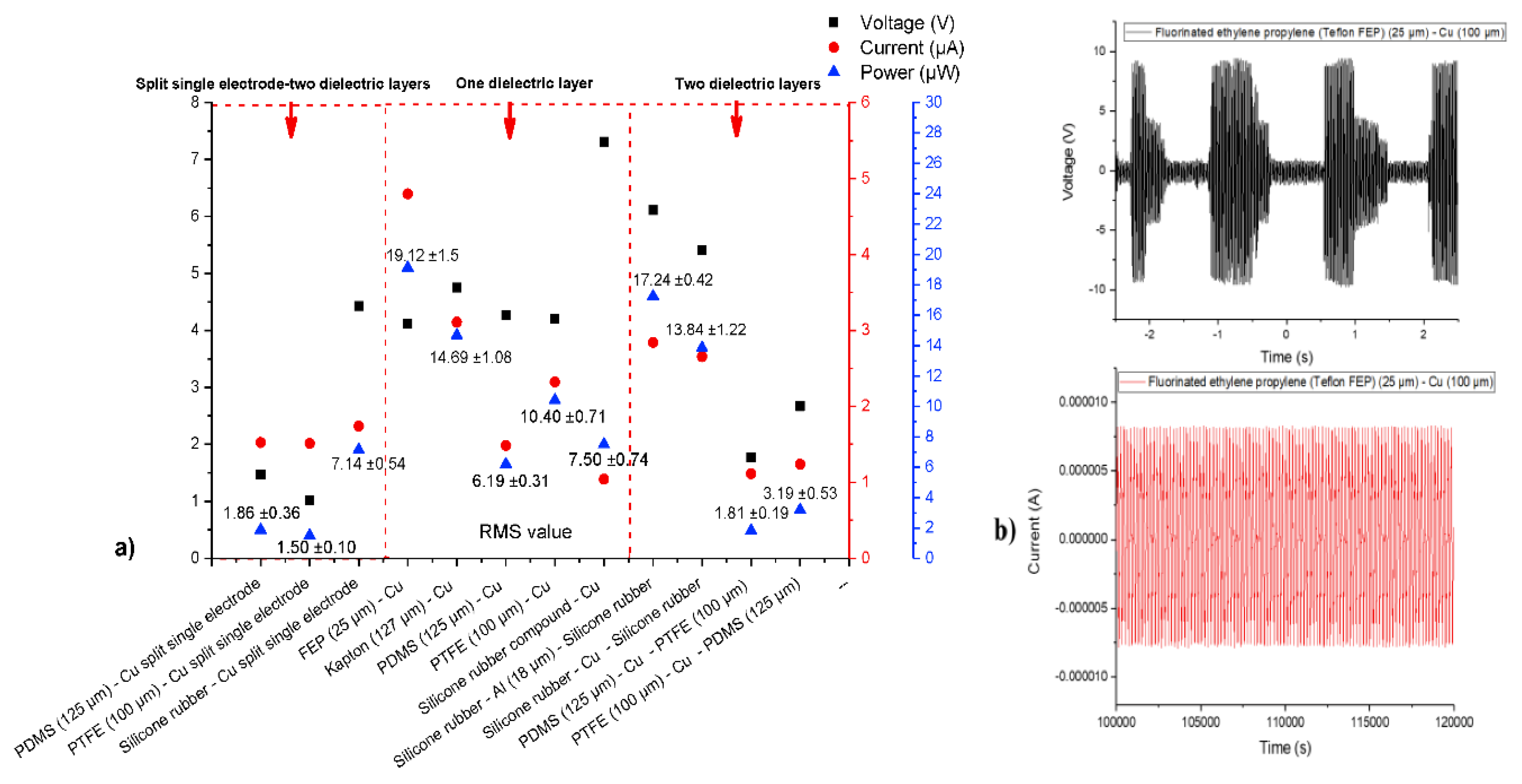
The comparison of the three configurations for the WDSE-TENG energy harvester prototypes according to their electrical output performance measurements is shown in Figure 3a. The average output power (1.5 µW to 20 µW) was calculated from the measured VRMS (1 V to 7.3 V) and IRMS (1 µA to 5 µA) of the proposed devices. The WDSE-TENG with one dielectric layer using FEP (t = 25 µm) in contact with water produced the highest output power of 19.12 µW, which corresponds to a VRMS of 4.11 V and an IRMS of 4.80 µA (Figure 3b). The prototype with two dielectric layers of silicone rubber and aluminum as electrode produced the next highest output power, likely due to the large contact area (VRMS, IRMS and power of 7.31 V, 2.84 µA and 17.24 µW, respectively). However, the output performance decreased for the WDSE-TENG with split single electrode due to the reduced active area of 2.5 cm × 3 cm. Furthermore, the configuration of the WDSE-TENG with two distinct dielectric layers of PDMS and PTFE shown relatively poor output power performance (Figure 3a).
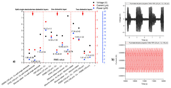
Figure 3.
(a) Comparison of the output voltage (VRMS), current (IRMS) and average output power of the WDSE-TENG prototypes with three configurations exposed to 1.2 Hz water wave impact. (b) Instantaneous output voltage (V) and current (I) of the WDSE-TENG using a FEP dielectric layer.
4. Conclusions
In summary, the output performance measurements have demonstrated the potential of the proposed WDSE-TENG prototypes for harvesting mechanical energy from ocean wave impact forces at the structure-water interfaces using water as a triboelectric active material. These new devices can work in liquid environments and hence can provide an energy source for sensing. Further investigation is required to explore suitable designs and efficient energy coupling to enhance the WDSE-TENG output performance employing the hydrophobic dielectric layers that shows a highest performance in contact with water.
Acknowledgments
We thank CONACYT for the fellowship awarded to Ulises Tronco Jurado.
Conflicts of Interest
The authors declare no conflict of interest.
References
- Mayon, R.B. Investigation of Wave Impacts on Porous Structures for Coastal Defences. In Proceedings of the 12th International Conference on Hydrodynamics (ICHD), Delft, The Netherland, 18–23 September 2016. [Google Scholar]
- Zhu, G.; Lin, Z.H.; Jing, Q.; Bai, P.; Pan, C.; Yang, Y.; Zhou, Y.; Wang, Z.L. Toward large-scale energy harvesting by a nanoparticle-enhanced triboelectric nanogenerator. Nano Lett. 2013, 13, 847–853. [Google Scholar] [CrossRef] [PubMed]
- Ravelo, B.; Duval, F.; Kane, S.; Nsom, B. Demonstration of the triboelectricity effect by the flow of liquid water in the insulating pipe. J. Electrost. 2011, 69, 473–478. [Google Scholar] [CrossRef]
- Paillat, T.; Touchard, G. Electrical charges and liquids motion. J. Electrost. 2009, 67, 326–334. [Google Scholar] [CrossRef]
- Diaz, A.; Felix-Navarro, R. A semi-quantitative tribo-electric series for polymeric materials: The influence of chemical structure and properties. J. Electrost. 2004, 62, 277–290. [Google Scholar] [CrossRef]
- Choi, D.; Lee, H.; Kang, I.S.; Lim, G.; Kim, D.S.; Kang, K.H. Spontaneous electrical charging of droplets by conventional pipetting. Sci. Rep. 2013, 3, 2037. [Google Scholar] [CrossRef] [PubMed]
- Lyklema, J. Fundamentals of Interface and Colloid Science: Soft Colloids; Elsevier: Amsterdam, The Netherlands, 2005; Volume 5. [Google Scholar]
- Lin, Z.H.; Cheng, G.; Lee, S.; Pradel, K.C.; Wang, Z.L. Harvesting Water Drop Energy by a Sequential Contact-Electrification and Electrostatic-Induction Process. Adv. Mater. 2014, 26, 4690–4696. [Google Scholar] [CrossRef] [PubMed]

Publisher’s Note: MDPI stays neutral with regard to jurisdictional claims in published maps and institutional affiliations. |
© 2018 by the authors. Licensee MDPI, Basel, Switzerland. This article is an open access article distributed under the terms and conditions of the Creative Commons Attribution (CC BY) license (https://creativecommons.org/licenses/by/4.0/).