Nanofabrication of SOI-Based Photonic Waveguide Resonators for Gravimetric Molecule Detection †

 ,
,  ,
, 
Abstract
:1. Introduction
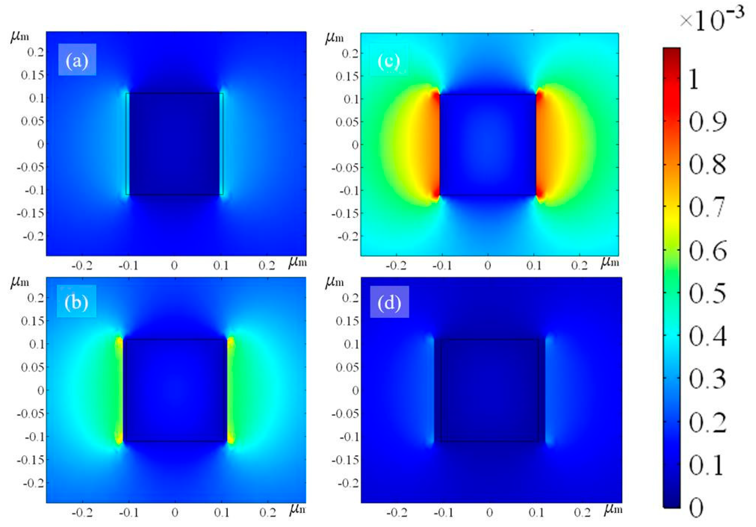
2. Simulations
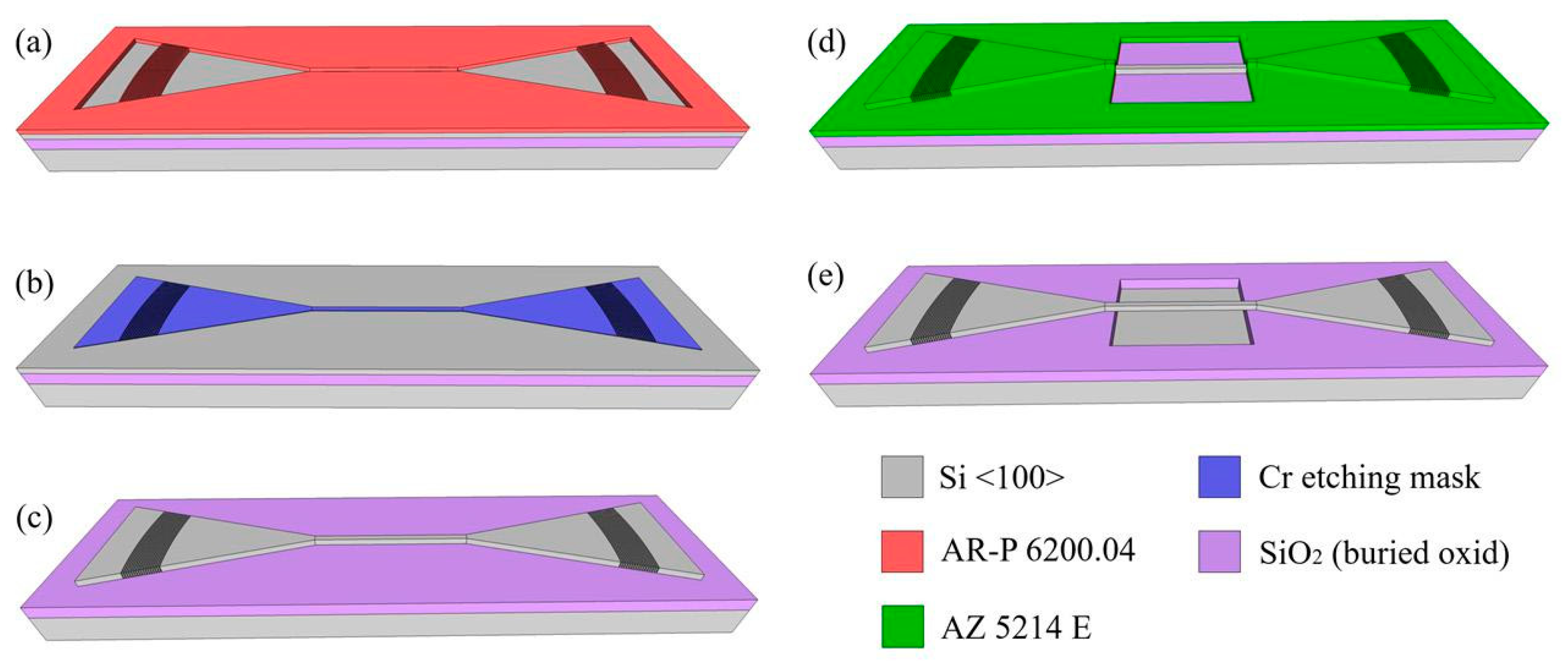
3. Nanofabrication
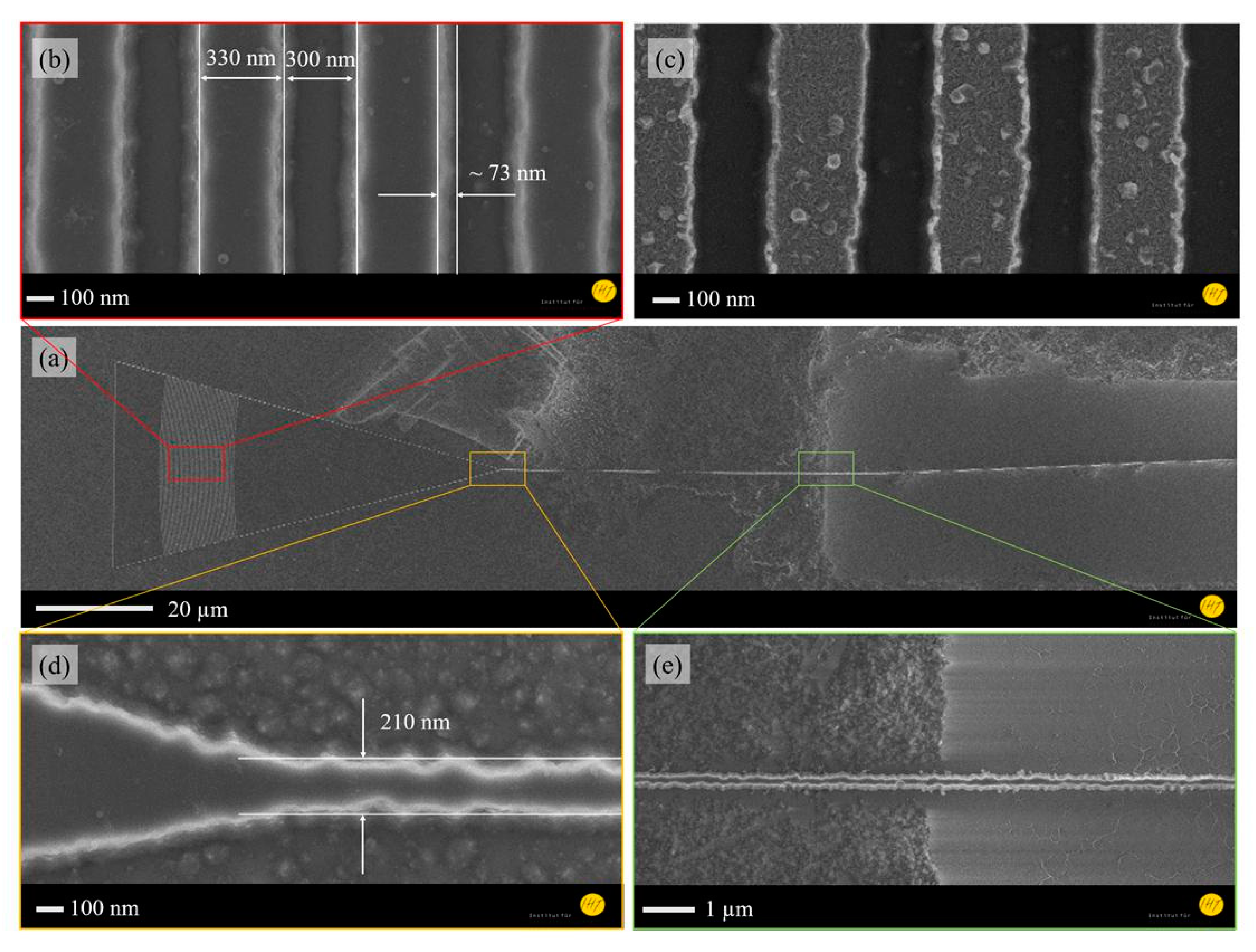
4. Results and Discussion
Author Contributions
Acknowledgments
Conflicts of Interest
References
- Lim, A.E.-J.; Song, J.; Fang, Q.; Li, C.; Tu, X.; Duan, N.; Chen, K.K.; Tern, R.P.-C.; Liow, T.-Y. Review of silicon photonics foundry efforts. IEEE J. Sel. Top. Quantum Electron. 2014, 20, 8300112. [Google Scholar] [CrossRef]
- Wasisto, H.S.; Merzsch, S.; Uhde, E.; Waag, A.; Peiner, E. Handheld personal airborne nanoparticle detector based on microelectromechanical silicon resonant cantilever. Microelectron. Eng. 2015, 145, 96–103. [Google Scholar] [CrossRef]
- Wasisto, H.S.; Merzsch, S.; Waag, A.; Uhde, E.; Salthammer, T.; Peiner, E. Airborne engineered nanoparticle mass sensor based on a silicon resonant cantilever. Sens. Actuator B 2013, 180, 77–89. [Google Scholar] [CrossRef]
- Wasisto, H.S.; Merzsch, S.; Steib, F.; Waag, A.; Peiner, E. Vertical silicon nanowire array-patterned microcantilever resonators for enhanced detection of cigarette smoke aerosols. Micro Nano Lett. 2014, 9, 676–679. [Google Scholar] [CrossRef]
- Wasisto, H.S.; Merzsch, S.; Stranz, A.; Waag, A.; Uhde, E.; Salthammer, T.; Peiner, E. Femtogram aerosol nanoparticle mass sensing utilising vertical silicon nanowire resonators. Micro Nano Lett. 2013, 8, 554–558. [Google Scholar] [CrossRef]
- Wasisto, H.S.; Merzsch, S.; Stranz, A.; Waag, A.; Uhde, E.; Salthammer, T.; Peiner, E. Silicon nanowire resonators: Aerosol nanoparticle mass sensing in the workplace. IEEE Nanotechnol. Mag. 2013, 7, 18–23. [Google Scholar] [CrossRef]
- Rakich, P.; Reinke, C.; Camacho, R.; Davids, P.; Wang, Z. Giant enhancement of stimulated Brillouin scattering in the subwavelength limit. Phys. Rev. 2012, X2, 011008. [Google Scholar] [CrossRef]
- Qiu, W.; Rakich, P.; Soljacic, M.; Wang, Z. Stimulated Brillouin Scattering in Nanoscale Silicon Step-index Waveguides: A General Framework of Selection Rules and Calculating SBS Gain. Opt. Express 2013, 21, 31402–31419. [Google Scholar] [CrossRef] [PubMed]
Publisher’s Note: MDPI stays neutral with regard to jurisdictional claims in published maps and institutional affiliations. |
© 2019 by the authors. Licensee MDPI, Basel, Switzerland. This article is an open access article distributed under the terms and conditions of the Creative Commons Attribution (CC BY) license (https://creativecommons.org/licenses/by/4.0/).
Share and Cite
Granz, T.; Böke, J.S.; Hamdana, G.; Martens, M.; Misra, A.; Preußler, S.; Schilling, M.; Peiner, E.; Schneider, T.; Waag, A. Nanofabrication of SOI-Based Photonic Waveguide Resonators for Gravimetric Molecule Detection. Proceedings 2018, 2, 1055. https://doi.org/10.3390/proceedings2131055
Granz T, Böke JS, Hamdana G, Martens M, Misra A, Preußler S, Schilling M, Peiner E, Schneider T, Waag A. Nanofabrication of SOI-Based Photonic Waveguide Resonators for Gravimetric Molecule Detection. Proceedings. 2018; 2(13):1055. https://doi.org/10.3390/proceedings2131055
Chicago/Turabian StyleGranz, Tony, Julia Sophie Böke, Gerry Hamdana, Michael Martens, Arijit Misra, Stefan Preußler, Meinhard Schilling, Erwin Peiner, Thomas Schneider, and Andreas Waag. 2018. "Nanofabrication of SOI-Based Photonic Waveguide Resonators for Gravimetric Molecule Detection" Proceedings 2, no. 13: 1055. https://doi.org/10.3390/proceedings2131055
APA StyleGranz, T., Böke, J. S., Hamdana, G., Martens, M., Misra, A., Preußler, S., Schilling, M., Peiner, E., Schneider, T., & Waag, A. (2018). Nanofabrication of SOI-Based Photonic Waveguide Resonators for Gravimetric Molecule Detection. Proceedings, 2(13), 1055. https://doi.org/10.3390/proceedings2131055