Abstract
The core facility of the Wakasa Wan Energy Research Center (WERC) consists of three ion accelerators: a synchrotron, a tandem accelerator and an ion-implanter. Research on the irradiation effects using these accelerators has been performed on space electronics such as solar cells, radiation detectors, image sensors and LSI circuits. In this report, the accelerator facility and ion-irradiation apparatuses at WERC are introduced, focusing on the research on irradiation effects on space electronics. Then, some recent results are summarized.
1. Introduction
The Wakasa Wan Energy Research Center (WERC) opened in November 1998, and from July 2000, an accelerator facility which forms the core of WERC became available. The accelerator facility consists of three accelerators: a synchrotron, a tandem accelerator and an ion-implanter [1,2]. Using these accelerators, we have been involved in research on the destruction of tumor cells in human bodies (proton beam radiotherapy) [3,4], the transmutation of DNAs in plants and bacteria (ion beam breeding) [5,6,7], ion beam material modification [8,9,10] and ion beam analysis for materials [11,12,13]. The accelerators at WERC have also been utilized to simulate the radiation effects on materials which are related to nuclear power plants [14,15,16] and those of space electronics [17,18,19,20,21,22,23,24,25]. Electronic systems are severely affected by the radiation environment in space. There are three main irradiation effects on space electronics: the single event effect (SEE), the total ionizing dose effect (TID) and the displacement damage dose effect (DDD) [26,27,28,29,30,31]. Before the operation of electronic devices in space, these effects from the radiation environment in space have to be evaluated on earth. Recently, the space industry has been widespread; therefore, the radiation tolerance of space electronics has been actively investigated using electron, gamma-ray, and ions. In this report, we describe the specification of each accelerator, beam lines, and irradiation apparatuses at WERC, focusing on the research of the radiation effects for space electronics. Since the three accelerators can cover a wide energy range of ions from 10 keV to 660 MeV, we can simulate the space radiation field well. Finally, several recent research results of the ion irradiation effects on solar cells, LSI circuits, radiation detectors and image sensors are summarized.
2. Overview of Ion Accelerators at WERC
Figure 1 shows the layout of two ion sources, the tandem accelerator, the synchrotron, the ion-implanter, and their beam transport lines at WERC [1,2]. The tandem accelerator is interfaced to the synchrotron, and used as an injector for the synchrotron. The synchrotron can accelerate protons up to 200 MeV. Such a high energy proton beam has been used mainly for the study of SEE on space electronic devices at irradiation room 4. The tandem accelerator has also been used independently to accelerate protons up to 10 MeV. This medium energy proton beam has been used for the study of TID and DDD on image sensors at irradiation room 2. The ion-implanter provides 10 to 200 keV ions with high beam current. This low energy and intense beam has been used for research of DDD on solar cells at irradiation room 1. The detailed specification of each accelerator will be explained in the following subsections.
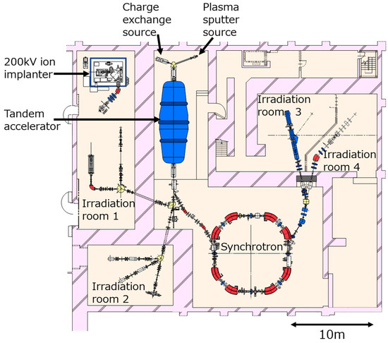
Figure 1.
Layout of two ion sources, the tandem accelerator, the synchrotron, the ion-implanter, and their beam transport lines at WERC [1,2].
2.1. Tandem Accelerator at WERC
The tandem accelerator at WERC (Figure 2) accelerates negative ions which are injected from the two ion sources alternatively. One of the ion sources is a plasma sputter type source, and it generates hydrogen ions and heavy ions such as carbon ions. The typical peak intensity of pulsed negative hydrogen ions, which are used for the proton acceleration by the synchrotron, is 4 mA with a 20 Hz period and 25 μs duration. The other ion source is a kind of charge exchange type for the ionization of gas elements. Especially, the highly intense 4He negative ion beam, the current of which amounts to 40 μA, enables α particle irradiation with a high-density energy deposition into target materials.
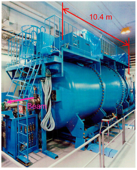
Figure 2.
Tandem accelerator at WERC.
The acceleration voltage of the tandem accelerator amounts up to 5 MV. The high tension is generated by the Schenkel circuit with a 58-step voltage doubler rectifier, which rectifies 40 kHz RF power by a resonant transformer and an oscillator. The Schenkel rectifier, the acceleration tube, the high-tension terminal, and the resonant transformer are sustained by the insulation column support in the pressure tank. The pressure tank is filled with SF6 insulation gas at 0.6 MPa gauge. In order to enable the acceleration of the highly intense beam from the ion sources, the conveyor current through the Schenkel rectifier amounts to 1 mA at the terminal high tension of 5 MV. The voltage ripple is 0.4 kVpp at the terminal high tension of 5 MV.
The charge exchange canal in the terminal has an inner diameter of 15 mm and a charge exchange effective length of about 1 m. Although the diameter of 15 mm seems to be large, the geometrical transmission efficiency is about 70% because of the large emittance of the negative ion from the ion sources. Argon gas for the charge exchange (stripper gas) is introduced into the middle of the canal. A differential pumping and the recirculation by four turbo-molecular pumps, each with a pumping speed of 50 L/s, enable the concentration of stripper gas in the canal with a large inner diameter. Such a stripper gas system realizes the 99% conversion of negative ions to positive at a gas thickness of 4 Pa·m. Additionally, the transmission efficiency along the following transport beam line to the synchrotron is achieved to be almost perfect. Therefore, a pulsed proton beam with peak intensity of 3 mA can be injected into the synchrotron. Table 1 summarizes the specifications of the tandem accelerator at WERC.

Table 1.
Specifications of tandem accelerator.
2.2. Synchrotron
A proton beam with a maximum energy of 10 MeV is injected from the tandem accelerator into the synchrotron and is accelerated up to 200 MeV. Recently, for the proton acceleration, the injection energy has been set at 7 MeV.
The overview of the synchrotron at WERC is shown in Figure 3. The circumference of the synchrotron is 33.2 m. The super periodicity is 4. Each lattice has a QF-BM-QD-BM permutation, and is operated in separated function style. Here, QF and QD are focusing and defocusing quadrupole magnets in the median plane, respectively, and BM means a bending magnet. Horizontal and vertical tunes are 1.75 and 0.85, respectively. A period of 2 s for the synchrotron acceleration consists of four modes of “injection and capture”, “acceleration”, “extraction”, and “deceleration, then return to injection”. The injection is performed in a multi-turn injection style. The RF knock out system slowly extracts the accelerated beam out of the separatrix in the horizontal phase space. The separatrix is generated by the excitation of sextupole magnets. By adjusting the RF strength by time, the variation in the intensity of the extracted beam by time is controlled to be reduced for event-by-event mode experiments such as a counter performance test and SEE investigations on semiconductor devices. The usual range of the beam intensity for the irradiation of space electronic devices is from 0.1 to 3 nA. Table 2 tabulates the principal specifications of the synchrotron at WERC.
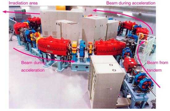
Figure 3.
Synchrotron at WERC.
Table 2.
Specifications of synchrotron.
2.3. Ion-Implanter
A high current ion beam irradiation equipment named the 200 kV ion-implanter has been installed at WERC for research on the radiation effects of materials related to atomic power plants and of space electronics. This accelerator has also been utilized for the modification of semiconductors and metallic alloys. The schematic diagram of the 200 kV ion-implanter are shown in Figure 4.
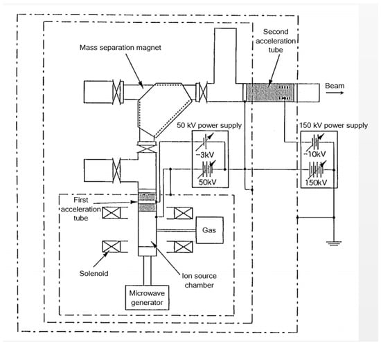
Figure 4.
The schematic diagram of 200 kV ion-implanter at WERC.
The 200 kV ion-implanter consists of a microwave ion source, a 50 kV first acceleration tube, a mass separation magnet, and a 150 kV second acceleration tube. The microwave ion source supplies positive ions from gas targets, such as H2, He, N2, Ne, Ar, etc. Positive ions generated in the ion source are accelerated up to 50 keV by the first acceleration tube. Then, they are sorted by mass with the mass separation magnet. In the case of the H2 gas target, we can select H+ or H2+ by changing the magnet field of the mass separator. After the mass separation, the ions are accelerated again up to 200 keV by the second acceleration tube. The ion energy can be changed from 10 to 200 keV. The maximum beam currents available from the first and the second acceleration tubes are 50 and 30 mA, respectively. In the actual irradiation experiments, however, the beam current is reduced to less than several tens of micro A/cm2 to avoid beam heating of the target materials during the irradiation.
3. Beamlines and Irradiation Apparatuses for the Research on Irradiation Effects on Space Electronics
3.1. Beamline of the Synchrotron in Irradiation Room 4
In irradiation room 4, we can perform irradiation experiments with ion beams extracted from the synchrotron. Figure 5 shows the layout of the beam line in irradiation room 4. After an ion beam is accelerated by the synchrotron and transported to irradiation room 4, the beam is deflected to the direction of the target samples by a bending magnet and is shaped by two sets of quadrupole magnet doublets. Then, the ion beam is emitted into the atmosphere through a copperized polyimide thin film window. In order to form the appropriate irradiation field on the target surface, the ion beam is wobbled by a set of wobbling magnets and/or scattered by a tungsten scatterer and collimated by a brass block collimator.

Figure 5.
Beam line in irradiation room 4.
The intensity distribution of the cross section of the primary proton beam at 200 MeV kinetic energy has almost an axially symmetrical Gaussian shape with around 1.5 cm standard deviation about beam direction. We call this beam as “pencil beam”. The usual irradiation area on the sample is within 2 cm by 2 cm squares; therefore, the pencil beam covers the irradiation area with a flatness (the ratio of intensity at the edge of the irradiation area to that at the center) of more than 80%. Sometimes, much more severe uniformity is required to the intensity distribution. In such case, we use a tungsten scatterer with a thickness of 0.1 mm to make a flatness of more than 94%.
In TID experiments, the beam intensity amounts to around 3 nA, which corresponds to a flux of 2.5 × 108 cm−2s−1 in the case of an irradiation area of 2 cm by 2 cm squares and a scatterer thickness of 0.1 mm. In experiments for the single event effect (SEE), the ion beam flux is required to be reduced to less than 1 × 107 cm−2s−1. Thus, the beam intensity is reduced to 0.1 nA by adjusting the strength of the RF kicker. In order to obtain a beam flux of less than 1 × 106 cm−2s−1, a thicker scatterer is used for the reduction in the area density of the beam.
The proton beam can be spread to large targets, such as a 10 cm by 10 cm square for instance. SEE experiments with a flux of less than 106 cm−2s−1 can be performed by using only the scatterer to form a large irradiation field. In the case of 107 cm−2s−1 flux experiment, the beam is wobbled by a set of wobbling magnets to improve the beam utilization efficiency.
In several SEE experiments, the cross section for the SEE occurrence is measured as a function of the linear energy transfer (LET) of primary beam in the target material. In order to perform the experiment, the energy of the projectile has to be changed for each LET value. Although the beam energy from the synchrotron is variable, the excitation pattern of all magnets and acceleration RF, and beam transport setup have to be changed for each beam energy. Therefore, an energy degrader is used instead of a conventional method for the variation of the beam energy. The degrader, made of resin which is water-equivalent in the proton energy loss, can change its thickness in units of 1 mm from 2 to 270 mm. The degrader is set at a position immediate upstream of the irradiation target.
An ionization chamber (shown as “dose monitor” in Figure 5) is used for the dose control. As the ionization efficiency relates to a function of the energy deposition by passing particles, the dose measured by the ionization chamber is calibrated for each energy variation by measuring the beam current at the beam dump. The probability of the recombination of ion-electron pairs is a function of density of the pairs produced in the ionization chamber. Therefore, the calibration of the dose monitor is also performed for each variation of beam intensity and irradiation area by the comparison between the averaged current signals from the dose monitor and beam dump for 3~5 times measurements. The doses are controlled with an error (standard deviation) of almost 2% and 1% for the 100 MeV proton irradiation to the area of 10 cm by 10 cm with flux of 3 × 10⁶ and 1 × 107 cm−2s−1, respectively.
The synchrotron beam is used to measure the radiation effects not only on space electronics but also on radiation detectors to be used in space for astronomical phenomena. As usual detectors count each particle and/or gamma/X-ray, the charged particle energy and flux under the circumstances around the space probe have to be simulated. In these experiments, the beam intensity is reduced to less than 10 kHz. The intensity is controlled by the charged particle counting using a counter-telescope with two sets of plastic scintillators read by photomultiplier tubes.
3.2. Beamline of the Tandem Accelerator in Irradiation Room 2
The ion beam extracted from the tandem accelerator is not only injected into the synchrotron system but is also directly transported to irradiation room 1 and 2. Three beam lines are installed in irradiation room 2. One of the beam lines is used for the research on irradiation effects on space electronics. Hydrogen (H), helium (He), carbon (C), nickel (Ni), and copper (Cu) ions are available for the irradiation experiments. The beam line consists of two scanning magnets and two apertures; it ends with an irradiation chamber with high and cold temperature sample stages with three-axis goniometers. Figure 6 shows the beam line and the irradiation chamber. Ion beams are injected into the irradiation chamber from the back to the front in the figure. A sample stage on the goniometer can be moved about 60 mm horizontally and about 45 mm vertically with a precision of less than 0.05 mm and rotated 180° about the horizontal axis with a precision of less than 0.05°. The shape of the beam is checked using a fluorescent plate which is placed on the sample stage. The beam diameter on the sample stage can be reduced to less than 10 mm. To ensure a homogeneous irradiation for large area targets, ion beams are scanned horizontally with a frequency of 50 Hz and vertically with a frequency of 0.1–5.0 Hz by the scanning magnets with the continuous triangle waveform current. The irradiation can be performed at high (20 to 700 °C) or cold (−173 to 20 °C) temperatures. The temperature on the sample stages is measured by a thermocouple. The maximum setting area of samples is 60 × 60 mm2 on the sample stage. H and He beams can be scanned over the above area. The scan area for Ni beams is narrower than the light ion cases because Ni is much heavier than H or He. The horizontal and vertical scan widths for a 10 MeV Ni3+ beam are 24 and 20 mm at maximum, respectively. The degree of vacuum in the irradiation chamber is less than 9 × 10⁻⁴ Pa, even during the irradiation. Electronic device samples can be wired in the chamber via electrical feedthroughs to measure the electronic characteristics of the devices during the irradiation.
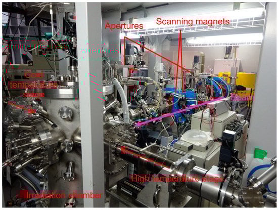
Figure 6.
Beamline and irradiation chamber for the irradiation of space electronics in irradiation room 2.
3.3. Beamline of the 200 kV Ion-Implanter in Irradiation Room 1
The ion beam accelerated by the ion-implanter in irradiation room 1 is manipulated using a bending magnet and three quadrupole magnets. The beam size is defined by X-Y slits (shown in Figure 7). The beam can be uniformly spread up to 10 cm squares. The performances of the 200 kV ion-implanter are summarized in Table 3. An irradiation chamber has five sample stages (Figure 8, left). Three of them have a heating system, and the sample temperature can be controlled from room temperature to 1000 °C during the irradiation. The other two sample stages have a water cooling system, which can keep samples around room temperature even during the irradiation. To check the beam uniformly, a fluorescence plate is set at the bottom of the target stages (Figure 8, right). An aperture for defining the beam shape and a –500 V secondary electron suppresser are placed in front of each sample stage. The beam current on the sample stage is measured by a pico-ammeter.
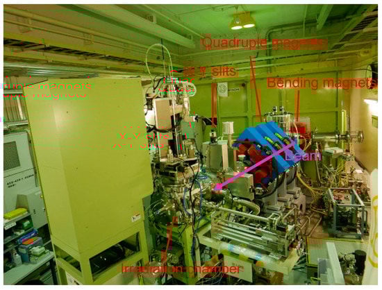
Figure 7.
Beamline and irradiation chamber of the ion-implanter.
Table 3.
Performance of the 200 kV ion-implanter.
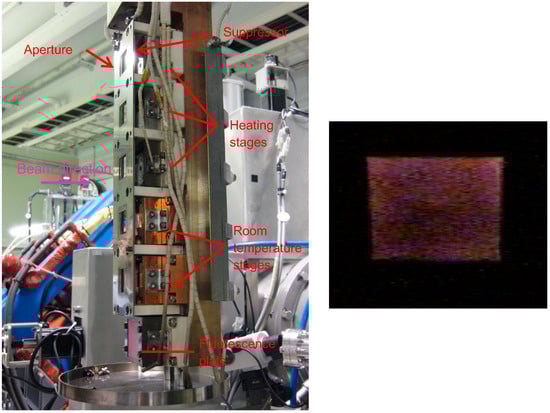
Figure 8.
Sample stages (left), and captured image of the fluorescence plate for beam irradiation (right).
4. Recent Results of Ion Irradiation Effects on Space Electronics at WERC
4.1. Recent Experiments Using Accelerators at WERC
Many radioactive sources exist in space such as electrons, X/γ-ray, and ions. Protons are the main ion component in space; thus, ion irradiation effects are investigated mainly using proton beam. Typical beam currents for irradiation experiments are ~1 nA, ~100 nA, and 1–10 µA, for the synchrotron, the tandem, and the ion-implanter, respectively. The synchrotron is used usually for research on SEE because high energy proton beam can simulate the high-density electronic excitation by the space radiation. On the other hand, the medium energy proton beam from the tandem accelerator is used for research on TID/DDD. The low energy ion beam with a high intensity from the ion-implanter is used exclusively for research on DDD. A lot of irradiation experiments for space electronics have been performed using the three accelerators at WERC. These experiments are summarized in Table 4. We introduce some experiments in the following sections.
Table 4.
Summary table of irradiation experiments for space electronics at WERC.
4.2. Research Results Using the Synchrotron
In the X/gamma ray astronomy field, various X/gamma ray detectors and electronic circuits dedicated to the detectors, which are durable in space, have been developed. One of the detectors uses a CMOS (complementary metal-oxide semiconductor) imaging sensor. The CMOS sensor can be driven with a small power consumption since the signal transmission is not accompanied by charge transfer and high voltage analog circuits are not needed, such as CCD (charge-coupled device) sensors. The CMOS sensor is chip-integrable together with its peripheral circuit; therefore, it is possible to reduce the size and cost of the detector. For such a reason, the CMOS image sensor has been adopted especially for usage in small space probes.
HiZ-GUNDAM [32] is a future satellite mission for the exploration of the early universe by detecting high-redshift gamma-ray bursts by using the wide-field X-ray detector. The Kanazawa University group will adopt a CMOS image sensor GSENSE6060BSI fabricated by Gpixel Inc. for the detection of soft X-ray [17]. The radiation tolerance test was conducted using GSENSE400BSI-TVISB, which is close in pixel size and has the same resistivity and epilayer thickness as GSENSE6060BSI. The test for the sensor was performed by the irradiation of a 100 MeV proton with a flux of 1 × 107 cm−2s−1 and a fluence of 4.8 × 1010 cm−2, which corresponds to the absorbed dose of 5 krad during 6 years in orbit. After the irradiation, the energy spectra of Mn-Kα and Kβ X-ray were obtained at temperatures of +20 °C and −20 °C (Figure 9). Although the significant damage appears as the increase in the dark noise and the worsening of the energy resolution, the background tail of the low energy side caused by the dark noise is reduced in the operation at −20 °C (Figure 9, right). Although the MOS structure seems to be affected by TID, the increase in dark current noise is considered to be caused by bulk damage from DDD.
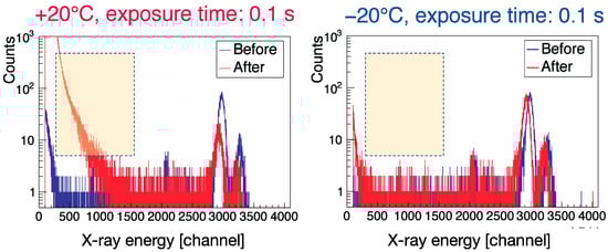
Figure 9.
Comparison of the Mn-Kα and Kβ spectra obtained before and after the 100 MeV proton irradiation. Although the noise tail appears on the low-energy side at +20 °C, after cooling of sample to −20 °C, contribution of dark noise is significantly reduced. (Reprint Figure 10 in p.5 of N. Ogino et al., Nucl. Inst. and Methods in Phys. Research, A987(2021) 164843).
The Hiroshima University group has chosen a system of a CsI(Tl) scintillator and a silicon photomultiplier (Si-PM) for the X/gamma ray detector onboard CubeSats. The Si-PM is a kind of avalanche photodiode (APD) and the multi pixelated Si-PM (Multi Pixel Photon Counter, MPPC) were supplied by Hamamatsu Photonics K.K. (HPK). Two types of MPPCs (S13360-6050CS and S14160-6050HS) were irradiated with a 200 MeV proton beam. Figure 10 shows the comparison between the gamma ray spectra obtained several minutes and 7 months after the 300 rad irradiation. Just after the irradiation, the 22.2 keV photo peak from 109Cd (blue line) disappears in the spectrum and the threshold level rises. In the gamma ray spectrum measured after the MPPC that was left at room temperature for 7 months, the recovery of 22.2 keV photo peak can be found in the spectrum. It is a certain annealing effect against the irradiation for the MPPC [18].
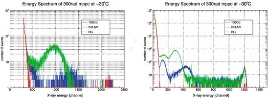
Figure 10.
Gamma-ray spectra with MPPC S13360-6050CS at −30 °C. Left figure is acquired at several minutes after 300 rad irradiation and right figure shows the spectra measured at 7 months after irradiation. (Reprint Figure 4 in p.3 of N. Hirade et al., Nucl. Inst. and Meth. in Phys. Research A986(2021) 164673).
Not only radiation detectors but also electronic devices such as a power module, integrated circuits used in an analog amplifier, a logic gate, a microcomputer, etc. have to be evaluated for the radiation tolerance. The gate oxide structure of MOSFET (metal-oxide semiconductor field effect transistor) and IGBT (insulated gate bipolar transistor) used in the power module is subject to the TID effect. SEE may also be observed as the single event upset (SEU) in the switching device by the charged particle-induced ionization in the depletion layer. Especially, SEE in IGBT in the power module and CMOS in the logic gate with a parasitic thyristor in themselves may generate single event latchup (SEL), causing the thermal runaway. Once SEE occurs in the gate region of power MOS-FET or IGBT, the destruction of the gate may cause another thermal runaway, i.e., single event burnout (SEB).
The Tokyo Institute of Technology group has developed APD X-ray detectors and their dedicated ASIC (application-specific integrated circuit). The 0.35 μm CMOS technology is used for the developed ASIC. The ASIC has dual interlock cell (DICE) circuits with a master–slave flip-flop’s scheme to prevent malfunction due to the distortion or the noisy clock signal and the accidental activation of CMOS, i.e., an SEU event. The evaluation test of the radiation tolerance was performed for the ASIC with 90 MeV protons because the threshold and saturation energies for the cross section of SEE in the logic device have been reported to be set at around 10 MeV and 100 MeV, respectively. The proton beam was directly irradiated on the ASIC with a flux of 4.8 × 10⁷ s−1cm−2 and a fluence of 1.0 × 1011 cm−2, which corresponds to the total dose for 160 years in the International Space Station (ISS) orbit [19]. During the irradiation, the currents from the positive and negative power supplies for the charge sensitive amplifier (CSA) on the ASIC were monitored in order to check whether an SEL event occurred or not. The digital bit data of DICEs were duplicated on a copy register in order to detect SEU events during the irradiation. There was no indication of an SEL event and any SEU events were not obtained either. The ASIC has 1030-bit registers; therefore, the SEU cross-section is estimated to be 2.2 × 10⁻¹⁴ cm2bit−1 at most.
The Kyushu Institute of Technology group has tried to obtain the excitation function of the SEE cross section by the variation of kinetic energy of proton [20]. The measurements were conducted for the microchips of PIC16F877, Raspberry Pi Zero and Raspberry Pi 3B. The obtained excitation function shows that the threshold energy for SEE in the integrated circuits may be set at around 10 MeV.
The Aoyama Gakuin University and Nagoya University group have paid attention to the radiation effect on the detectors in space from the radioactivation point of view. A gamma-ray detector using new scintillator LaBr3 (Ce) has been developed for the CALorimetric Electron Telescope (CALET) experiment on ISS. LaBr3 (Ce) detectors were irradiated with 20, 70, and 140 MeV protons with fluences of 7.9 × 10¹⁰, 7.1 × 10⁹, and 5.0 × 109 cm−2, respectively [21]. After the irradiation, the activation of the scintillators was investigated by measuring gamma-ray energy spectra by Ge detectors.
4.3. Research Results Using the Tandem Accelerator and the Synchrotron
An AlGaN/GaN high-electron mobility transistor (HEMT) has a lot of advantages for space applications, such as having high efficiency, high power and being lightweight. In order to quantify the radiation tolerance of the HEMT in space environment, Sasaki et al. investigated the change in its device characteristics by using the 11.1 MeV, 20.6 MeV and 66.8 MeV proton beams from the synchrotron [22]. The irradiation was performed with the proton flux of 1.7 × 108 cm−2s−1 under off-bias (Vgs = −5.0 V, Vds = 100 V) condition. No difference was observed in the breakdown voltage at any irradiation energy (Figure 11).
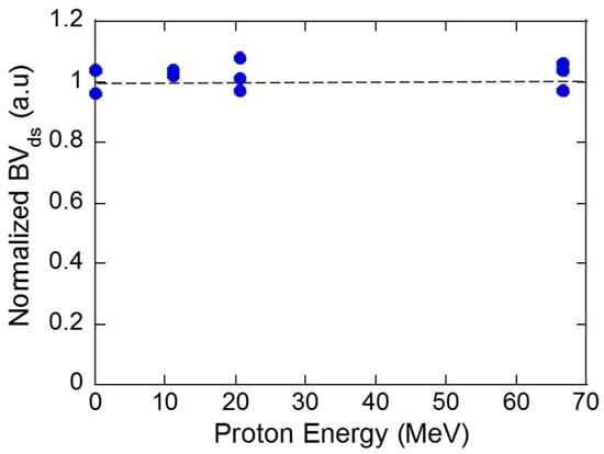
Figure 11.
Normalized off-state (Vgs = −5.0 V) drain breakdown voltage (BVds) of HEMT under 11.1–66.8 MeV proton irradiation.
To study the DDD effect on the HEMT, the change in the output power due to the 2 MeV proton irradiation was also examined by using the tandem accelerator [22]. The 2 MeV proton beam flux was 7 × 1011 cm−2s−1. The output power at last decreased by −4 dB and −10 dB at fluences of 3 × 10¹⁴ and 1 × 1015 cm−2, respectively (Figure 12). Sasaki et al. have explained this irradiation effect as being due to the lattice defects produced by the proton irradiation. As the effect by proton fluence of 7 × 10¹¹/cm2 roughly corresponds to the radiation damage of 10 years in the geostationary orbit, the experimental result indicates that this device has a sufficient margin for proton irradiation tolerance to operate in the geostationary orbit. They have also found that when the channel temperature was 125 °C, the output power was partially recovered by radio frequency (RF) operation or reverse bias stress (Vgs = −5 V, Vds = 30 V).
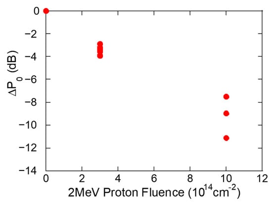
Figure 12.
Change in output power of HEMT by 2 MeV proton irradiation.
4.4. Research Results Using the Tandem Accelerator
The Martian Moons eXploration (MMX) is a project of the Japan Aerospace Exploration Agency (JAXA) to explore the two moons (Phobos and Deimos) of Mars with a scheduled launch in the mid-2020s. A spacecraft will enter into the orbit around Mars and will collect scientific data and gather samples from the moons’ surfaces. Unlike the Earth, Mars does not have a global magnetic field. Therefore, electronic devices attached to the MMX spacecraft orbiting around Mars and its moons will be exposed to interplanetary high energy protons with the wide energy range. Ozaki et al. have performed the experiments on irradiation resistance evaluation of CCD imagers, which is one of the important electronic devices installed to the MMX spacecraft, by using an 8 MeV proton beam from the tandem accelerator [23]. The irradiation effect has been observed as an increase in dark current. They have performed a similar experiment using a 70 MeV proton beam at another facility. From the proton energy dependence of the irradiation effect on CCD imagers, the experimental data are now being analyzed in terms of the total ionization dose (TID) and the non-ionization energy loss (NIEL).
4.5. Research Results Using the Ion-Implanter
As perovskite solar cells have beneficial features as a high-power conversion efficiency as high as 24%, low-cost, thin-coating, lightweight, and large-area fabrication, they are expected for the application to the space industry. To confirm the irradiation effect on perovskite type solar cells, Kanaya et al. performed the 50 keV proton irradiation with total doses of 1 × 10¹³, 1 × 10¹⁴, and 1 × 1015 cm−2 using the 200 kV ion-implanter [24]. To investigate the irradiation effect on the grain structure and lattice structure, three types of perovskite solar cells with different grain sizes (~240, ~340, and ~690 nm) were used and the irradiation effects were evaluated by a scanning electron microscope (SEM), X-ray diffraction (XRD), photoluminescence (PL), and time-resolved photoluminescence (TRPL). From the experimental results of SEM and XRD, they have concluded that there is little difference between the initial and irradiated samples in the grain structure or the crystal structure. The result of the TRPL spectrum measurements is shown in Figure 13. Even by the irradiation up to the fluence of 1 × 1014 cm−2, the TRPL spectrum curve does not exhibit a significant decrease. After the irradiation with the fluence of 1 × 1015 cm−2, the lifetime of TRPL spectrum decreases for each grain size. The experimental result shows that perovskite solar cells have a high radiation resistance against the proton irradiation up to the fluence of 1014 cm−2.
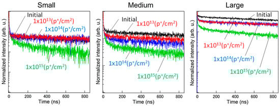
Figure 13.
Effect of 50 keV proton irradiation on normalized TRPL decay curves for small grain (~240 nm) sample, medium grain (~340 nm) sample, and large grain (~690 nm) sample. (Reprint Figure 2 in p. 6992 of S. Kanaya et al., J. Phys. Chem. Lett. 10(2019) 6990–6995).
Triple-junction (InGaP/InGaAs/Ge) solar cells are typical successors for the space application and currently widely utilized due to their higher photovoltaic conversion efficiency and better radiation resistance compared to conventional single-junction silicon space solar cells. Imaizumi et al. investigated the effects of the fluence rate and the irradiation mode (defocused beam or scanned beam) of 50, 100 and 150 keV proton irradiation ground tests on the degradation of a triple-junction solar cell and a single-junction silicon solar cell using two accelerators: the ion-implanter at WERC, and that at the National Institutes for Quantum and Radiological Science and Technology (QST)-Takasaki. They have found that the photovoltaic properties of both the solar cells are degraded irrespective of the fluence rate or the irradiation mode. The details are discussed in [25].
Finally, we mention the study of the proton irradiation effect on carbonaceous chondrites by Nakauchi et al. [33]. Although this study is not directly related to the irradiation effect on space electronics, the result obtained by the ion irradiation at WERC is academically quite interesting and important in the field of the astrophysics.
Airless planetary bodies, from which carbonaceous chondrites (CCs) originate, have been mainly exposed to the irradiation with solar wind protons. To investigate the effect of solar wind protons on the surfaces of planetary bodies, Nakauchi et al. irradiated serpentine and saponite samples, which are two major components of CCs, with 10 keV H2+ ions up to the fluence of 1.7 × 10¹⁸ protons/cm2, and their reflectance spectra were measured in the wavelength range from 1.5 to 5.5 μm. As the 10 keV H2+ molecule ion becomes two 5 keV proton ions at the sample surface by the Coulomb explosion process, the 10 keV H2+ ion irradiation corresponds to the 5 keV proton irradiation. Figure 14 shows that the absorption strength for serpentine at the wavelengths of 2.85 μm and 3.0 μm increases with increasing the proton dose. The absorption at 2.85 μm and that at 3.0 μm correspond to Si-OH and the total amount of OH and H2O, respectively. This experimental result is the first direct evidence of H2O formation at the surfaces of airless planetary bodies only by solar wind protons.
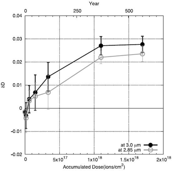
Figure 14.
Change in absorption strength at 2.85 μm and 3.0 μm as a function of proton dose for serpentine. (Reprint Figure 6 in p.6 of Y. Nakauchi et al., Icarus 355(2021) 114140).
5. Summary
The ion accelerator facility at WERC, which consists of three kinds of accelerators (the synchrotron, the tandem accelerator, and the ion-implanter), has been utilized for the ground tests of the irradiation-induced degradation of several space electronics such as space solar cells, radiation detectors, image sensors, and LSI circuits. The facility has also contributed to the fundamental study on the astrophysics. Through collaborations with several universities, private companies, and national institutes such as JAXA and QST, further research and development using the ion facility at WERC can be expected for the space industry.
Author Contributions
Original draft preparation, writing and editing, S.H., R.I. and K.S. Final check of draft, K.K. All authors have read and agreed to the published version of the manuscript.
Funding
This research received no external funding.
Data Availability Statement
The data presented in this study are available on request from the authors.
Acknowledgments
The authors thank Yonetoku, Ogino, Takahashi, Yatsu, Arimoto, Yamaoka, Okumaya, Sasaki, Ozaki, Kanaya, and Nakauchi for their great help. The authors also thank T. Ohshima and M. Imaizumi for fruitful discussion.
Conflicts of Interest
The authors declare no conflict of interest.
References
- Hatori, S.; Kurita, T.; Hayashi, Y.; Yamada, M.; Yamada, H.; Mori, J.; Hamachi, H.; Kimura, S.; Shimoda, T.; Hiroto, M.; et al. Developments and applications of accelerator system at the Wasasa Wan Energy Research Center. Nucl. Instrum. Methods B 2005, 241, 862–869. [Google Scholar] [CrossRef]
- Hatori, S.; Fukumoto, S.; Hayashi, Y.; Kagawa, H.; Kurita, T.; Minehara, E.J.; Nagasaki, S.; Nakata, Y.; Odagiri, T.; Shimada, M.; et al. Tandem accelerator as an injector for the medical-use synchrotron at the wakasa wan energy research center. In Proceedings of the 1st International Particle Accelerator Conference, Kyoto, Japan, 23–28 May 2010; pp. 714–716. [Google Scholar]
- Fujinaga, H.; Sakai, Y.; Yamashita, T.; Arai, K.; Terashima, T.; Komura, T.; Seki, A.; Kawaguchi, K.; Nasti, A.; Yoshida, K.; et al. Biological characteristics of gene expression features in pancreatic cancer cells induced by proton and X-ray irradiation. Int. J. Radiat. Biol. 2019, 95, 571–579. [Google Scholar] [CrossRef]
- Lin, C.; Kume, K.; Mori, T.; Martinez, M.E.; Okazawa, H.; Kiyono, Y. Predictive Value of Early-Stage Uptake of 3’-Deoxy-3’-18F-Fluorothymidine in Cancer Cells Treated with Charged Particle Irradiation. J. Nucl. Med. 2015, 56, 945–950. [Google Scholar] [CrossRef]
- Das, S.K.; Masuda, M.; Hatashita, M.; Sakurai, A.; Sakakibara, M. Optimization of culture medium for cordycepin production using Cordyceps militaris mutant obtained by ion beam irradiation. Process Biochem. 2010, 45, 129–132. [Google Scholar] [CrossRef]
- Takagi, K.; Tsukada, T.; Izumi, M.; Kazama, K.; Hayashi, Y.; Abe, T. Localization of γH2AX Fluorescence along Tracks of Argon Beams. RIKEN Accel. Prog. Rep. 2010, 43, vii–viii. [Google Scholar]
- Hatashita, M.; Takagi, K.; Ichida, H.; Abe, T. Effect of ion-beam irradiation on mycelial growth of medicinal mushrooms. RIKEN Accel. Prog. Rep. 2019, 53, 200. [Google Scholar]
- Ito, Y.; Yamauchi, T.; Yamamoto, A.; Sasase, M.; Nishio, S.; Yasuda, K.; Ishigami, R. Ion beam synthesis of 3C-SiC layers in Si and its application in buffer layer for GaN epitaxial growth. Appl. Surf. Sci. 2004, 238, 159–164. [Google Scholar] [CrossRef]
- Ishigami, R.; Batchuluun, C.; Yasuda, K. Increase in coercivity of Fe-Pt thin film permanent magnets by N2+ ion implantation and heat treatment in hydrogen gas. Nucl. Instrum. Methods B 2012, 275, 58–62. [Google Scholar] [CrossRef]
- Iwase, A.; Yoneda, K.; Ishigami, R.; Matsui, T. Restoration of ion beam irradiation induced metastable magnetic states and lattice structures of FeRh thin films by heat treatments at elevated temperatures. J. Magn. Magn. Mater. 2020, 515, 167286. [Google Scholar] [CrossRef]
- Yasuda, K.; Kajitori, Y.; Oishi, M.; Nakamura, H.; Haruyama, Y.; Saito, M.; Suzuki, K.; Ishigami, R.; Hibi, S. Upgrades of a time-of-fight elastic recoil detection analysis measurement system for thin flm analysis. Nucl. Instrum. Methods B 2019, 442, 53–58. [Google Scholar] [CrossRef]
- Suzuki, K.; Nakata, Y. Development of an in-air ERDA system for hydrogen analysis. Nucl. Instrum. Methods B 2019, 450, 135–138. [Google Scholar] [CrossRef]
- Suzuki, K.; Tsuchiya, B.; Yasuda, K.; Nakata, Y. Light element analysis of ceramics using in-air ERDA and TOF-ERDA. Nucl. Instrum. Methods B 2020, 478, 169–173. [Google Scholar] [CrossRef]
- Fukumoto, K.; Tone, K.; Onitsuka, T.; Ishigami, R. Effect of Ti addition on microstructural evolution of V–Cr–Ti alloys to balance irradiation hardening with swelling suppression. Nucl. Mater. Energy 2018, 15, 122–127. [Google Scholar] [CrossRef]
- Das, A.K.; Ishigami, R.; Kamal, I. Proton implantation effect on SUS-316 stainless steel. J. Alloys Compd. 2015, 629, 319–321. [Google Scholar] [CrossRef]
- Fukumoto, K.; Kitamura, Y.; Miura, S.; Fujita, K.; Ishigami, R.; Nagasaka, T. Irradiation Hardening Behavior of He-Irradiated V-Cr-Ti Alloys with Low Ti Addition. Quantum Beam Sci. 2021, 5, 1. [Google Scholar] [CrossRef]
- Ogino, N.; Arimoto, M.; Sawano, T.; Yonetoku, D.; Yu, P.; Watanabe, S.; Hiraga, J.S.; Yuhi, D.; Hatori, S.; Kume, K. Performance verification of next-generation Si CMOS soft X-ray detector for space applications. Nucl. Instrum. Methods A 2021, 987, 164843. [Google Scholar] [CrossRef]
- Hirade, N.; Takahashi, H.; Uchida, N.; Ohno, M.; Torigoe, K.; Fukazawa, Y.; Mizuno, T.; Matake, H.; Hirose, K.; Hisadomi, S.; et al. Annealing of proton radiation damages in Si-PM at room temperature. Nucl. Instrum. Methods A 2021, 986, 164673. [Google Scholar] [CrossRef]
- Arimoto, M.; Harita, S.; Sugita, S.; Yatsu, Y.; Kawai, N.; Ikeda, H.; Tomida, H.; Isobe, N.; Ueno, S.; Mihara, T.; et al. Development of a 32-channel ASIC for an X-ray APD detector onboard the ISS. Nucl. Instrum. Methods A 2018, 882, 138–147. [Google Scholar] [CrossRef]
- Okuyama, K.; (Hitachi Ltd., Ibaraki-ken, Japan). Personal communication, 2021.
- Mizushima, T.; Yoshida, A.; Yamaoka, K.; Hatori, S.; Kume, K. Study on possible protpn-induced background of LaBr3(Ce) scintillator in a low-earth orbit. Proc. SPIE 2020, 11454, 114542S. [Google Scholar]
- Sasaki, H.; Hisaka, T.; Kadoiwa, K.; Kamo, Y.; Ishimura, E.; Hatori, S.; Ishigami, R.; Kume, K. Reliability Study of Proton Irradiation Effects on AlGaN/GaN HEMTs. In Proceedings of the 34th Annual Reliability of Compound Semiconductors (ROCS) Workshop, Minneapolis, MN, USA, 29 April 2019; pp. 83–86. [Google Scholar]
- Ozaki, M.; (Kobe University, Kobe, Japan). Personal communication, 2021.
- Kanaya, S.; Kim, G.M.; Ikegami, M.; Miyasaka, T.; Suzuki, K.; Miyazawa, Y.; Toyota, H.; Osonoe, K.; Yamamoto, T.; Hirose, K. Proton Irradiation Tolerance of High-Efficiency Perovskite Absorbers for Space Applications. J. Phys. Chem. Lett. 2019, 10, 6990–6995. [Google Scholar] [CrossRef]
- Imaizumi, M.; Ohshima, T.; Yuri, Y.; Suzuki, K.; Ito, Y. Effects of beam conditions for ground irradiation tests on degradation of photovoltaic characteristics of space solar cells. Quantum Beam Sci. 2021; to be published. [Google Scholar]
- Ferlet-Cavros, V.; Massengill, L.W.; Gouker, P. Single Event Transients in Digital CMOS—A Review. IEEE Trans. Nucl. Sci. 2013, 60, 1767–1790. [Google Scholar] [CrossRef]
- Srour, J.R.; Palko, J.W. Displacement Damage Effects in Irradiated Semiconductor Devices. IEEE Trans. Nucl. Sci. 2013, 60, 1740–1766. [Google Scholar] [CrossRef]
- Makino, T.; Onoda, S.; Ohshima, T.; Kobayashi, D.; Ikeda, H.; Hirose, K. A Methodology for Reconstructing DSET Pulses from Heavy-Ion Broad-Beam Measurement. Quantum Beam Sci. 2020, 4, 15. [Google Scholar] [CrossRef]
- Kobayashi, D.; Hirose, K.; Sakamoto, K.; Okamoto, S.; Baba, S.; Shindou, H.; Kawasaki, O.; Makino, T.; Ohshima, T.; Mori, Y.; et al. Data-Retention-Voltage-Based Analysis of Systematic Variations in SRAM SEU Hardness: A Possible Solution to Synergistic Effects of TID. IEEE Trans. Nucl. Sci. 2020, 67, 328–335. [Google Scholar] [CrossRef]
- Imaizumi, M.; Nakamura, T.; Takamoto, T.; Ohshima, T.; Tajima, M. Radiation degradation characteristics of component subcells in inverted metamorphic triple-junction solar cells irradiated with electrons and protons. Prog. Photovolt. Res. Appl. 2017, 25, 161–174. [Google Scholar] [CrossRef]
- Hoeffgen, S.K.; Metzger, S.; Steffens, M. Investigating the Effects of Cosmic Rays on Space Electronics. Front. Phys. 2020, 8, 318. [Google Scholar] [CrossRef]
- Yonetoku, D.; Mihara, T.; Sawano, T.; Ikeda, H.; Harayama, A.; Takata, S.; Yoshida, K.; Seta, H.; Toyanago, A.; Kagawa, Y.; et al. High-z gamma-ray bursts for unraveling the dark ages mission HiZ-GUNDAM. Proc. SPIE 2014, 9144, 15–26. [Google Scholar]
- Nakauchi, Y.; Abe, M.; Ohtake, M.; Matsumoto, T.; Tsuchiyama, A.; Kitazato, K.; Yasuda, K.; Suzuki, K.; Nakata, Y. The formation of H2O and Si-OH by H2+ irradiation in major minerals of carbonaceous chondrites. Icarus 2021, 355, 114140. [Google Scholar] [CrossRef]


Publisher’s Note: MDPI stays neutral with regard to jurisdictional claims in published maps and institutional affiliations. |
© 2021 by the authors. Licensee MDPI, Basel, Switzerland. This article is an open access article distributed under the terms and conditions of the Creative Commons Attribution (CC BY) license (https://creativecommons.org/licenses/by/4.0/).