Article

Inductive Compensation of an Open-Loop IPT Circuit: Analysis and Design

by
Mario Ponce-Silva
*,
Alan R. García-García
,
Jaime Arau
,
Josué Lara-Reyes
and
Claudia Cortés-García
Tecnológico Nacional de México—CENIDET, Cuernavaca 62490, Mexico
*
Author to whom correspondence should be addressed.
Inventions 2023, 8(4), 104; https://doi.org/10.3390/inventions8040104
Submission received: 19 July 2023 / Revised: 7 August 2023 / Accepted: 14 August 2023 / Published: 17 August 2023
(This article belongs to the Special Issue Recent Advances and Challenges in Emerging Power Systems)

Abstract

:
The main contribution of this paper is the inductive compensation of a wireless inductive power transmission circuit (IPT) with resonant open-loop inductive coupling. The variations in the coupling coefficient k due to the misalignment of the transmitter and receiver are compensated with only one auxiliary inductance in the primary of the inductive coupling. A low-power prototype was implemented with the following specifications: input voltage Vin = 27.5 V, output power Po = 10 W, switching frequency f = 500 kHz, output voltage Vo = 12 V, transmission distance d = 1.5 mm. Experimental results varying the distance “d” with several values of the compensation inductor demonstrate the feasibility of the proposal. An efficiency of 75.10% under nominal conditions was achieved. This proposal is a simple compensation topology for wireless chargers of cellular phones presenting small distances between the transmitter and receiver.

1. Introduction

Nowadays, wireless power transmission (WPT) has become a trending research topic due to many applications involving no wired connections such as charging of electric vehicles, cell phones, hand tools, biomedical implants and portable electronics [1,2].
WPT has been used mainly in two applications—in the sending of information and electrical energy, or only for transmitting electrical energy. The second case shall be addressed in this work, with the aim of transmitting electrical power from a power supply to an electrical load, using a resonant inductive coupling [3,4,5].
WPT can be classified into two categories—far-field and near-field WPT. The far-field category refers to the transmission of a large amount of energy between two positions, e.g., sending energy by electromagnetic waves. Near-field WPT refers to the distance of transfer energy within the wavelength (λ) of the transmitter antenna [6,7,8]. This paper will focus on near-field WPT.
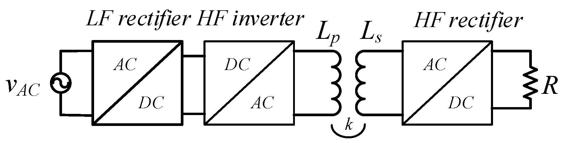
As shown in Figure 1, inductive power transmission (IPT) circuits consist of multiple stages of energy conversion to achieve the desired operation, usually as follows: low-frequency rectifier, high-frequency (HF) inverter with a resonant tank, inductive coupling with a coupling factor k, high-frequency rectifier, and load [9,10,11]. This work is focused on the stages from the HF inverter only.
An indispensable stage in IPT circuits is the resonant tank, also known as resonant network, which is an electrical circuit designed with capacitors and inductors which is capable of storing electrical energy and oscillating when it is operating at the resonant frequency. The circuit has zero reactance during the resonance condition, allowing the maximum transfer of power from a power supply to an electrical load with high efficiency [12,13].
In low-power resonant IPT applications, such as wireless chargers for smartphones and portable electronic devices (less than 20 W), the literature reports efficiencies of approximately 50–70% in open-loop operation and 70–80% in closed-loop operation [14,15].
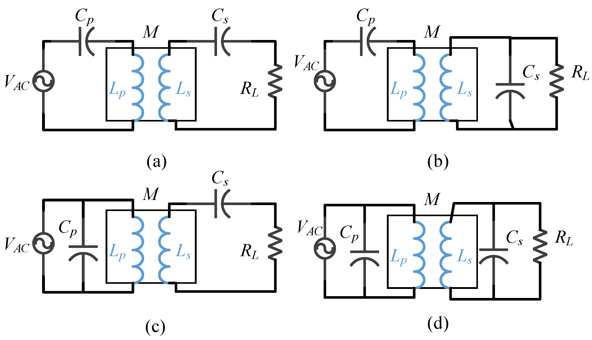
Usually, the IPT topologies require compensation networks to operate the circuit in resonance. The basic compensation networks are presented in Figure 2; as can be seen, the compensation networks include a capacitor in series or parallel with the transmitter and the receiver to compensate for their inductance and to operate at resonance [16,17].
The full circuit needs many components to achieve optimal operation; these components cause additional losses, thus diminishing the efficiency. One solution is to consider the parasitic components (leakage inductances) and use them as part of the design to achieve high efficiency, fewer components, and better power transfer in inductive coupling [18,19].
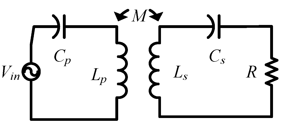
Many compensation topologies have been proposed to compensate for the leakage inductances. The most used compensation topologies consist of adding one capacitor in series with each leakage inductance Cp and Cs (Figure 3). Both capacitors are chosen to be in resonance with each leakage inductance [20,21,22].
Table 1 shows some reported circuits with their most important operating characteristics. This table shows that a higher operating power results in better overall efficiency of the circuit. In addition, Table 1 allows comparing the results obtained in this paper with those reported in the literature, where even though in this paper a low power of 10 W was used, an efficiency of up to 75% was achieved, which is higher than some of the circuits shown in Table 1 with similar power levels.
The main contribution of this paper is to eliminate the compensation capacitor Cs in the receiver, compensate for the misalignment of the transmitter and the receiver with only one series capacitor in the transmitter, and add an inductor in series with this capacitor to compensate for the changes in the mutual inductance M.
The proposal simplifies the secondary circuit and reduces the complexity of the circuit, with a higher efficiency than the works reported in Table 1. This contribution is particularly relevant in low-power applications where low size and cost are important, such as biomedical implants, portable electronics, electro mobility, and Internet of Things applications.

2. Analysis of the Circuit

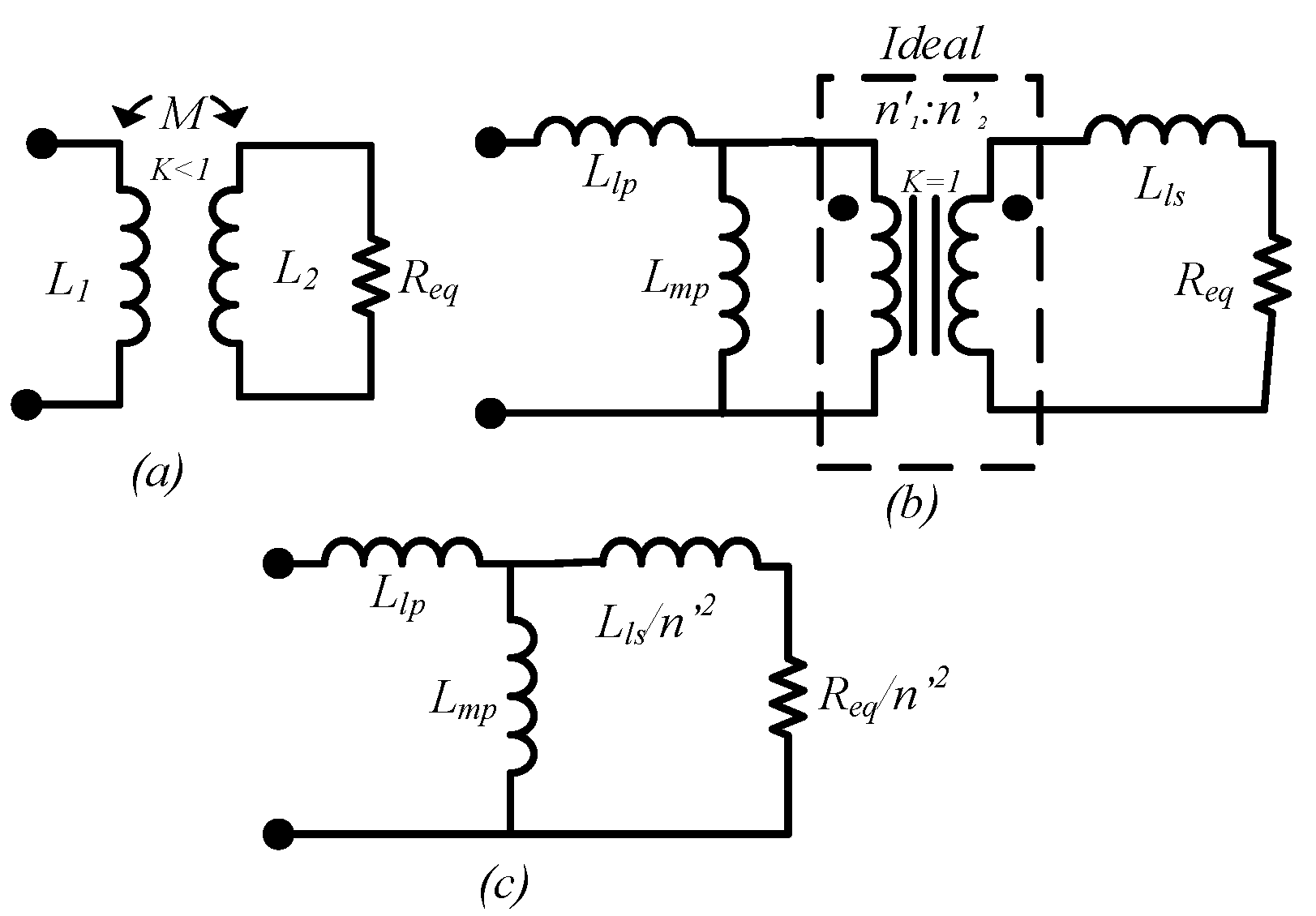
The IPT circuits are usually modelled as two coupled inductors as shown in Figure 4a, with a coupling factor k defined as:
k = M L 1 L 2
where M is the mutual inductance, L1 is the self-inductance of the primary (transmitter) and L2 is the self-inductance of the secondary (receiver). This model is commonly employed and useful in the literature.
The main disadvantage is that the model separates the analysis of the circuit into two parts—primary and secondary. To merge both circuits in only one, model T is the usual selection [31,32].
Model T could be rearranged as the circuit in Figure 4b. This circuit models the mutual inductance M as an ideal transformer with coupling factor k = 1 and turn relationship n’ = n’2/n’1; turns n’1 and n’2 represent the cross section of coils L1 and L2 that share the same common flux φM and are different from the total turn number of each inductor L1 (n1) and L2 (n2). The components of this model are related to the model in Figure 3b as shown in Table 2.
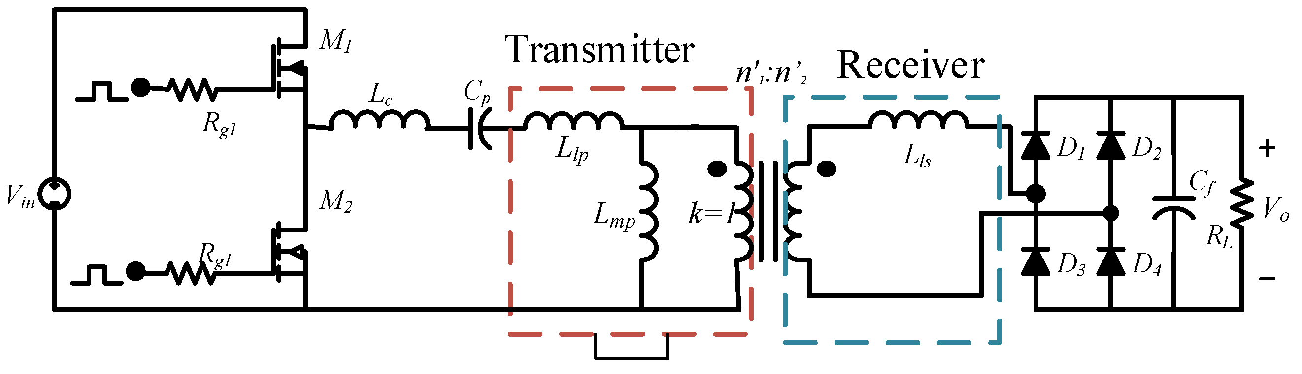
Figure 4c shows the elements of the secondary reflected to the primary of the ideal transformer; this last model was the model used in this analysis. The proposed circuit to be analyzed in this paper is presented in Figure 5. The HF inverter consists of a half bridge inverter with a compensation topology that is only made up of the compensation inductor LC and the capacitor Cp. The IPT transformer is modelled like the model in Figure 4b, where the HF AC–DC conversion consists of a conventional full bridge rectifier.
To compensate for the variations due to the misalignment of the transmitter and receiver, as well as variations caused by the increase in the distance between the transmitter and receiver, the compensation inductor Lc will have a value greater than 90% of the inductive reactance at resonant conditions. The remaining percentage of the inductive reactance belongs to the primary dispersion inductance Llp and the equivalent inductance Leq1 obtained from the inductive coupling.
To analyze the resonant network, the resonant converter shown in Figure 5 is simplified until an equivalent circuit is obtained in series, in which the resonance condition will be established. Figure 6 shows the simplification process.
Figure 6a shows that the half bridge inverter is modelled as the fundamental component of the square waveform Vin and the full bridge rectifier as a resistance Req1 that consumes the same average power. In Figure 6b, the leakage inductance of the receiver Lls and the equivalent resistance Req1 are reflected to the transmitter side, the equivalent impedance, in parallel with the primary magnetizing inductance Lmp, is reduced into an equivalent inductance and resistance Leq1 and Req2, and finally, all the inductances are reduced in only one inductor Leq2 (see Figure 6c).
The first step of the analysis is to obtain the equivalent resistance of the full bridge rectifier Req1. A simplified analysis is carried out in [33], which assumes that the efficiency of the rectifier is 100%. To improve accuracy, it is possible to consider a different value for the efficiency of the rectifier r) as follows:
η r = P o P R = P o 4 P D + P o
where Po is the power delivered to the load (RL) and PR is the power delivered to the rectifier stage.
With this consideration, the equivalent resistant Req1 is expressed as:
R e q 1 = 8 η r R L π 2
where RL is the load resistance.
As indicated in the introduction, the HF rectifier is one of the stages with higher losses. So, to minimize these losses, the efficiency of the rectifier is evaluated. To evaluate this efficiency, the following simplifications will be assumed:
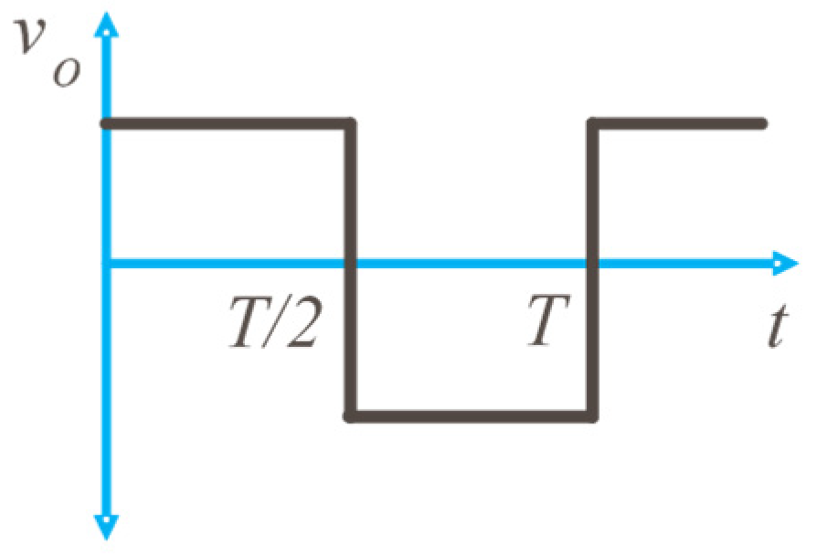
  • The voltage at the input of the full bridge rectifier (Vo) is a square waveform in phase with the current, similar to the waveform in Figure 7, where Vo is the output voltage in the load resistance.
  • The input current in the rectifier is a sinusoidal waveform. Therefore, the losses in one diode can be evaluated with Equation (4).
    P D = I D V f = I V f π
    where “I” is the maximum value of the input sinusoidal current waveform of the rectifier. This current could be expressed as I = Vo1/Req1, where Vo1 is the fundamental of the square voltage applied to the input of the rectifier and can be expressed as:
Vo1 = 4Vo/π. Substituting these expressions into (4):
P D = V o V f 2 η r R L
Substituting Equation (5) into (2), the efficiency of the rectifier could be evaluated as:
η r = 1 2 V f V o
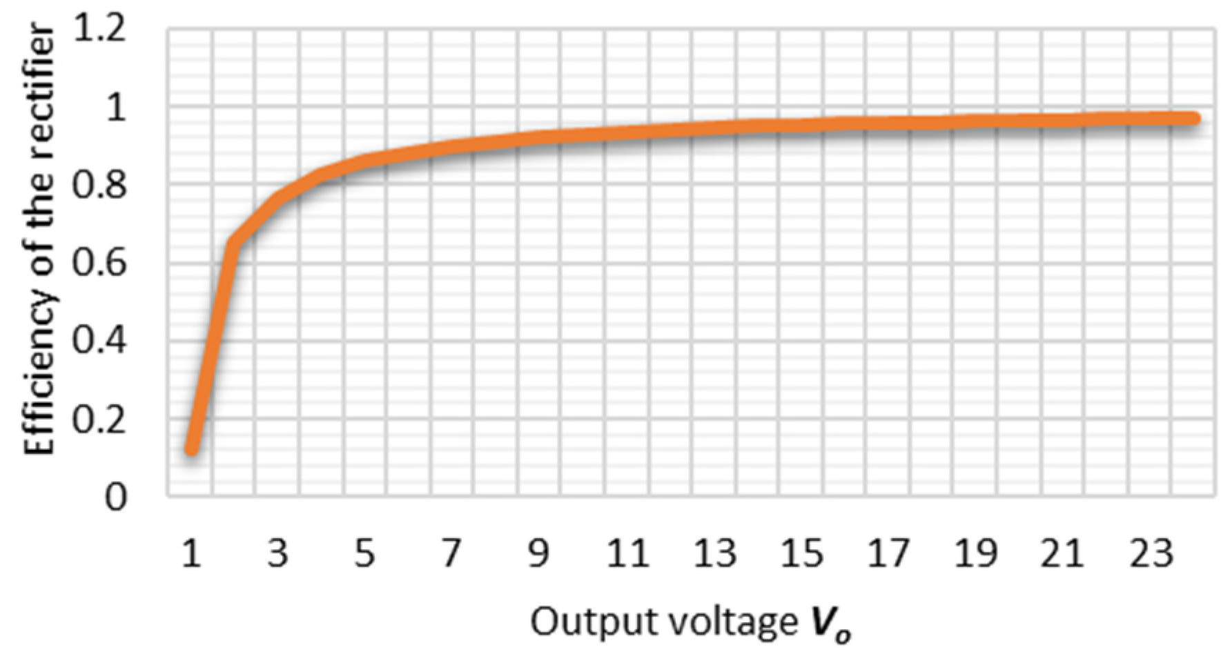
This equation is plotted in Figure 8 assuming a forward voltage in the diodes Vf = 0.7 V. As can be seen in this figure, for an output voltage below 12 V, the efficiency abruptly decreases, so, to maintain a high efficiency, it is recommended that the output voltage verifies Vo > 12 V.
The rectifier efficiency graph in Figure 8 is presented just to show and clarify that it would work with a certain voltage level due to the efficiency of the rectifier. The graph is obtained from a simplified analysis in [33], which assumes that the efficiency of the rectifier is 100%. For this reason, the verification of this graph in the experimental tests is not necessary.
The next step is to reflect the secondary circuit of the inductive coupling to the primary circuit obtaining the circuit shown in Figure 6b. Afterwards, to obtain the equivalent impedance formed by Lls and Req1 (Zeq), the parallel circuit of both elements is evaluated:
Z e q = j X L m p R e q 1 + j X L l s n 2 j X L m p + R e q 1 + j X L l s n 2
Solving and simplifying Equation (7), the equivalent resistance Req2 (real part of Zeq) and equivalent inductance Leq1 (imaginary part of Zeq) are obtained:
R e q 2 = R e q 1 X L m p 2 n 2 R e q 1 n 2 2 + X L m p + X L 1 s n 2 2
L e q 1 = X L m p X L l s n 2 X L m p + X L l s n 2 + R e q 1 n 2 2 ω o R e q 1 n 2 2 + X L m p + X L l s n 2 2
As can be seen in Figure 6c, the resulting equivalent circuit is a serial circuit composed of three inductances, a capacitor, and an equivalent resistance. Finally, the equivalent inductance Leq2 “seen” by the square input voltage Vin is:
L e q 2 = L c + L l p + L e q 1
The final equivalent series circuit is shown in Figure 6c. This circuit will be in resonance when the following condition is satisfied:
X C p = X L e q 2
where Xcp is the reactance of Cp and XLeq2 is the reactance of the inductance Leq2. Equation (13) can be used to calculate the necessary capacitance value Cp in order to operate the circuit at resonance. The resonance condition is important so the switching losses in the MOSFET M1 and M2 are as small as possible. Capacitance Cp can be calculated with the following expression:
C p = 1 ω o 2 L e q 2
Finally, to obtain the value of the compensation inductor, the following equation can be used:
L c = a L l p + L e q 1
where a is a proposed value, and the higher the value of a, the lower the variation of Leq2. The worst case is when the distance d is large, then Llp + Leq1 ≈ 0, and the relationship m between the worst case of Leq2 and the nominal value of Leq2 is:
m = L e q 2 w L e q 2 n = L c L c + L l p + L e q 1 = a a + 1
% error = ( 1 m ) 100
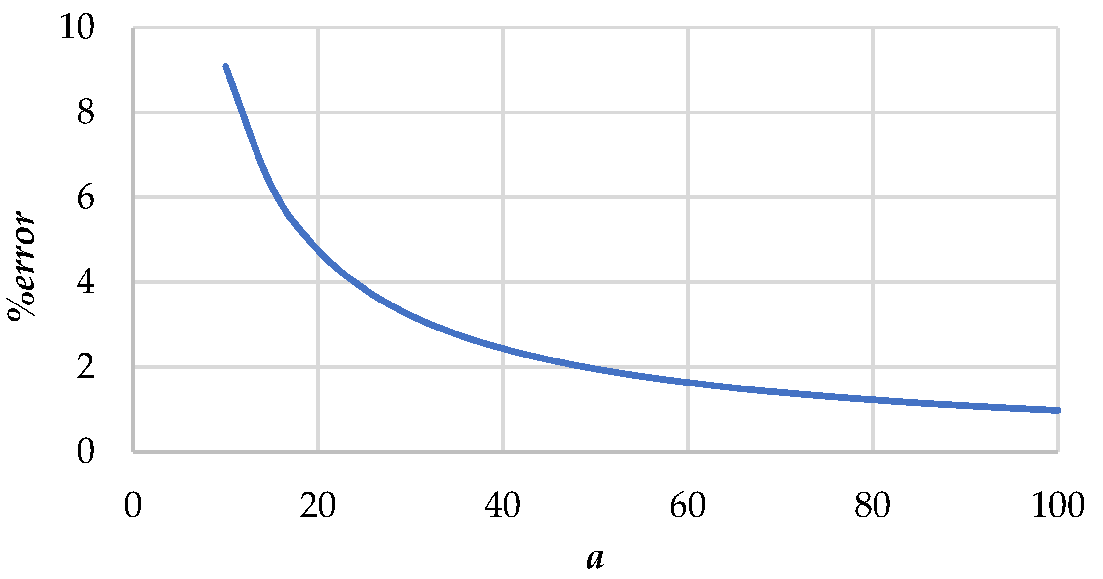
Equation (16) was plotted as shown in Figure 9.
According to Figure 9, the higher the value of a, the lower the percentage of Leq2 variations (%error), so the compensation of the distance d variation in the transmitter and receiver misalignments will be more efficient. For example, for a = 100, the percentage variations of Leq2 (%error) are almost 1, which means no changes in Leq2 for large variations of d.
In this way, it is possible to compensate for the variation in the inductive coupling inductances with respect to the transmission distance and their misalignment. The circuit is expected to remain operating close to the resonance condition so that the maximum energy transfer can be achieved.
To evaluate the performance of the compensation inductor in relation to the resonance and efficiency of the circuit, three values of a will be proposed. The values will be a = 10, a = 20, and a = 30.
The last stage to analyze is the HF inverter, which consists of a half bridge inverter. The RMS current IRMS of the resonant network (when it is operating at resonance) is obtained by applying Ohm’s law using the values of the input voltage Vin and Req2:
I R M S = V i n π R e q 2
Another important characteristic to obtain is the value of average power PM dissipated in each MOSFET of the inverter because this power represents the losses present in the inverter. In this analysis, it is recommended to select a desired dissipated power in the order of mW so that it does not affect the total efficiency of the circuit. Using the IRMS and PM values, the value of Drain-Source ON Resistance RDS(on) that each MOSFET should have is calculated to obtain the estimated losses in the inverter:
R D S ( o n ) = P M I R M S 2
Substituting Equation (16) into (17):
R D S ( o n ) P M R e q 2 2 π 2 V i n 2
Finally, to calculate the total efficiency ɳ value in the proposed IPT circuit, the output power Po (present in the load resistance) and the input power Pin (applied to the HF inverter) are used, which are substituted into the property of P = VI. Then:
η = P o P i n ( 100 % ) = V o I o V i n I i n ( 100 % )

3. Design Methodology

To validate the above equations, a step-by-step design methodology for the resonance condition is proposed in this work. The considered application is to charge smartphones, so the nominal distance between the transmitter and the receiver was d = 1.5 mm.
The design methodology to be shown is when the compensating inductor has a value of 10 times the sum of Llp y Leq1 (a = 10). The proposed methodology is similar in cases where a = 20 or a = 30, and only the values of Lc, Cp and Q change, respectively, in each case.
Table 3 shows the design specifications, and a power of 10 W was considered for wireless chargers for smartphones and the output voltage of 12 V was selected according to Figure 8. The input voltage is considered from a small photovoltaic panel.
The design obtains the properties of the inductive coupling using the following procedure:
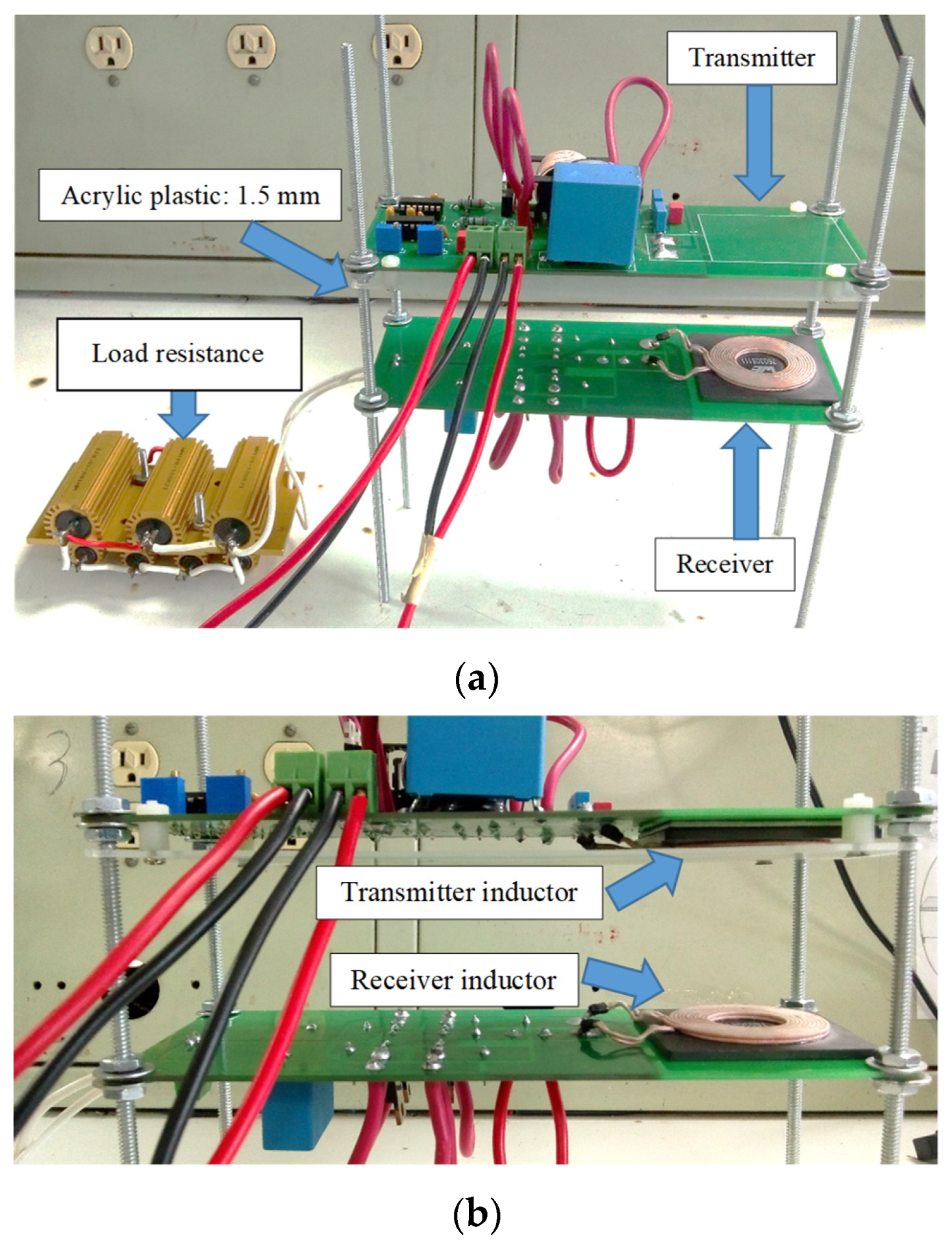
  • Coupling the inductor Lp (transmitter) and Ls (receiver), correctly aligned using an acrylic plastic as the core, the thickness of the acrylic is 1.5 mm; this distance will be the transmission distance d. The inductors should not be connected to any power source or any electrical load during this measurement process.
  • When the inductors are coupled, an LCR tester will be used. A Hioki model 3532-50 was used in this work which is set to measure inductance at a frequency of 500 kHz; this value will be the resonance frequency at which the circuit will operate. The inductance of the primary inductor Lp (primary self-inductance) is measured by the LCR tester. Then, the inductance of the secondary inductor Ls (secondary self-inductance) is measured.
  • Maintaining the same conditions in the inductive coupling, the inductors Lp and Ls are connected in series, and then the measurement of the total series inductance LT is performed with the LCR tester.
  • Using the values obtained in the measurements, the value of the mutual inductance M is calculated:
    M = L T L p L s 2
  • The value of the coupling coefficient k is calculated by substituting the values of Lp, Ls and M into Equation (1).
  • The primary magnetizing inductance Lmp, primary leakage inductance Llp and secondary leakage inductance Lls are calculated, and the values of these inductances are obtained using the equations presented in Table 2.
Using the method described above, the value of the inductive coupling properties shown in Table 4 can be calculated, and then the value of the IPT circuit components can be calculated using the design methodology described in Table 5.
Table 4 presents the characteristics of the wireless transmitter and receiver, the IPT inductors were model WE760308111 from Würth Electronics.
Table 5 presents the design methodology, where the nominal distance d = 1.5 mm, which is the thickness of the acrylic between the transmitter and the receiver.
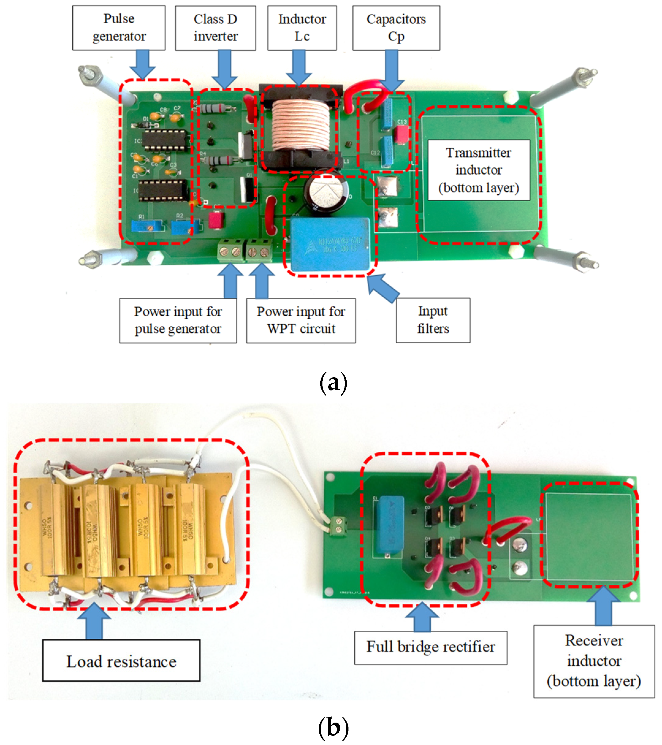
For the implementation of the full bridge rectifier located in the receiver circuit, the MUR840 diodes were selected. This diode model supports an average current of 8A.
The MOSFET IRFZ46N was selected for the high-frequency inverter located in the transmitter circuit. This MOSFET model has an RDS(on) of 16.5 mΩ

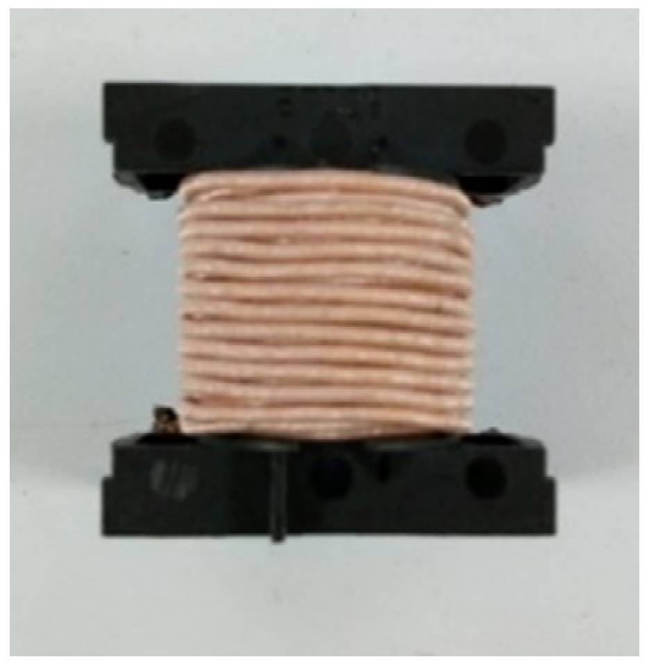
3.1. Implementation of Compensation Inductor Lc

The compensation inductor used for the TPI circuit was manufactured with Litz wire, which is composed of a wire number Nw of 160 wires and each copper wire is 44 AWG. The length of the conductor lc is 3.56 m. The compensation inductor is made up of 63 turns, using an ETD29 model that is shown in Figure 10.
The compensation inductor designed for the TPI circuit has an air core, so the only losses that occur in the component are conduction losses in the copper of the inductor. The copper presents a parasitic resistance that will oppose the flow of electric current through the inductor. Equation (21) presents the formula to obtain the parasitic resistance of the inductor RLc.
R L c = ρ c u l c N w A c
where ρcu is the copper resistivity (17.2 × 10⁻⁹ Ω∙m), lc is the length of the conductor (3.56 m), Nw is the wire number (160 wires) and Ac is the wire cross sectional area (2.463 × 10⁻⁹ m2). Substituting these values into Equation (21):
R L c = ( 17.2 × 10 9   Ω m ) ( 3.56   m ) ( 160 ) ( 2.463 × 10 9   m 2 ) = 155.37   m Ω

3.2. Determination of the Properties of the Inductive Coupling with Different Distances d

In the design methodology, the value of the IPT circuit components was obtained to work correctly at distance d = 1.5 mm. As the circuit is oriented to wireless charging applications of smartphones, it is important to consider that during wireless charging there may be changes in the transmission distance with different causes; these changes directly affect the properties of the inductive coupling, modifying their value.
For that reason, before starting with the implementation of the designed circuit, the measurement and calculation of the inductive coupling properties at different distances d must be performed using the procedure shown at the beginning of Section 3. In the procedure, it is established that the transmission inductors during the measurements should not be connected to any power supply or any electrical load; for this reason, the measurements of the inductive coupling should be performed before the assembly of the IPT circuit on the PCB.
Ten transmission distances were selected as test points to perform measurements of the inductive coupling, with the objective of watching the changes in the coupling with respect to the distance d. This circuit being of the near-field WTP type, the inductor Ls will be moving away from Lp and the plastic acrylic (coupling core) from a distance of 1.5 mm to 4 mm; therefore, there will be 11 measured values for each property of the inductive coupling. The measured and calculated values at each transmission distance are Lp, Ls, LT, M and k.
The LCR tester was used to measure the inductances, while a digital Vernier was used for the transmission distances d. The measured and calculated results are presented in Table 6.

4. Experimental Results

A prototype was implemented to experimentally test the circuit in Figure 5 to validate the design methodology shown in Table 5. Figure 11 and Figure 12 show the implementation of the inductive IPT circuit.
To validate the design conditions, the prototype was adjusted with an initial transmission distance of 1.5 mm. Experimental results are shown in Figure 13. Figure 13a shows the output voltage, output current, and output power. Figure 13b shows the input voltage, input current and input power. The measured values are shown in Table 7, which comply with the design parameters established in Table 3.
The input voltage was adjusted to deliver the nominal voltage to the load. Figure 13c shows the square voltage applied to the resonant tank and the current in the compensation inductor. As can be seen in this figure, the current is in phase with the voltage; therefore, the circuit is in resonance. These results validate the proposed design methodology since they are very similar to the theoretical ones.
The total efficiency ɳ of the IPT circuit is calculated using Equation (19) and the values obtained in the measurements of Pin and Po, which are presented in Figure 13a,b.
η = 10.59   W 14.10   W ( 100 % ) = 75.10 %

Experimental Results with Different Distances “d”

To test the robustness of the circuit for changes in the transmission distance. Ten different test points were performed from 1.5 mm to 4 mm. The following variables were measured: output voltage (Vo), output power (Po), input power (Pin), total efficiency (ɳ) and phase offset (ɸ). The experimental results obtained were compared with the k values obtained in Section 3.2, and the values together are shown in Table 8.
Using the same design methodology already shown, the value of the compensation inductor Lc is calculated. The value of Lc is obtained using Equation (14) when it is 20 (a = 20) and 30 (a = 30) times the sum of Llp y Leq1. The calculation of Lc and Cp when a = 20 is shown in Table 9, while the a = 30 calculation is shown in Table 10.
These new values of Lc and Cp were implemented in the IPT circuit for each case, and experimental tests were performed at different transmission distances using the same method as the tests shown in Table 8. The results are shown in Table 11 and Table 12.
Analyzing the results obtained in Table 7, we can see that the coupling coefficient has a value of 0.734 for a transmission distance of 4 mm. This table shows the output voltage, which falls to 8.56 V when the transmission distance is 4 mm—more than double the nominal value. The output power in this table falls to 5.62 W for a transmission distance of 4 mm. The input power decreases with the transmission distance until a transmission distance of 4 mm. For d = 4 mm, the phase offset angle (ɸ) increases from zero to 39°. The efficiency falls to 54.29% for d = 4 mm.
Comparing the results obtained in Table 8 with the results of Table 11 and Table 12, it can be observed that the coupling coefficient, the output voltage, the output power, and the phase angle present the same behaviour, slightly changing their values when the transmission distance increases up to 4 mm.
The results obtained in the tables show the following:
  • The output voltage value decreases to 10.97 V, although it stays closer to 12 V, as the value of a increases.
  • The output power value decreases to 9.9 W, staying closer to 10 W, as the value of a increases.
  • The total efficiency at a transmission distance of 1.5 mm decreases minimally as the value of a increases. This is because the value of a increases and the value of the inductor wire resistance increases with it.
  • The 10-phase angle (ϕ) stays closer to resonance as the value of a increases. As the inductor value a increases, it will better compensate for the variations caused by misalignment and transmission distance.
From these results, it is observed that the compensation inductor can compensate for changes at the transmission distance of twice the nominal distance of 1.5 mm, achieving a total efficiency of 75.10%. It is important to clarify that the prototype was designed to operate over a wide range of powers and distances between the transmitter and receiver. A specific design for a fixed distance “d”, optimizing the design of the inductor Lc as well as the selection of the semiconductors, and changing them for SiC or GaN semiconductors, can substantially increase the efficiency.
There is a tradeoff between the size of the inductor Lc and the distance “d”; the greater the distance “d”, the larger the inductor Lc required. However, with a higher switching frequency, an excessively large inductor Lc will not be required.
The main disadvantage of the proposal is that the proposed solution is passive. To compensate better for the misalignment and greater distances between the transmitter and receiver, it is recommended to combine this proposal with others such as closed-loop operation and solutions for better coupling factors.

5. Conclusions

This work introduced a very simple compensation topology that consists of only one inductor useful for resonant IPT circuits operating in an open loop for low-power applications and small transmission distance applications (near-field applications), such as wireless chargers of cell phones. To compensate for changes in the transmission distance and misalignment of the transmitter and receiver, only one compensation inductor is added to the resonant tank.
A sufficiently bigger inductor is chosen to maintain the resonant tank operating near resonance for changes until the nominal transmission distance is doubled. The analysis and design methodology for the inductive coupling was presented to establish the resonance condition. The experimental results validate the proposed design methodology. In addition, they confirm the correct functioning of the circuit.
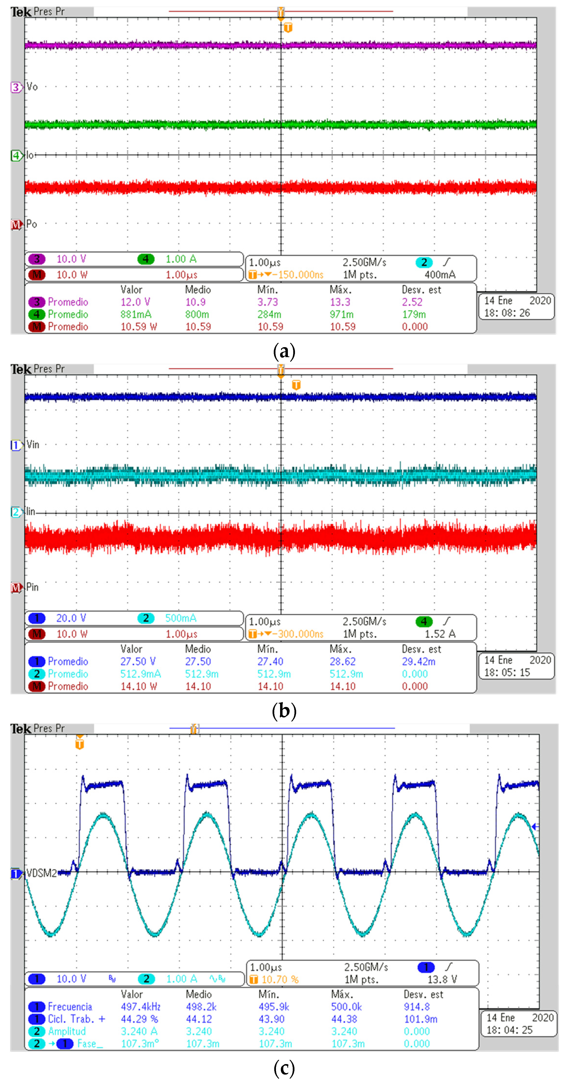
The experimental results obtained under the design conditions validate the proposed design methodology with a maximum error of 5.9% in the output power. A total efficiency of 75% was achieved at a fixed transmission distance of 1.5 mm, using acrylic as a transmission medium.
The implemented circuit operates very near to the resonance condition; comparing the theoretical design values with the experimental results, errors of 0.059% in the phase shift angle and 0.02% in the resonance frequency are obtained.
The results obtained by modifying the transmission distance demonstrate the presence of inductance variations in the inductive coupling as the transmitter inductor moves away from the receiver inductor. However, these variations could be compensated for with only one inductor used instead of more complex compensation topologies. For small variations of the transmission distances (twice or three times), this inductor compensated for the variations in the mutual inductance and self-inductances of the transmitter due to the changes in the coupling factor.
According to the obtained results, the proposed circuit is a good option as a wireless charger for cell phones in which the application transmits power over very short distances.
The circuit proposed in this work is limited to applications where the transmission distance is larger because these applications are of the far-field WPT type. In this type of application, where the distance is large, it would affect the design of the circuit presented in several ways, such as the following:
  • The size of the inductors Lp and Ls would increase considerably in order to realize the wireless power transmission through inductive coupling.
  • The input voltage Vin would need to be increased considerably to compensate for the losses in the inductive coupling, because over long distances, the inductive coupling coefficient k is usually small and the power transmission efficiency from Lp to Ls is low.
  • The size and the value of the compensation inductor Lc would increase because it must compensate for the misalignment of the inductors Lp and Ls in addition to trying to keep the circuit in resonance at a larger transmission distance. As the size of the inductor Lc increases, the series parasitic resistance RLc in the inductor also increases due to the length of the copper conductor, presenting a higher amount of losses in the IPT circuit.
  • As the value of the inductor Lc increases, as a consequence, the value of the primary capacitor Cp will decrease considerably, achieving a value that is difficult to implement because it will be valued in the order of pF or less.
  • The total efficiency will be low due to the losses present in the inductive coupling. In this type of application, it is recommended to combine the circuit proposed in this work with a closed-loop method that allows to adjust the resonance and bring the maximum power transfer from Lp to Ls.
The IPT circuit proposed in this work was validated and works adequately inside the limits previously described; therefore, it is recommended to be used in near-field WPT-type applications and for low-power electronic devices.

6. Discussion

This section will present an in-depth analysis of the results obtained, some of which were not mentioned in the previous sections, as well as some general characteristics, recommendations, contributions of this work, and possible future works to give continuity to the presented topic.

6.1. Relevant Conclusions

Once the work developed in this paper is completed, the following conclusions can be drawn:
  • The resonant network suitable for low-power inductive IPT applications is the series-series topology with inductive coupling; due to this resonant network, operating in resonance has a unity voltage gain. For this reason, the series–series topology was selected for the IPT circuit designed.
  • An analysis and design methodology was developed for the proposed resonant network, which will allow the proposed IPT circuit to operate according to the desired design specifications.
  • The experimental results obtained validate the analysis and design methodology proposed in this work.
  • The implemented IPT circuit enables wireless power transmission from a DC voltage source to an electrical load using resonant inductive coupling to perform the transmission.

6.2. General Characteristics of the Implemented IPT Circuit

The IPT circuit implemented in this work has the following characteristics:
  • The implemented IPT circuit works according to the desired design specifications: 12 volts at the output, 10 watts at the output, the resonant network is in resonance, and the circuit performs the wireless power transmission.
  • The IPT circuit achieves a total efficiency of 75.10% under the design conditions (stationary distance, transmission medium: plastic acrylic of 1.5 mm thickness).
  • It is an easy-to-implement circuit because it operates in an open loop.
  • The prototype is suitable for inductive wireless charging applications, as long as low-power applications are no greater than 10 W.
  • The IPT circuit allows a horizon of wireless battery-charging applications, such as cell phones, electric toothbrushes, electric shavers, portable hearing aids, and hand lamps, among others.
  • The transmitting inductors do not present a temperature rise because they only provide 10% of the inductive reactance of the resonant network.

6.3. Recommendations

To achieve a successful implementation of the proposed IPT circuit, it is recommended to consider the following:
  • It is important to consider that this circuit is for near-field WPT-type applications, especially for wireless charging of low-power wireless devices.
  • For the selection of the diodes of the full bridge rectifier in the secondary circuit, it is recommended to use ultra-fast diodes that are capable of operating correctly at high switching frequencies.
  • For the implementation of the compensation inductor Lc, it is recommended to use Litz wire because it will reduce the series parasitic resistance RLc of this inductor.
  • The transmission inductors Lp and Ls must be identical in structure, inductance, design and size to achieve an efficient coupling coefficient k. It is recommended to use two inductors of the same model designed for IPT applications.
  • For the selection of the MOSFETs of the high-frequency inverter, it is recommended to use a device with the lowest possible RDS(on) to avoid the highest possible conduction losses in the device.

6.4. Contributions of This Work

The work developed has the following contributions:
  • An analysis methodology is contributed for the resonant network of an inductive IPT circuit, in which all the inductances of the inductive coupling are considered as part of a single resonant tank. The literature uses two independent resonant tanks for the analysis—one in the transmitter circuit and one in the receiver circuit.
  • A resonant network topology used for inductive IPT is presented, where a single capacitor is used, which is different from the literature, where two are used (one in the transmitter and one in the receiver); in addition, a compensation inductor is used that contributes 90% of the inductive reactance in the resonant condition [34].
  • A prototype for inductive IPT that is capable of performing wireless power transmission is provided. Such a device is useful in wireless battery-charging applications for low power.

6.5. Possible Future Work

Considering the importance of the resonance and coupling coefficient of the IPT circuit together with the experience obtained in this work, the following recommendations are presented for possible future work:
  • To apply a PLL control loop that allows maintaining the resonance of the resonant network under variations in the inductive coupling. Such variations can be caused by the temperature, the misalignment of the transmission inductors or the transmission distance between both inductors.
  • To use a control technique with active diodes in the rectification stage, which is located in the receiver device, in order to improve the efficiency of the rectifier and consequently the total efficiency of the IPT circuit.
  • Investigate and apply techniques that improve the inductive coupling coefficient in order to improve the efficiency of wireless power transmission. The techniques can be related to the geometry of the transmitting inductors and the use of multiple transmitting inductors.
  • In order to improve the inductive coupling coefficient, the resonant network can be used as an analogue frequency multiplier. The resonant network receives at the input the switching frequency of the inverter, and then a sinusoidal signal with a frequency multiplied “n” times the switching frequency can be delivered to the output. The signal delivered at the output will be the resonant frequency of the resonant network. This method is presented in [4].
These proposals are suggested to give continuity to this work.

Author Contributions

Conceptualization, M.P.-S., A.R.G.-G. and J.A.; Data curation, J.A., J.L.-R. and C.C.-G.; Formal analysis, M.P.-S., A.R.G.-G., J.L.-R. and C.C.-G.; Funding acquisition, M.P.-S., A.R.G.-G. and J.L.-R.; Investigation, M.P.-S., A.R.G.-G., J.A. and C.C.-G.; Methodology, M.P.-S., A.R.G.-G., J.A. and J.L.-R.; Project administration, M.P.-S. and C.C.-G.; Resources, J.A., J.L.-R. and C.C.-G.; Software, A.R.G.-G., J.L.-R. and C.C.-G.; Supervision, M.P.-S., J.A. and C.C.-G.; Validation, J.A., J.L.-R. and C.C.-G.; Visualization, J.A. and C.C.-G.; Writing—original draft, M.P.-S.; Writing—review and editing, M.P.-S., A.R.G.-G., J.A. and J.L.-R. All authors have read and agreed to the published version of the manuscript.

Funding

This research received no external funding.

Data Availability Statement

Not applicable.

Conflicts of Interest

The authors declare no conflict of interest.

References

  1. Tran, M.T.; Thekkan, S.; Polat, H.; Tran, D.-D.; El Baghdadi, M.; Hegazy, O. Inductive Wireless Power Transfer Systems for Low-Voltage and High-Current Electric Mobility Applications: Review and Design Example. Energies 2023, 16, 2953. [Google Scholar] [CrossRef]
  2. Laha, A.; Kalathy, A.; Pahlevani, M.; Jain, P. A Comprehensive Review on Wireless Power Transfer Systems for Charging Portable Electronics. Eng 2023, 4, 1023–1057. [Google Scholar] [CrossRef]
  3. Zhang, Z.; Pang, H. The Era of Wireless Power Transfer; John Wiley & Sons, Inc.: Hoboken, NJ, USA, 2023. [Google Scholar]
  4. Lara-Reyes, J.; Ponce-Silva, M.; Hernández-González, L.; DeLeón-Aldaco, S.E.; Cortés-García, C.; Ramirez-Hernandez, J. Series RLC Resonant Circuit Used as Frequency Multiplier. Energies 2022, 15, 9334. [Google Scholar] [CrossRef]
  5. Manivannan, B.; Kathirvelu, P.; Balasubramanian, R. A review on wireless charging methods—The prospects for future charging of EV. Renew. Energy Focus 2023, 46, 68–87. [Google Scholar] [CrossRef]
  6. Yoo, J.-S.; Gil, Y.-M.; Ahn, T.-Y. High-Power-Density DC–DC Converter Using a Fixed-Type Wireless Power Transmission Transformer with Ceramic Insulation Layer. Energies 2022, 15, 9006. [Google Scholar] [CrossRef]
  7. Ibrahim, H.H.; Singh, M.J.; Al-Bawri, S.S.; Ibrahim, S.K.; Islam, M.T.; Alzamil, A.; Islam, M.S. Radio frequency energy harvesting technologies: A comprehensive review on designing, methodologies, and potential applications. Sensors 2022, 22, 4144. [Google Scholar] [CrossRef]
  8. Mahesh, M.; Kumar, K.V.; Abebe, M.; Udayakumar, L.; Mathankumar, M. A review on enabling technologies for high power density power electronic applications. Mater. Today Proc. 2021, 46, 3888–3892. [Google Scholar] [CrossRef]
  9. Shakil, S.; Rashid, M.H. The potential impacts of wireless power transfer on the global economy, society, and environment. In Proceedings of the IEEE 14th Power Electronics, Drive Systems, and Technologies Conference (PEDSTC), Babol, Iran, 31 January–2 February 2023; pp. 1–5. [Google Scholar]
  10. Iam, I.-W.; Choi, C.-K.; Lam, C.-S.; Mak, P.-I.; Martins, R.P. A constant-power and optimal-transfer-efficiency wireless inductive power transfer converter for battery charger. IEEE Trans. Ind. Electron. 2023, 71, 450–461. [Google Scholar] [CrossRef]
  11. Okasili, I.; Elkhateb, A.; Littler, T. A Review of Wireless Power Transfer Systems for Electric Vehicle Battery Charging with a Focus on Inductive Coupling. Electronics 2022, 11, 1355. [Google Scholar] [CrossRef]
  12. Wu, M.; Su, L.; Chen, J.; Duan, X.; Wu, D.; Cheng, Y.; Jiang, Y. Development and Prospect of Wireless Power Transfer Technology Used to Power Unmanned Aerial Vehicle. Electronics 2022, 11, 2297. [Google Scholar] [CrossRef]
  13. Lara-Reyes, J.; Ponce-Silva, M.; Cortés-García, C.; Lozoya-Ponce, R.E.; Parrilla-Rubio, S.M.; García-García, A.R. High-Power-Factor LC Series Resonant Converter Operating Off-Resonance with Inductors Elaborated with a Composed Material of Resin/Iron Powder. Electronics 2022, 11, 3761. [Google Scholar] [CrossRef]
  14. Benalia, N.; Laroussi, K.; Benlaloui, I. Improvement of the Magnetic Coupler design for Wireless Inductive Power Transfer. In Proceedings of the IEEE 5th International Conference on Power Electronics and their Applications (ICPEA), Hail, Saudi Arabia, 29–31 March 2022; Volume 1, pp. 1–6. [Google Scholar]
  15. Oshimoto, N.; Sakuma, K.; Sekiya, N. Improvement in Power Transmission Efficiency of Wireless Power Transfer System Using Superconducting Intermediate Coil. IEEE Trans. Appl. Supercond. 2023, 33, 1501004. [Google Scholar] [CrossRef]
  16. Rayan, B.A.; Subramaniam, U.; Balamurugan, S. Wireless Power Transfer in Electric Vehicles: A Review on Compensation Topologies, Coil Structures, and Safety Aspects. Energies 2023, 16, 3084. [Google Scholar] [CrossRef]
  17. Chowdhury, S.A.; Kim, S.; Kim, S.; Moon, J.; Cho, I.; Ahn, D. Automatic Tuning Resonant Capacitor to Fix the Bidirectional Detuning with ZVS in Wireless Power Transfer. IEEE Trans. Ind. Electron. 2023, 1–10. [Google Scholar] [CrossRef]
  18. Brovont, A.D.; Aliprantis, D.; Pekarek, S.D.; Vickers, C.J.; Mehar, V. Magnetic Design for Three-Phase Dynamic Wireless Power Transfer with Constant Output Power. IEEE Trans. Energy Convers. 2023, 38, 1481–1484. [Google Scholar] [CrossRef]
  19. Zhou, Y.; Qiu, M.; Wang, Q.; Ma, Z.; Sun, H.; Zhang, X. Research on Double LCC Compensation Network for Multi-Resonant Point Switching in Underwater Wireless Power Transfer System. Electronics 2023, 12, 2798. [Google Scholar] [CrossRef]
  20. Yoo, J.-S.; Gil, Y.-M.; Ahn, T.-Y. Steady-State Analysis and Optimal Design of an LLC Resonant Converter Considering Internal Loss Resistance. Energies 2022, 15, 8144. [Google Scholar] [CrossRef]
  21. Li, Q.; Duan, S.; Fu, H. Analysis and Design of Single-Ended Resonant Converter for Wireless Power Transfer Systems. Sensors 2022, 22, 5617. [Google Scholar] [CrossRef]
  22. Kamali, R.; Gholamian, S.A.; Abdollahi, S.R. An Investigation on Selecting of Resonant Inverter Topologies for Efficient Wireless Power Transmission. In Proceedings of the IEEE 14th Power Electronics, Drive Systems, and Technologies Conference (PEDSTC), Babol, Iran, 31 January–2 February 2023; pp. 1–6. [Google Scholar]
  23. Feng, H.; Cai, T.; Duan, S.; Zhao, J.; Zhang, X.; Chen, C. An LCC-Compensated Resonant Converter Optimized for Robust Reaction to Large Coupling Variation in Dynamic Wireless Power Transfer. IEEE Trans. Ind. Electron. 2016, 63, 6591–6601. [Google Scholar] [CrossRef]
  24. Dai, X.; Qiu, N. Insensitive design for wireless power transfer system using LLC resonant converter. In Proceedings of the 2016 Progress in Electromagnetic Research Symposium (PIERS), Shanghai, China, 8–11 August 2016; pp. 5193–5198. [Google Scholar]
  25. Jang, Y.; Han, J.-K.; Baek, J.-I.; Moon, G.-W.; Kim, J.-M.; Sohn, H. Novel multi-coil resonator design for wireless power transfer through reinforced concrete structure with rebar array. In Proceedings of the IEEE 3rd International Future Energy Electronics Conference and ECCE Asia (IFEEC 2017-ECCE Asia), Kaohsiung, Taiwan, 3–7 June 2017; pp. 2238–2243. [Google Scholar]
  26. Sun, K.; Wang, J.; Burgos, R.; Boroyevich, D. A series-series-CL resonant converter for wireless power transfer in auxiliary power network. In Proceedings of the IEEE Applied Power Electronics Conference and Exposition (APEC), New Orleans, LA, USA, 15–19 March 2020; pp. 813–818. [Google Scholar]
  27. Aldhaher, S.; Luk, P.C.-K.; Whidborne, J.F. Tuning Class E Inverters Applied in Inductive Links Using Saturable Reactors. IEEE Trans. Power Electron. 2013, 29, 2969–2978. [Google Scholar] [CrossRef]
  28. Iannuzzi, D.; Rubino, L.; Di Noia, L.P.; Rubino, G.; Marino, P. Resonant inductive power transfer for an E-bike charging station. Electr. Power Syst. Res. 2016, 140, 631–642. [Google Scholar] [CrossRef]
  29. Shi, L.; Alou, P.; Oliver, J.A.; Cobos, J.A. A Novel Self-adaptive Wireless Power Transfer System to Cancel the Reactance of the Series Resonant Tank and Deliver More Power. In Proceedings of the IEEE Energy Conversion Congress and Exposition, Baltimore, MD, USA, 29 September–3 October 2019; pp. 4207–4211. [Google Scholar]
  30. Berger, A.; Agostinelli, M.; Vesti, S.; Oliver, J.A.; Cobos, J.A.; Huemer, M. A Wireless Charging System Applying Phase-Shift and Amplitude Control to Maximize Efficiency and Extractable Power. IEEE Trans. Power Electron. 2015, 30, 6338–6348. [Google Scholar] [CrossRef]
  31. Ondin, U.; Balikci, A. A Transformer Design for High-Voltage Application Using LLC Resonant Converter. Energies 2023, 16, 1377. [Google Scholar] [CrossRef]
  32. Yao, W.; Lu, J.; Taghizadeh, F.; Bai, F.; Seagar, A. Integration of SiC Devices and High-Frequency Transformer for High-Power Renewable Energy Applications. Energies 2023, 16, 1538. [Google Scholar] [CrossRef]
  33. Erickson, R.W.; Maksimovic, D. Fundamentals of Power Electronics; Springer Science & Business Media: Berlin/Heidelberg, Germany, 2007; pp. 712–713. [Google Scholar]
  34. García-García, A.R.; Ponce-Silva, M.; Cortés-García, C. Dispositivo para Transmisión de Potencia Inalámbrica—Device for Wireless Power Transmission. Mexico, Patent Application: MX/a/2020/011304, Mexican Institute of Industrial Property. 2020. Available online: https://vidoc.impi.gob.mx/visor?usr=SIGA&texp=SI&tdoc=E&id=MX/a/2020/011304 (accessed on 2 July 2023).
Figure 1. Typical structure of inductive power transmission (IPT) circuit.
Inventions 08 00104 g001
Figure 2. Basic compensation networks. (a) series-series, (b) series-parallel, (c) parallel-series, (d) parallel-parallel.
Inventions 08 00104 g002
Figure 3. Resonance conditions used in the literature for IPT circuits.
Inventions 08 00104 g003
Figure 4. Models of IPT circuits. (a) Typical model using coupling inductors. (b) Model T of the coupled inductors using an ideal transformer, (c) model T with secondary reflected to the primary.
Inventions 08 00104 g004
Figure 5. IPT circuit analyzed.
Inventions 08 00104 g005
Figure 6. Analysis of the IPT circuit to obtain the resonance condition, (a) simplified IPT circuit with the equivalent resistance of the rectifier, (b) circuit obtained by reflecting the circuit secondary to the primary circuit, (c) total series equivalent circuit where the resonance condition is established.
Inventions 08 00104 g006
Figure 7. Assumed waveform at the input of the rectifier.
Inventions 08 00104 g007
Figure 8. Efficiency of the rectifier ηr vs. the output voltage Vo (Vf = 0.7 V).
Inventions 08 00104 g008
Figure 9. Percentage variations of Leq2 (%error) in function the factor a.
Inventions 08 00104 g009
Figure 10. Picture of the compensation inductor LC picture used in the IPT circuit.
Inventions 08 00104 g010
Figure 11. Implementation of the inductive IPT circuit, (a) transmitter device, (b) receiver device.
Inventions 08 00104 g011
Figure 12. Prototype experimental assembly, (a) prototype test bench, (b) view of transmission distance setting (adjustable range from 1.5 mm to 4 mm).
Inventions 08 00104 g012
Figure 13. (a) Channel 3: output voltage Vo, 10 V/div (purple). Channel 4: output current Io, 1 A/div (green). Math Channel: output power Po, 10 W/div (red). (b) Channel 1: input voltage, 20 V/div (navy blue). Channel 2: input current, 500 mA/div (light blue). Math Channel: input power, 10 W/div (red). (c) Channel 1: class D inverter output voltage, 10 V/div (navy blue). Channel 2: resonant network current, 1 A/div (light blue).
Inventions 08 00104 g013
Table 1. Comparison of reported resonant circuits with applications in wireless power transmission.
FrequencyOutput PowerCoupling FactorEfficiencyRef.
140 kHz80 W0.2460.70%[23]
40 kHz45 W0.2570.60%[24]
82.3 kHz10 W0.05950%[25]
1 MHz100 W0.2592%[26]
800 kHz12 W0.156%[27]
450 kHz300 W0.3275%[28]
500 kHz2 W0.0565%[29]
120 kHz10 W0.369%[30]
Table 2. Relationships among the coupling inductances models.
ParameterDescriptionValue
LlpPrimary leakage inductance L l p = L 1 M
LlsSecondary leakage inductance L l s = L 2 M
LmpPrimary magnetizing inductance L m p = n 1 n 2   M = M n
Table 3. Design parameters.
ParameterDescriptionValue
PoAverage output power10 W
VoOutput voltage12 V
VinInput voltage27.5 V
fswSwitching frequency500 kHz
foResonance frequency500 kHz
voOutput voltage ripple5%Vo
aRelationship between Lc and (Llp + Leq1)10
Table 4. Characteristics of the wireless transmitter and receiver.
ParameterDescriptionValue
dTransmitter–receiver distance1.5 mm
Transmission medium thickness (inductive coupling core): acrylic plastic1.5 mm
LpPrimary self-inductance8.625 µH
LsSecondary self-inductance8.700 µH
LTTotal series inductance31.727 µH
LlpPrimary leakage inductance. Measured short-circuiting the receiver and measuring the inductance of the primary with the nominal distance d.1.42 µH
Table 5. Design methodology.
ParameterDescriptionEquationValue
MMutual inductance. L T L p L s 2 7.201 µH
kCoupling coefficient. M L p L s 0.831
LmpPrimary Magnetizing inductance L p L l p 7.201 µH
n’Turns relationship of the ideal transformer n’ = n’2/n’1, the turns n’1 and n’2 represent the cross section of coils L1 and L2 that share the same common flux φM. M L m p 1
LmsSecondary magnetizing inductance. M n 7.201 µH
LlsSecondary leakage inductance. L s L m s 1.50 µH
IoOutput current. P o V o 0.833 A
RLLoad resistance. V o 2 P o 14.4 Ω
CfOutput filter capacitor. V o 2 R L f o Δ v R 3.49 µF
nRectFull bridge rectifier efficiency. 1 2 V f V o 0.89
IDDiode average current I o 2 0.417 A
LcCompensation inductor. a L l p + L e q 1 34.31 µH
CpPrimary capacitor. 1 2 π f o 2 1.1 L c 2.711 nF
QQuality factor X C p R e q 2 18.88
RDS(on)Drain-Source ON Resistance P M R e q 2 2 π 2 V i n 2 ≤20 mΩ
ɳTotal efficiency of the IPT circuit P o P i n ( 100 % ) 75%
Table 6. Obtained values of inductive coupling properties at different transmission distances d.
d (mm)Lp (µH)Ls (µH)LT (µH)M (µH)k
1.58.6258.70031.7277.2010.831
1.88.5588.62431.2887.0530.821
28.3928.46730.5476.8440.812
2.28.2688.34329.9316.6600.802
2.58.1468.20829.3066.4760.792
2.88.0538.09728.7946.3220.783
37.9347.98928.2336.1550.773
3.27.8197.86427.6495.9830.763
3.57.7087.74627.0905.8180.753
3.87.5827.62326.5175.6560.744
47.4967.53126.0555.5140.734
Table 7. Experimental results obtained at nominal conditions.
ParameterDescriptionMeasured Value
PoOutput power10.59 W
VoOutput voltage12 V
IoOutput current0.881 A
VinInput voltage27.5 V
IinInput current0.5129 A
PinInput power14.1 W
ɳTotal circuit efficiency75.10%
foResonance frequency497.4 kHz
ɸPhase offset angle0.1074°
Table 8. Experimental results obtained by modifying the transmission distance from 1.5 mm to 4 mm (a = 10).
d (mm)kVo (V)Po (W)Pin (W)ɳ (%)ɸ (°)
1.50.83112.0010.5914.1075.100.10
1.80.82111.7110.0713.5174.55−7.74
20.81211.7010.0513.6073.93−14.40
2.20.80211.369.4612.8473.70−16.74
2.50.79211.119.0712.3573.41−17.50
2.80.78310.838.6111.8572.65−18.68
30.77310.578.2111.5870.84−19.44
3.20.76310.347.8511.6167.61−21.61
3.50.75310.147.5411.8463.72−22.15
3.80.7449.977.3012.3159.31−37.46
40.7348.565.6210.3754.29−39.18
Table 9. Calculation of Lc and Cp when a = 20.
ParameterDescriptionEquationValue
LcCompensation inductor. a L l p + L e q 1 68.62 µH
CpPrimary capacitor. 1 2 π f o 2 1.03 L c 1.406 nF
Table 10. Calculation of Lc and Cp when a = 30.
ParameterDescriptionEquationValue
LcCompensation inductor. a L l p + L e q 1 102.93 µH
CpPrimary capacitor. 1 2 π f o 2 1.03 L c 0.952 nF
Table 11. Experimental results obtained when (a = 20).
d (mm)kVo (V)Po (W)Pin (W)ɳ (%)ɸ (°)
1.50.83112.0010.5714.4972.950.15
1.80.82111.8610.3315.2667.67−3.24
20.81211.7510.1415.2166.65−7.02
2.20.80211.549.7815.1464.59−10.44
2.50.79211.389.5115.0863.04−11.98
2.80.78311.169.1414.9561.16−12.96
30.77311.119.0614.9360.70−14.40
3.20.76310.868.6614.8858.19−15.30
3.50.75310.347.8514.0555.89−18.00
3.80.7449.706.9113.4451.43−18.36
40.7349.096.0712.2249.68−21.78
Table 12. Experimental results obtained when (a = 30).
d (mm)kVo (V)Po (W)Pin (W)ɳ (%)ɸ (°)
1.50.83112.0010.6815.1870.400.13
1.80.82111.9810.6415.7167.74−1.31
20.81211.9510.6016.1365.74−3.29
2.20.80211.9310.5516.1665.28−8.87
2.50.79211.8610.5416.7562.90−9.05
2.80.78311.8410.3917.2360.30−10.25
30.77311.7210.3817.3659.81−10.89
3.20.76311.5710.2717.4458.87−11.58
3.50.75311.3810.1717.4158.41−12.53
3.80.74411.1910.0917.2858.40−13.42
40.73410.979.9017.0358.15−15.35
Disclaimer/Publisher’s Note: The statements, opinions and data contained in all publications are solely those of the individual author(s) and contributor(s) and not of MDPI and/or the editor(s). MDPI and/or the editor(s) disclaim responsibility for any injury to people or property resulting from any ideas, methods, instructions or products referred to in the content.

