Article

An In Situ Automated System for Real-Time Monitoring of Failures in Large-Scale Field Emitter Arrays

by
Reza Farsad Asadi
1,*,
Tao Zheng
2,
Menglin Wang
1,
Han Gao
1,
Kenneth Sangston
3 and
Bruce Gnade
4,*
1
Department of Electrical and Computer Engineering, Southern Methodist University, Dallas, TX 75205, USA
2
Coherent Corp., Sherman, TX 75092, USA
3
Department of Mechanical Engineering, Southern Methodist University, Dallas, TX 75205, USA
4
Department of Material Science and Engineering, University of Texas at Dallas, Richardson, TX 75080, USA
*
Authors to whom correspondence should be addressed.
Instruments 2024, 8(4), 44; https://doi.org/10.3390/instruments8040044
Submission received: 26 August 2024 / Revised: 20 September 2024 / Accepted: 30 September 2024 / Published: 6 October 2024

Abstract

:
Nano-scale vacuum transistors (NVCTs) based on field emission have the potential to operate at high frequencies and withstand harsh environments, such as radiation, high temperatures, and high power. However, they have demonstrated instability and failures over time. To achieve high currents from NVCTs, these devices are typically fabricated in large-scale arrays known as field emitter arrays (FEAs), which share a common gate, cathode, and anode. Consequently, the measured currents come from the entire array, providing limited information about the emission characteristics of individual tips. Arrays can exhibit nonuniform emission behavior across the emitting area. A phosphor screen can be used to monitor the emission pattern of the array. Additionally, visible damage can occur on the surface of the FEAs, potentially leading to the destruction of the gate and emitters, causing catastrophic failure of the FEAs. To monitor damage while operating the device, an ITO-coated glass anode, which is electrically conductive and visible-light-transparent, can be used. In this work, a method was developed to automatically monitor the emission pattern of the emitters and the changes in surface morphology while operating the devices and collecting electrical data, providing real-time information on the failure sequence of the FEAs.

1. Introduction

Electron sources based on field emission are used as cathodes in various applications, including scanning electron microscopes (SEMs), X-ray sources, and traveling wave tubes (TWTs). Nano-scale vacuum transistors (NVCTs), which are configured similarly to vacuum tubes, operate in a vacuum channel. In NVCTs, electron extraction from the cathode to the channel occurs through quantum tunneling. The vacuum channel allows electrons to travel ballistically through the channel, avoiding scattering. This is in contrast to conventional transistors and potentially enables higher mobility and higher-frequency operation [1,2]. Additionally, NVCTs can function in harsh environments, such as those with high radiation, high power, and high temperatures [2,3,4,5,6,7,8].
Despite the potential of NVCTs, challenges like reliability and vacuum packaging persist [9]. NVCTs have shown instability and gradual emission current decay over time in a vacuum environment, with the decay rate increasing when exposed to gasses like O2, CO2, and H2O [10,11,12,13]. This emission current degradation in an oxidizing environment is associated with the formation of an oxide and increase in surface work function [14]. Furthermore, sudden failures and drops in current have been observed, possibly as a result of vacuum arcs [15].
The field emission current depends on the electric field and the work function. To achieve the high electric field required for field emission, in the order of 1–10 MV/cm, one effective approach is to use an emitter with a small tip radius, resulting in a high field enhancement factor [16]. The emission current from a sharp tip can be calculated using the Fowler–Nordheim equation, which considers the applied voltage, work function, and tip radius [17]. For emitters to operate at lower voltages, the tip must be extremely sharp, with a radius of <10 nm. Emitters made from materials such as Si, GaN, and Mo have been reported to have tip radii < 10 nm. Due to the limited emitting area of these sharp tips, even with a high current density of 100 A/cm2, the current emitted from a single tip with a nanometer-scale diameter is <10 µA [18]. To achieve higher current levels, emitters are typically arranged in large-scale arrays known as field emitter arrays (FEAs). Arrays made of Si and Mo with 1 million tips have been reported [19].
NVCTs are built in different configurations, with the most common two being vertical and planar. In planar devices, the anode is integrated into the chip [2,20], while in vertical devices, the anode is usually not integrated. However, some vertically aligned FEAs with integrated anodes have been reported [21]. These arrays typically have a common gate, a common cathode, and a common anode. Measuring the electrical properties of the arrays from the three terminals makes it difficult to gain information about individual tips. The arrays can exhibit nonuniform emission, which can be due to extrinsic factors like an uneven gate voltage distribution or intrinsic factors like emitter nonuniformity. For instance, arrays can have a distribution of tip radii [22], and because the current is sensitive to the radius and field enhancement factor, the arrays show nonuniform emission currents.
There are various methods to detect the emission pattern of FEAs. One approach is using scanning anode microscopy (SAM). In this method, a sharp anode attached to a nanopositioner sweeps over the array and provides a high-spatial-resolution emission pattern of the scanning area [23,24]. This technique is typically used to detect nonuniformities in ungated FEAs, with the anode at a relatively higher voltage than the cathode. However, this method can be time-consuming for large-scale arrays because it tests one tip at a time. Another method involves using phosphor materials to determine the emission uniformity of the entire array. Phosphor screen-coated ITO glass has been widely employed for this purpose and in displays based on FEAs [25,26]. In this method, the emission pattern of the entire array can be captured simultaneously, but the spatial resolution of the emission captured by the phosphor screen is less than the SAM. Materials such as ZnS:Ag, Y2SiO5:Ce, and Gd2O2S:Tb have been used for phosphor screens [27]. Additionally, materials like Polymethyl methacrylate (PMMA) have been successfully used to detect the uniformity of CNTs [28].
Research has been carried out based on in situ analysis of NVCTs. Individual CNTs have been characterized in situ using SEM and TEM [28,29]. Additionally, Rughoboor et al. [24] developed a scanning anode imaging system to monitor the emission sites in Si-FEAs. Ko et al. [30] used a phosphor screen to monitor the emission pattern in a gas environment.
This work focuses on designing and building a vacuum system to detect variations in the surface morphology and emission uniformity of large-scale FEAs. The system will aid in studying FEAs and provide more information about their status during testing. Images are captured by a camera, and data collection is synchronized with the electrical measurements of the devices.

2. Materials and Methods

The system was designed for testing large-scale, self-aligned gated Si-FEAs fabricated at the Microsystems Technology Laboratories at MIT [31,32]. The Si-FEAs are fabricated on 6-inch Si wafers and diced into 6 mm × 6 mm dies, which feature multiple arrays of varying sizes, ranging from 1 × 1 to 1000 × 1000 tips. Figure 1a shows a schematic of the Si-FEA. Each array consists of vertically aligned, gated silicon nanowires with a tip radius of 2–8 nm. These nanowires are 8 µm in height, with diameters of 100–200 nm, and are spaced 1 µm apart. They are isolated from one another by a dielectric matrix consisting of SiO2 and Si3N4, while the cathode is separated from the gate by a SiO2 layer. The gate is composed of polycrystalline silicon (poly Si) and is connected to a Ti/Au metal gate and wire-bonding pad. A half-angle emission of <14° has been reported for similar ungated Si emitters [24]. Additional details regarding the fabrication and characterization of the Si-FEAs are provided elsewhere [26,31,32,33]. Each array shares a common gate, and the entire die has a shared cathode, which is connected to the backside of the die. Notably, the die does not have an integrated anode. The die was mounted onto a modified TO-3 package (HDR00320, Spectrum Semiconductor Materials, San Jose, CA, USA) using electrically conductive epoxy, and the gates of the arrays were wire-bonded to the package pins. Figure 1b shows an image of the wire-bonded die attached to the package.
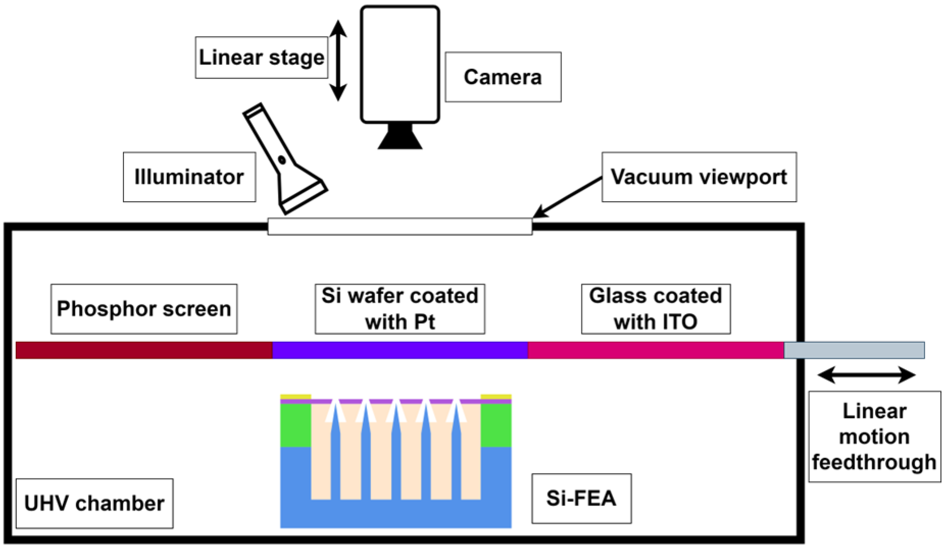
Si-FEAs were tested in an ultrahigh vacuum (UHV) chamber with a base pressure of 6 × 10⁻⁹ Torr. Three different anodes were used in the testing system. One was for detecting the emission pattern of FEAs while testing, and another was used to monitor the changes in the surface morphology of the FEAs during the operation. A P-22 phosphor screen (PHOS-UP22GL-B5X5-R500, Kimball Physics, Wilton, NH, USA) was used to monitor the emission uniformity of the Si-FEAs. To observe any damage on the device’s surface during testing, an electrically conductive and transparent anode was required. Although various transparent conducting films (TCFs) like aluminum-doped zinc oxide (AZO) [34], ultra-thin metal films [35], and graphene [36] are available, indium tin oxide (ITO) is the most common and accessible option [37]. Therefore, a glass substrate coated with ITO was used as a secondary anode. Another anode was a Pt-coated Si wafer. Most of the DC degradation test was conducted with this anode to minimize the exposure time of the phosphor screen and ITO-coated glass to electron emission, thereby avoiding degradation of the phosphor screen [38]. To switch between viewing the emission pattern and inspecting surface damage on the array, the anodes were positioned side by side and moved in front of the FEAs. A schematic of this setup is shown in Figure 2.
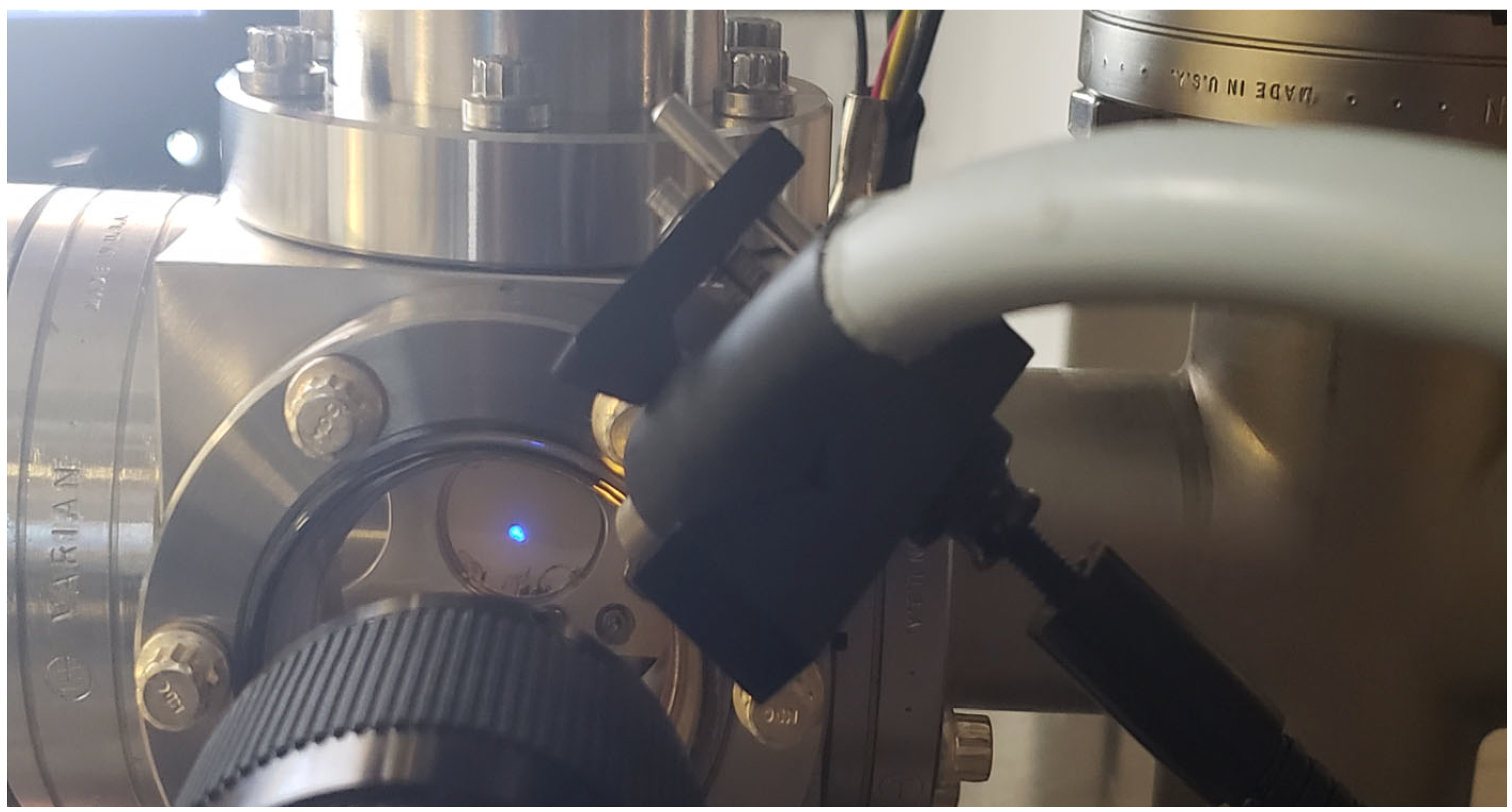
The packaged device was mounted on an adjustable height holder and connected to a DB-9 multipin electrical feedthrough, with the package pins linked to the multipin connectors. The backside of the die connected to the cathode and was electrically connected to the body of the package and the package holder. The package holder was electrically isolated from the chamber using ceramic standoffs. The adjustable height holders allowed for bringing the FEAs to <2 mm from the anodes. This was to ensure clearance of the wire bonds from the anode. A viewport was installed on the opposite side of the chamber to observe the device from outside the vacuum. To minimize the distance between the device under test (DUT) and the camera outside the chamber, a 2.75-inch ConFlat (CF) flange cube was used. As shown in Figure 3, this smaller cube, compared to the commonly used 6-way chambers, resulted in a working distance of less than 2 inches between the DUT and the viewport, allowing for a higher magnification with the same lens and camera. To clean the samples prior to testing, an ultraviolet (UV) lamp (miniZ, RBD Instruments, Bend, OR, USA) was installed on the cube. Research has shown that UV light exposure has a similar effect on desorbing water vapor from FEAs as heating up the sample to 400 °C and can reduce the gate current [39].
To minimize vibration transmission from the pumps to the system, the turbopump (pump: Turbo-V 81-M, Agilent Varian, Palo Alto, CA, USA; controller: Turbo-V 81-AG, Agilent Varian, Palo Alto, CA, USA) was mounted on an optical table using vibration dampers. The turbopump inlet was connected to the cube chamber via a flexible nipple. The chamber was isolated from the table with high-temperature insulating sheets, suitable for baking the chamber. The turbopump was backed by a rotary vane pump (Duo 5 M, Pfeiffer Vacuum, Aßlar, Germany). A glass hot filament ion gauge (Ion gauge: G100F, Kurt J. Lesker, Jefferson Hills, PA, USA; Controller: IG 6600, Kurt J. Lesker, Jefferson Hills, PA, USA) was installed on the chamber to measure the high-vacuum pressure, and a thermocouple gauge (VGT 400, LDS Vacuum, Longwood, FL, USA) was connected to the foreline to monitor the roughing pump pressure. Figure 4 shows a schematic of the test system.
As shown in Figure 4, the phosphor screen was mounted on a holder plate with an attachment to a rod, while a piece of ITO glass was fixed to the plate using BeCu clips. The holder plate was mounted on a linear feedthrough (HLM-275-3, MDC Precision, Hayward, CA, USA) and connected to a stainless steel rod, which held the anode plates. The anode was connected to a MHV feedthrough using a flexible cable to allow for the movement of the linear feedthrough. Ceramic standoffs were used to isolate the rod from the linear feedthrough. This rod was mounted on a UHV-compatible linear bearing and holder, both isolated from the chamber using ceramic standoffs mounted on an adjustable height holder. To compensate for misalignment between the linear bearing and the linear feedthrough, the rod was connected to the feedthrough using a flexible coupling and was electrically isolated with ceramic standoffs. A stepper motor was coupled to the linear feedthrough to allow for automated switching between different anodes.
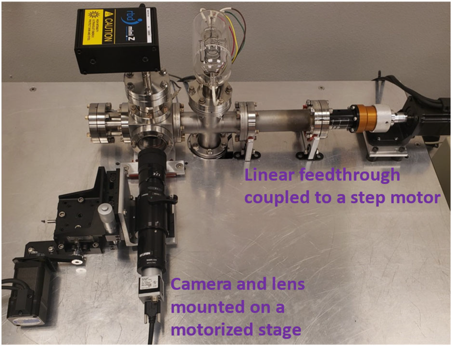
When capturing images of the phosphor screen or the surface of the device, the distances to the camera differed depending on the distance between the device and the screen. To compensate for this change in working distance, the camera (acA1920-150uc, Basler, Ahrensburg, Germany) and lens (MVL12X12Z, Thorlabs, Newton, NJ, USA) were mounted on a multi-axis linear stage to accommodate moving the camera system. A pulley system was mounted on the adjustment shaft of the linear stage and connected to a stepper motor with a controller. Additionally, for capturing better images, the light needs to be on when looking at the device and needs to be off when looking at the phosphor screen. Therefore, a custom-made shutter was placed in front of the illuminator to turn off the light when viewing the phosphor screen and turn it on when viewing the ITO glass. A servo motor was coupled to the shutter to turn the shutter on and off automatically. Figure 5 shows an image of the system containing the stepper motors and stages.
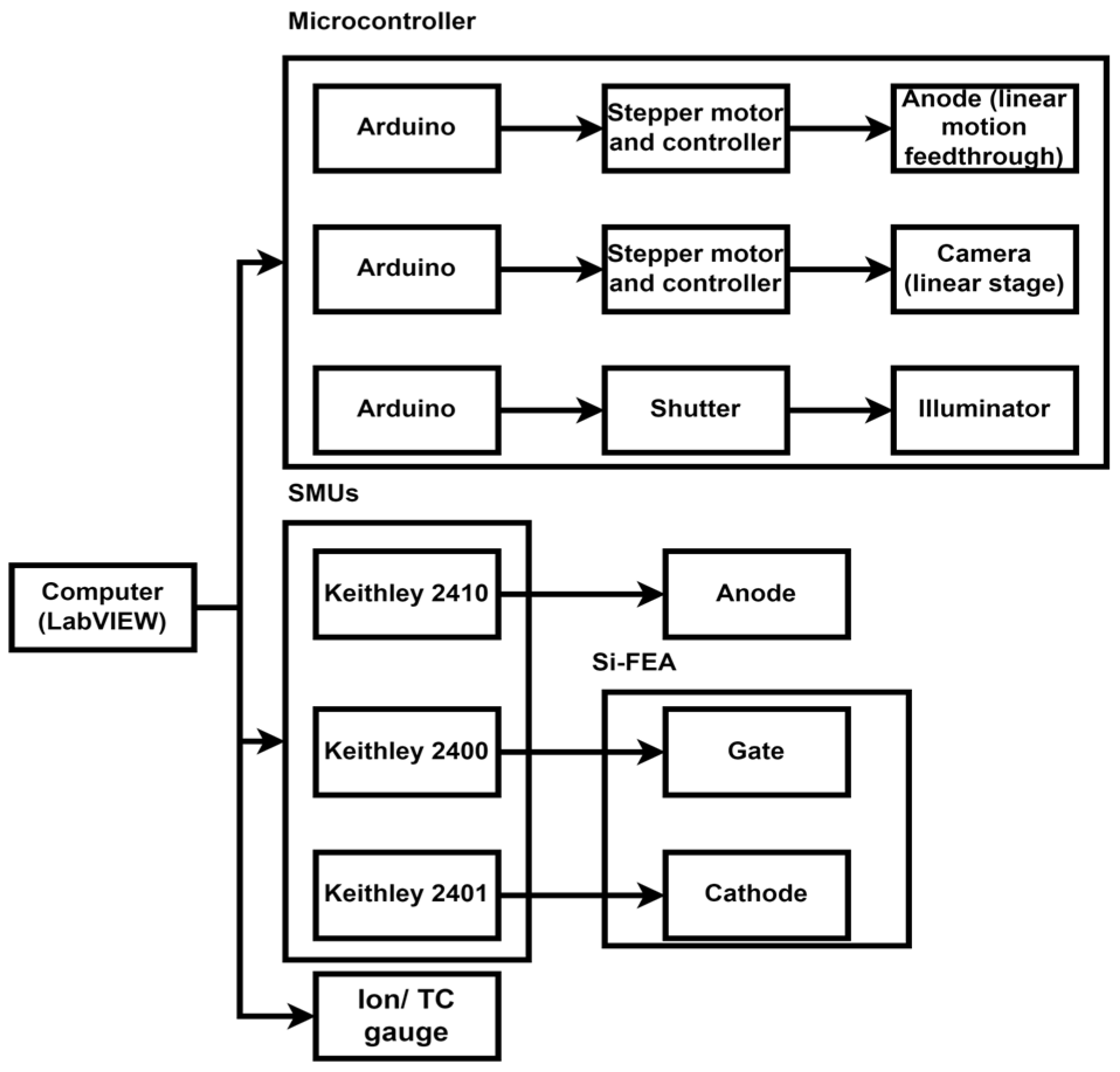
The cathode was connected to a Keithley 2401 SMU and set to 0 V DC, the gate to a Keithley 2400, and the anode to a Keithley 2410 and set to 1000 V DC. These SMUs were interconnected using GPIB cables, connected to the computer via a USB adaptor, and programmed using LabVIEW 2021. The stepper motor controllers were connected to two Arduino microcontrollers, which provided the number of steps and direction of rotation to the controllers. Another microcontroller was used to control the servo motor attached to the illuminator shutter. All three microcontrollers were programmed, connected to a computer via USB cables, and controlled through a LabVIEW interface that managed the stepper motors’ movements and the shutter position. Figure 6 shows a schematic diagram of the system.
As shown in Figure 7, the system has four main states:
  • Retracting the anode to expose the DUT to UV light for desorbing water vapor or for direct observation of the DUT prior to testing (Figure 7a);
  • Using the Pt-coated Si wafer as the anode for the DC degradation experiment (Figure 7b);
  • Monitoring the emission pattern with the phosphor screen in front of the FEAs, the illuminator off, and the camera focused on the phosphor screen (Figure 7c);
  • Monitoring the surface morphology during testing, with the ITO glass in front of the FEAs, the illuminator light on, and the camera focused on the surface of the FEAs (Figure 7d).
The LabVIEW program switches between states 2–4, with the majority of time spent in state 2. Changing the state occurs in parallel with SMU data acquisition and camera imaging.

3. Results

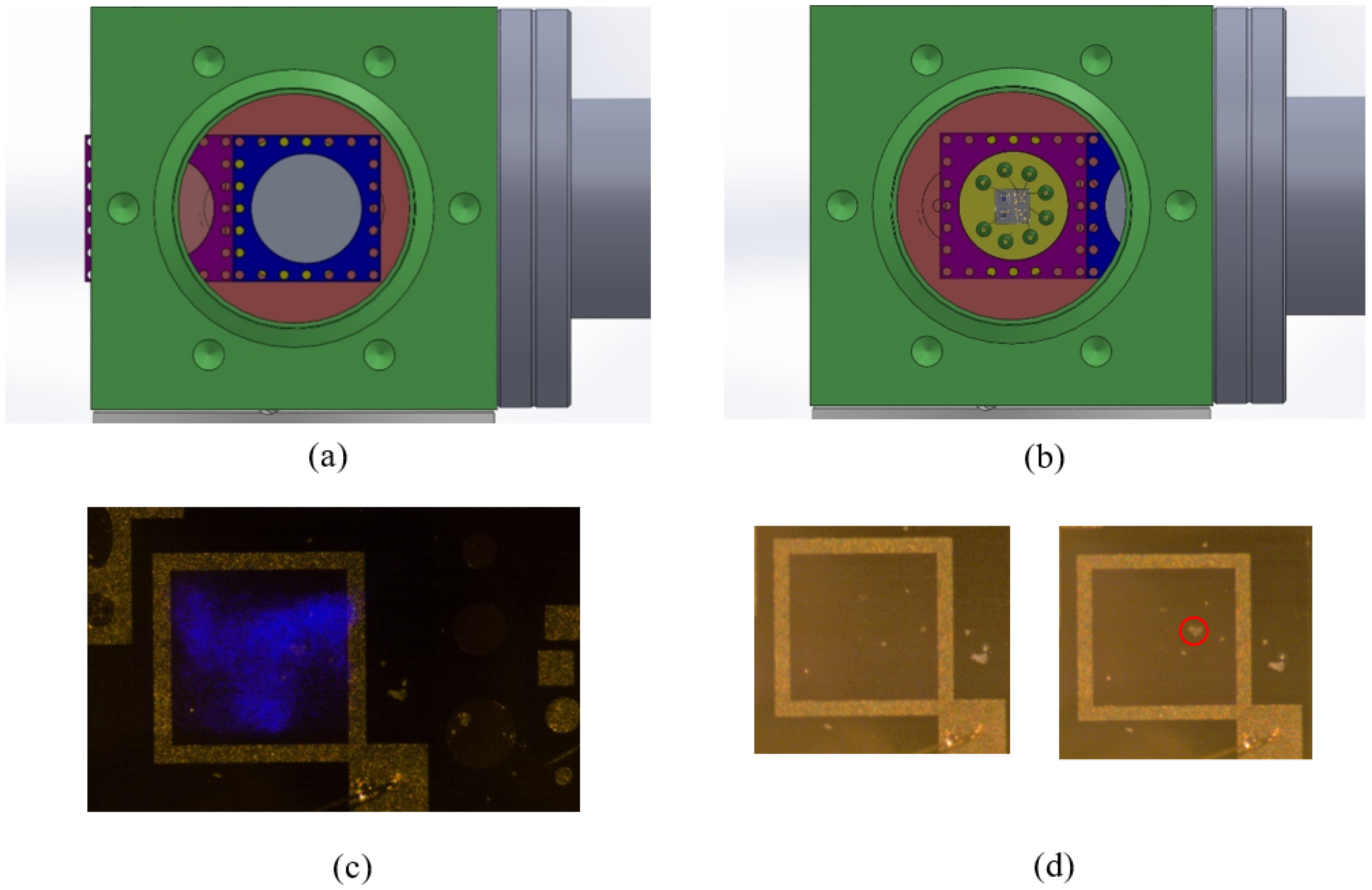
After pumping down and baking out the chamber, the pressure was 6 × 10⁻⁹ Torr. The anode was positioned away from the device. The UV lamp was turned on, and the DUT and chamber were exposed to UV light for 3 h. Multiple I-V sweeps were performed on the device. After the sweeps, the gate voltage was held at 50 V, and the anode voltage was maintained at 1000 V DC throughout the trial. While holding the gate voltage at 50 V DC, the emission pattern was captured using the phosphor screen, as seen in Figure 8, and images of the array’s surface, showing burn spots, were taken, as seen in Figure 9. The anode current also showed an immediate drop when damage spots appeared on the array’s surface.

4. Discussion

In this paper, a system was designed and built to monitor the emission nonuniformity of Si-FEAs and changes in their surface morphology. The system successfully detected the appearance of burn spots on the surface of the FEAs during testing. Changes in the emission pattern, surface morphology, and emission nonuniformity, in correlation with electrical measurement data, can be used to study the failure mechanisms and lifetime of large-scale FEAs in real time.

Author Contributions

Conceptualization, R.F.A. and T.Z.; methodology, R.F.A.; software, R.F.A.; validation, R.F.A., M.W. and H.G.; formal analysis, R.F.A. and T.Z.; investigation, R.F.A.; resources, K.S. and B.G.; data curation, R.F.A.; writing—original draft preparation, R.F.A.; writing—review and editing, T.Z., M.W., H.G., K.S. and B.G.; visualization, R.F.A.; supervision, T.Z.; project administration, B.G.; funding acquisition, B.G. All authors have read and agreed to the published version of the manuscript.

Funding

This research was funded by the Air Force Office of Scientific Research, grant number FA9550-18-1-0436.

Data Availability Statement

The original contributions presented in this study are included in the article, and further inquiries can be directed to the corresponding authors.

Acknowledgments

The authors would like to thank Girish Rughobhoor and Tayo Akinwande for providing the Si-FEAs. Si-FEAs were fabricated at the Microsystems Technology Laboratories at MIT.

Conflicts of Interest

The author Tao Zheng was employed by the company Coherent Corp. The authors declare no conflicts of interest.

References

  1. Tucek, J.C.; Basten, M.A.; Gallagher, D.A.; Kreischer, K.E. Operation of a Compact 1.03 THz Power Amplifier. In Proceedings of the 2016 IEEE International Vacuum Electronics Conference (IVEC), Monterey, CA, USA, 19–21 April 2016; IEEE: Piscataway Township, NJ, USA, 2016; pp. 1–2. [Google Scholar]
  2. Han, J.-W.; Moon, D.-I.; Meyyappan, M. Nanoscale Vacuum Channel Transistor. Nano Lett. 2017, 17, 2146–2151. [Google Scholar] [CrossRef] [PubMed]
  3. Davidson, J.L.; Kang, W.P.; Subramanian, K.; Holmes-Siedle, A.G.; Reed, R.A.; Galloway, K.F. Diamond Vacuum Electronic Device Behavior after High Neutron Fluence Exposure. IEEE Trans. Nucl. Sci. 2009, 56, 2225–2229. [Google Scholar] [CrossRef]
  4. Gotoh, Y.; Morito, T.; Tsuji, H.; Akiyoshi, M.; Nagao, M.; Takagi, I. Robustness of Field Emitter Arrays against High-Energy X-Ray Irradiation at High Dose Rate. In Proceedings of the 2017 30th International Vacuum Nanoelectronics Conference (IVNC), Regensburg, Germany, 10–14 July 2017; IEEE: Piscataway Township, NJ, USA, 2017; pp. 104–105. [Google Scholar]
  5. Morito, T.; Handa, Y.; Gotoh, Y.; Sato, N.; Takagi, I.; Nagao, M.; Akiyoshi, M.; Okamoto, T. Operation of Field Emitter Arrays under High Dose Rate Gamma-Ray Irradiation. In Proceedings of the 2018 31st International Vacuum Nanoelectronics Conference (IVNC), Kyoto, Japan, 9–13 July 2018; IEEE: Piscataway Township, NJ, USA, 2018; pp. 1–2. [Google Scholar]
  6. Singh, A.K.; Shukla, S.K.; Ravi, M.; Barik, R.K. A Review of Electron Emitters for High-Power and High-Frequency Vacuum Electron Devices. IEEE Trans. Plasma Sci. 2020, 48, 3446–3454. [Google Scholar] [CrossRef]
  7. Bhattacharya, R.; Hay, R.; Cannon, M.; Karaulac, N.; Rughoobur, G.; Akinwande, A.I.; Browning, J. Demonstration of a Silicon Gated Field Emitter Array Based Low Frequency Colpitts Oscillator at 400 °C. J. Vac. Sci. Technol. B 2023, 41, 023201. [Google Scholar] [CrossRef]
  8. Sapkota, K.R.; Vizkelethy, G.; Burns, G.R.; Wang, G.T. Effects of Proton Irradiation on GaN Vacuum Electron Nanodiodes. In IEEE Transactions on Electron Devices; IEEE: Piscataway Township, NJ, USA, 2023. [Google Scholar]
  9. Tyler, T.; Shenderova, O.A.; McGuire, G.E. Vacuum Microelectronic Devices and Vacuum Requirements. J. Vac. Sci. Technol. A 2005, 23, 1260–1266. [Google Scholar] [CrossRef]
  10. Chalamala, B.R.; Wallace, R.M.; Gnade, B.E. Poisoning of Spindt-Type Molybdenum Field Emitter Arrays by CO2. J. Vac. Sci. Technol. B Microelectron. Nanometer Struct. Process. Meas. Phenom. 1998, 16, 2866–2870. [Google Scholar] [CrossRef]
  11. Chalamala, B.R.; Wallace, R.M.; Gnade, B.E. Effect of O2 on the Electron Emission Characteristics of Active Molybdenum Field Emission Cathode Arrays. J. Vac. Sci. Technol. B Microelectron. Nanometer Struct. Process. Meas. Phenom. 1998, 16, 2859–2865. [Google Scholar] [CrossRef]
  12. Chalamala, B.R.; Wallace, R.M.; Gnade, B.E. Interaction of H2O with Active Spindt-Type Molybdenum Field Emitter Arrays. J. Vac. Sci. Technol. B Microelectron. Nanometer Struct. Process. Meas. Phenom. 1999, 17, 303–305. [Google Scholar] [CrossRef]
  13. Farsad Asadi, R.; Zheng, T.; Shih, P.-C.; Palacios, T.; Akinwande, A.I.; Gnade, B. Degradation of GaN Field Emitter Arrays Induced by O2 Exposure. J. Vac. Sci. Technol. B 2024, 42, 014001. [Google Scholar] [CrossRef]
  14. Wei, Y.; Chalamala, B.R.; Smith, B.G.; Penn, C.W. Surface Chemical Changes on Field Emitter Arrays Due to Device Aging. J. Vac. Sci. Technol. B Microelectron. Nanometer Struct. Process. Meas. Phenom. 1999, 17, 233–236. [Google Scholar] [CrossRef]
  15. Charbonnier, F. Arcing and Voltage Breakdown in Vacuum Microelectronics Microwave Devices Using Field Emitter Arrays: Causes, Possible Solutions, and Recent Progress. J. Vac. Sci. Technol. B Microelectron. Nanometer Struct. Process. Meas. Phenom. 1998, 16, 880–887. [Google Scholar] [CrossRef]
  16. Urayama, M.; Ise, T.; Maruo, Y.; Kishi, A.; Imamoto, R.I.R.; Takase, T.T.T. Silicon Field Emitter Capable of Low Voltage Emission. Jpn. J. Appl. Phys. 1993, 32, 6293. [Google Scholar] [CrossRef]
  17. Kyritsakis, A.; Xanthakis, J. Derivation of a Generalized Fowler–Nordheim Equation for Nanoscopic Field-Emitters. Proc. R. Soc. A Math. Phys. Eng. Sci. 2015, 471, 20140811. [Google Scholar] [CrossRef]
  18. Guerrera, S.A.; Akinwande, A.I. Silicon Field Emitter Arrays with Current Densities Exceeding 100 A/cm2 at Gate Voltages below 75 V. IEEE Electron Device Lett. 2015, 37, 96–99. [Google Scholar] [CrossRef]
  19. Zhu, N.; Xu, K.; Song, L.; Chen, X.; Chen, J. Fabrication and Characterization of Bulk Molybdenum Field Emission Arrays. In Proceedings of the 2015 Transducers—2015 18th International Conference on Solid-State Sensors, Actuators and Microsystems (TRANSDUCERS), Anchorage, AK, USA, 21–25 June 2015; IEEE: Piscataway Township, NJ, USA, 2015; pp. 1168–1171. [Google Scholar]
  20. Yang, Y.; Turchetti, M.; Vasireddy, P.; Putnam, W.P.; Karnbach, O.; Nardi, A.; Kärtner, F.X.; Berggren, K.K.; Keathley, P.D. Light Phase Detection with On-Chip Petahertz Electronic Networks. Nat. Commun. 2020, 11, 3407. [Google Scholar] [CrossRef] [PubMed]
  21. Shih, P.-C.; Perozek, J.; Akinwande, A.I.; Palacios, T. Anode-Integrated GaN Field Emitter Arrays for Compact Vacuum Transistors. In IEEE Electron Device Letters; IEEE: Piscataway Township, NJ, USA, 2023. [Google Scholar]
  22. Ding, M.; Sha, G.; Akinwande, A.I. Silicon Field Emission Arrays with Atomically Sharp Tips: Turn-on Voltage and the Effect of Tip Radius Distribution. IEEE Trans. Electron Devices 2002, 49, 2333–2342. [Google Scholar] [CrossRef]
  23. Nilsson, L.; Groening, O.; Groening, P.; Kuettel, O.; Schlapbach, L. Characterization of Thin Film Electron Emitters by Scanning Anode Field Emission Microscopy. J. Appl. Phys. 2001, 90, 768–780. [Google Scholar] [CrossRef]
  24. Rughoobur, G.; Ilori, O.O.; Akinwande, A.I. Scanning Anode Field Emission Microscopy of a Single Si Emitter. J. Vac. Sci. Technol. B 2022, 40, 042803. [Google Scholar] [CrossRef]
  25. Spindt, C.A.; Holland, C.E.; Brodie, I.; Mooney, J.B.; Westerberg, E.R. Field-Emitter Arrays to Vacuum Fluorescent Display. IEEE Trans. Electron Devices 1989, 36, 225–228. [Google Scholar] [CrossRef]
  26. Asadi, R.F.; Zheng, T.; Da Silva, J.; Rughoobur, G.; Akinwande, A.I.; Gnade, B. Failure Mode of Si Field Emission Arrays Based on Emission Pattern Analysis. In Proceedings of the 2021 34th International Vacuum Nanoelectronics Conference (IVNC), Lyon, France, 5–9 July 2021; IEEE: Piscataway Township, NJ, USA, 2021; pp. 1–2. [Google Scholar]
  27. Goldburt, E.; Bolchouchine, V.; Levonovitch, B.; Sochtine, N. Highly Efficient Cathodoluminescent Phosphors and Screens for Mid-and High-Voltage Field Emission Displays. J. Vac. Sci. Technol. B Microelectron. Nanometer Struct. Process. Meas. Phenom. 1999, 17, 765–768. [Google Scholar] [CrossRef]
  28. Li, Y.; Sun, Y.; Jaffray, D.A.; Yeow, J.T.W. A Novel Field Emission Microscopy Method to Study Field Emission Characteristics of Freestanding Carbon Nanotube Arrays. Nanotechnology 2017, 28, 155704. [Google Scholar] [CrossRef] [PubMed]
  29. Jin, C.; Wang, J.; Wang, M.; Su, J.; Peng, L.-M. In-Situ Studies of Electron Field Emission of Single Carbon Nanotubes inside the TEM. Carbon 2005, 43, 1026–1031. [Google Scholar] [CrossRef]
  30. Ko, Y.; Jeon, D. Field Emission Influenced by Residual Gas and Passivation of Field Emitters by Diamond Coating. Appl. Surf. Sci. 2003, 215, 228–231. [Google Scholar] [CrossRef]
  31. Guerrera, S.A.; Akinwande, A.I. Nanofabrication of Arrays of Silicon Field Emitters with Vertical Silicon Nanowire Current Limiters and Self-Aligned Gates. Nanotechnology 2016, 27, 295302. [Google Scholar] [CrossRef] [PubMed]
  32. Rughoobur, G.; Sahagún, Á.; Ilori, O.O.; Akinwande, A.I. Nanofabricated Low-Voltage Gated Si Field-Ionization Arrays. IEEE Trans. Electron Devices 2020, 67, 3378–3384. [Google Scholar] [CrossRef]
  33. Zheng, T.; Fasad, R.; Silva, J.; Gnade, B.; Rughoobur, G.; Akinwande, A.I. Failure Mechanism of Large Scale Field Emission Array. In Proceedings of the 2021 22nd International Vacuum Electronics Conference (IVEC), Virtual, 27–30 April 2021; pp. 1–2. [Google Scholar]
  34. Lan, J.-H.; Kanicki, J.; Catalano, A.; Keane, J. An Alternative Transparent Conducting Oxide to ITO for the A-Si: H TFT-LCD Applications. In Proceedings of the Second International Workshop on Active Matrix Liquid Crystal Displays, Bethlehem, PA, USA, 25–26 September 1995; IEEE: Piscataway Township, NJ, USA, 1995; pp. 54–57. [Google Scholar]
  35. Bi, Y.; Liu, Y.; Zhang, X.; Yin, D.; Wang, W.; Feng, J.; Sun, H. Ultrathin Metal Films as the Transparent Electrode in ITO-free Organic Optoelectronic Devices. Adv. Opt. Mater. 2019, 7, 1800778. [Google Scholar] [CrossRef]
  36. Ma, Y.; Zhi, L. Graphene-based Transparent Conductive Films: Material Systems, Preparation and Applications. Small Methods 2019, 3, 1800199. [Google Scholar] [CrossRef]
  37. Qiu, T.; Akinoglu, E.M.; Luo, B.; Konarova, M.; Yun, J.; Gentle, I.R.; Wang, L. Nanosphere Lithography: A Versatile Approach to Develop Transparent Conductive Films for Optoelectronic Applications. Adv. Mater. 2022, 34, 2103842. [Google Scholar] [CrossRef]
  38. Cho, S.H.; Kwon, S.H.; Yoo, J.S.; Oh, C.W.; Lee, J.D.; Hong, K.J.; Kwon, S.J. Cathodoluminescent Characteristics of a Spherical Y2O3: Eu Phosphor Screen for Field Emission Display Application. J. Electrochem. Soc. 2000, 147, 3143. [Google Scholar] [CrossRef]
  39. Bhattacharya, R.; Karaulac, N.; Rughoobur, G.; Chern, W.; Akinwande, A.I.; Browning, J. Ultraviolet Light Stimulated Water Desorption Effect on Emission Performance of Gated Field Emitter Array. J. Vac. Sci. Technol. B 2021, 39, 033201. [Google Scholar] [CrossRef]
  40. Farsad Asadi, R. Empty State Electronics. Ph.D. Thesis, Southern Methodist University, Dallas, TX, USA, 2024. [Google Scholar]
Figure 1. Large-scale, self-aligned gated Si-FEAs [31,32]: (a) Schematic of the Si-FEA showing a current limiter and a tip radius of 2–8 nm. The Si nanowires have a height of 8 µm, a diameter of 100–200 nm, and are spaced 1 µm apart. (b) An image of the Si-FEAs’ die mounted on a modified TO-3 package. The metal package body is electrically connected to the cathode, and arrays of different sizes are wire-bonded to the pins on the package.
Instruments 08 00044 g001
Figure 2. A schematic of the test system in a UHV chamber, featuring the phosphor screen, ITO-coated glass, and Pt-coated Si wafer as anodes.
Instruments 08 00044 g002
Figure 3. An image of the test system from the side showing the chamber and the camera pointing at the DUT. The device is mounted on the flange on the left side and is placed 2 mm from the anode.
Instruments 08 00044 g003
Figure 4. Schematic of the test system showing the UHV chamber with the anodes retracted to view the device using the camera or expose it to UV light: (1) Si-FEA die mounted on a TO-3 package, wire-bonded to the package, and secured to the package holder and DB-9 multipin electrical feedthrough; (2) ITO-coated glass for monitoring surface morphology changes during testing; (3) phosphor screen to monitor the emission pattern; (4) UV lamp to clean the sample before testing; (5) 2.75 in. CF cube; (6) UHV viewport; (7) 2.75 in. CF flexible nipple connecting the chamber to the turbopump; (8) 2.75 in. CF connected to the ion gauge; (9) stainless steel rod for moving the anodes in front of the DUT, connected to a linear motion feedthrough and moving through a linear bearing; (10) MHV electrical feedthrough for supplying voltage to the anode. The CF flange also supports the linear bearing mounted on ceramic standoffs.
Instruments 08 00044 g004
Figure 5. A top view of the test system. The image is adapted from Ref. [40].
Instruments 08 00044 g005
Figure 6. Schematic diagram of the instruments used in the system.
Instruments 08 00044 g006
Figure 7. Images of the four states of the system. The images are adapted from Ref. [40]: (a) retracting the anode for UV exposure; (b) using the Pt-coated Si wafer as the anode; (c) using the ITO-coated glass as the anode; (d) using the phosphor screen as the anode.
Instruments 08 00044 g007
Figure 8. Emission pattern of the Si-FEA displayed on the phosphor screen.
Instruments 08 00044 g008
Figure 9. Schematic of the testing system. The images are adapted from Ref. [40]. The device under test is a 1000 × 1000 Si-FEAs with an active area of 1 mm × 1 mm: (a) looking at the phosphor screen from outside the chamber; (b) looking at the Si-FEAs through the ITO-coated glass; (c) an image of the emission pattern, showing in blue, overlapped with the tested device; and (d) detection of a burnt spot with a <110 µm diameter on the emitting of the array while testing.
Instruments 08 00044 g009
Disclaimer/Publisher’s Note: The statements, opinions and data contained in all publications are solely those of the individual author(s) and contributor(s) and not of MDPI and/or the editor(s). MDPI and/or the editor(s) disclaim responsibility for any injury to people or property resulting from any ideas, methods, instructions or products referred to in the content.