1. Introduction
The development of robust integrated circuits for applications in Nuclear and Subnuclear Physics is a very active field of research. In these applications, normally the on-detector electronics is exposed to ionizing radiation, which limits the usage of commercial off-the-shelf (COTS) components. Radiation-exposed components are usually custom integrated circuits (ASICs) and special technological processes or layout hardening techniques are adopted for them. These devices are usually designed to operate for several years on particle detectors withstanding the expected radiation environment, and they implement various functions including analog and mixed signal conditioning on front-end boards (e.g., [
1,
2]), local trigger logic (e.g., [
3]), and high-speed data transmission (e.g., [
4,
5]) to counting rooms, where no radiation is present. Unfortunately, ASICs become unavailable as soon as the technological process they are fabricated with becomes obsolete. Part of the design effort is portable to newer technologies, mainly the higher levels of design, but each new development requires designing a new device. The fabrication costs can reach up to a few million euros and the development typically requires tens of person-months to design, test and debug. Moreover, even if periodically new efforts are spent to design new devices, and to follow the always-increasing performance demand, obsolescence is destined to recur. For these reasons, much effort is being spent for mitigating ASIC-related obsolescence and design issues, by focusing on COTS reconfigurable devices instead. As far as it concerns purely digital functions, COTS components which are useful for this goal are latest-generation Static RAM-based Field Programmable Gate Arrays (SRAM-based FPGAs) [
6,
7,
8]. They include high-speed serial IOs (up to 32 Gbps), offer wide processing capabilities and are reconfigurable on the field, in real-time. Moreover, with respect to ASICs, FPGAs require a reduced design effort and time. In the case of FPGAs, obsolescence-related issues are reduced since porting a design from an old device to a new one requires mostly logic remapping, which in part can be automatic. Porting does not require the designer to cope with device issues, which are already solved by the FPGA vendor. Today, the scaling of modern technological processes for SRAM-based FPGAs has dramatically increased their total ionizing dose (TID) hardness level. In fact, commercial sub-28 nm CMOS processes–such as the one used for the Xilinx 7-Series or Ultrascale families–can tolerate TID of the order of 1 Grad(Si) [
9]. The TID tolerance of these processes is compatible with requirements for inner trackers [
10] at the High-Luminosity Large Hadron Collider (HL-LHC) at CERN, for instance. However, the use of SRAM-based FPGAs in radiation environments is mostly limited by their sensitivity to radiation-induced upsets [
11,
12] in the configuration memory. Such effects may modify the programmed routing paths and logic elements, altering the intended functionality of the firmware.
Methods based on triple modular redundancy [
13] and periodic correction of the configuration, i.e., configuration scrubbing [
14,
15], are used in order to correct single event upsets (SEUs), which generally become more significant as the technological scaling proceeds towards smaller feature sizes. Recent devices include dedicated self-correction hardware for configuration error detection and correction (EDAC), which can detect and correct nearly 0.1% of the bits at each configuration memory address. Hybrid scrubbing solutions [
16] also exploit external radiation-hardened memories, which preserve a golden copy of the FPGA bitstream, but they make it possible to correct 100% of the frame bits. These additional components increase the overall system complexity, cost and power consumption. Recent developments in configuration scrubbing consist of techniques based on majority-voting of configuration, and they make it possible both to avoid adding external memories and to correct any number of errors.
The contribution of this work to the state of the art is twofold. On the one hand, we describe in detail the architecture of a custom scrubber based on majority-voting and we discuss our implementation choices in a Xilinx 7-Series FPGA. On the other hand, we discuss measurements of the reliability of our solution in a proton irradiation test and we compare it with a scrubber provided by the vendor, i.e., the Xilinx Soft Error Mitigation (SEM) controller.
The rest of this manuscript is organized as follows. In
Section 2, we describe the organization of configuration memory in Xilinx devices. In
Section 3, we briefly introduce the main features of the SEM controller. In
Section 4, we introduce the principles of configuration scrubbing based on majority-voting and comment about some referenced solutions. In
Section 5, we present the architecture of our custom majority-voting-based scrubber. In
Section 6, we discuss the architecture of the serial link which we used as a benchmark design for testing the scrubber repair capability. In
Section 7, we describe the implementation of the whole design combining both the link and the scrubber. In
Section 8, we present the test setup we used for performing irradiation tests. In
Section 9, we describe the test results. In
Section 10, we draw the conclusions.
2. Configuration Memory in Xilinx
FPGAs
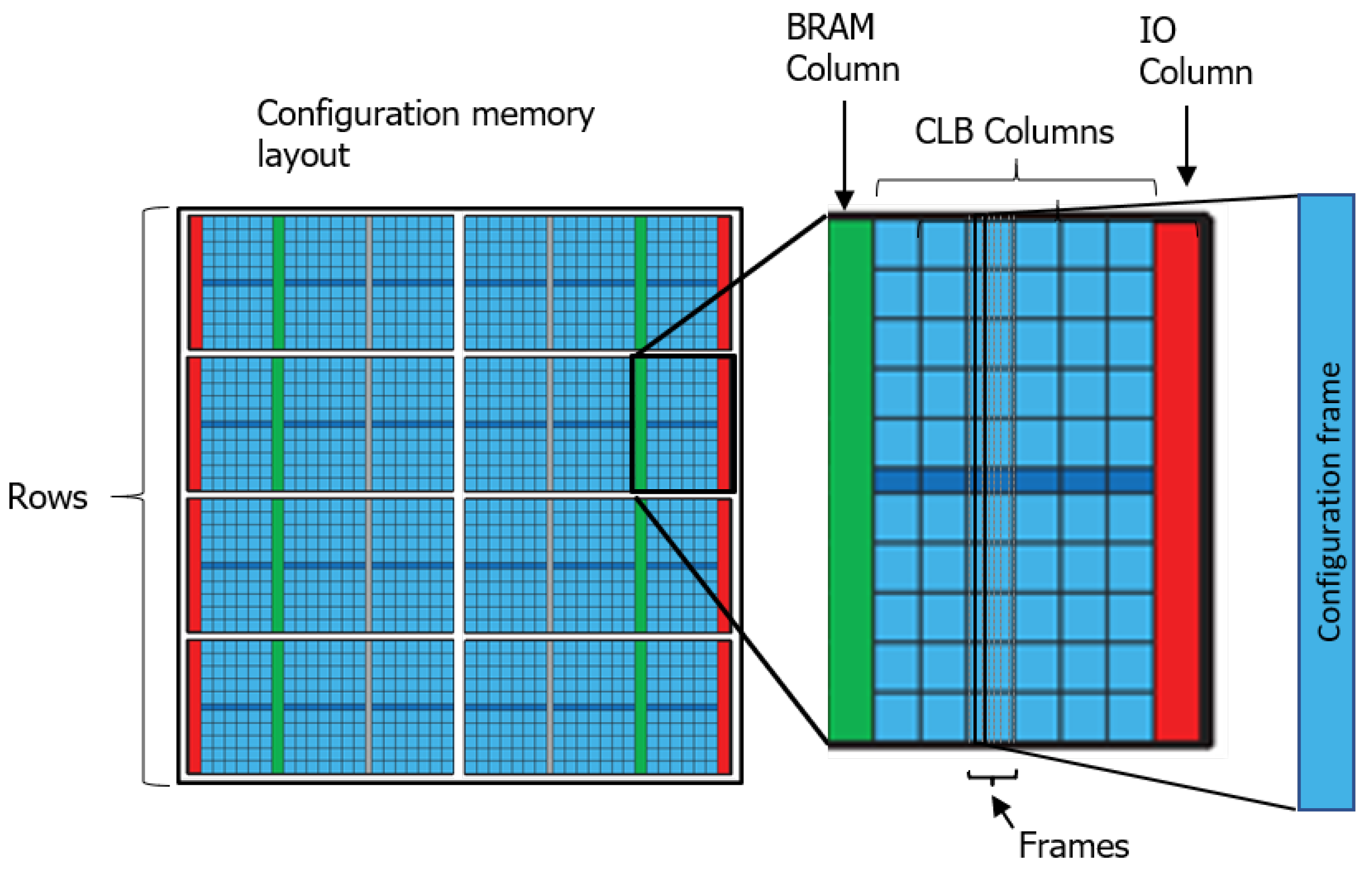
The logic implemented by an FPGA is determined by the so-called “configuration memory”. In Xilinx devices, it consists of static RAM cells, which determine all the programmable features. These include, for instance, routing of internal signals, content of look-up-tables (LUTs), IO voltage levels and drive strengths. From a logical point of view, the memory is divided into rows (
Figure 1). Each row extends over the full width of the device and is partitioned in columns. A column configures a specific hardware resource. For example, a column may configure a slice of programmable routing, LUTs, block RAMs, etc. Each column is partitioned in a certain number of frames, and this number varies with the type of the hardware resource. In modern devices, a frame includes normally thousands of bits (e.g., 3232 in Kintex-7 family and 3936 in Ultrascale).
3. The Soft-Error Mitigation Controller
The SEM [
17] controller is a soft-core provided by Xilinx for detecting and correcting soft errors in the configuration memory. The features of the SEM depend on user options and on the specific FPGA family, thus we discuss those for the Xilinx 7-Series, which is relevant to this work. The SEM is capable of optional error correction using three different methods: repair, enhanced repair, or replace. The repair method is based on error correcting codes (ECCs) embedded in configuration frames as extra bits added to the actual configuration data. With this method, the SEM can correct 1 bit per frame. The enhanced repair method combines ECCs and a hardware cyclic redundancy check (CRC) and it makes it possible to correct up to 2 bits per frame. The replace method reloads corrupted configuration frames from an external golden memory, which is assumed not to fail. For example, it could be radiation-hardened or it could be sitting out of the radiation environment. This method makes possible to correct any number of bits per frame. The controller has a typical detection latency of 25 ms. It supports error injection and error classification by means of the Xilinx Essential Bits (EB) design flow. The EB flow makes it possible to determine whether an upset can potentially affect the design operation or if it can be safely ignored. The operational frequency of the core is limited by the internal configuration access port (ICAP) used for accessing the configuration.
It is worth remarking that the SEM, as well as any other configuration scrubber, operates only on configuration memory. Other storage resources such as block memories, distributed RAM or flip-flops have to be protected at the design level, by means of appropriate techniques, such as triple modular redundancy or error correcting codes.
4. Majority-Voting-Based Configuration Scrubbing
Since the topology of hardware resources in FPGAs is normally quite regular, their layout and therefore the logic structure of the associated configuration memory is regular. Therefore, it is usually possible to find regions with an identical layout which map to identical sequences of columns, thus of frames. In addition, it is important to remind that unprogrammed resources have the pertaining frames set to a default, predictable value, which in Xilinx devices is all bits at “0”. If the FPGA and the given design are such that for any programmed column it is possible to find at least other two identical unprogrammed columns, then any column can be replicated twice. It is therefore possible to majority vote the configuration from the three copies of the column, i.e., the original one pertaining to the design and the two replicas. Majority voting of configuration frames can be performed by means of partial reconfiguration techniques, which allow accessing each frame individually.
When one of the redundant copies is different from the result of the voting, that copy can be replaced with said result. Assuming no errors in homologous bits of redundant frames, this makes it possible to correct the errors in the replaced frame. Techniques based on this concept bring together two key features, which do not normally co-exist in other scrubbing solutions. In fact, on the one hand, they make it possible to correct a significant amount of errors per configuration frame and, on the other hand, the implementation does not require storing the golden configuration data outside the chip. It is possible to envisage different methods for generating the redundant copies. For instance, in [
18], redundant frames are generated by replicating the same layout, and therefore the same configuration, in different identical subsets of the gate array. The redundant layouts are also used to provide redundant functionality and to majority vote the logic outputs in real-time. The technique requires the usage of Xilinx legacy tools and a custom design-flow [
19], which does not support latest generation devices. Moreover, this solution leads to a power consumption increase related to the additional programmable resources used. Another example is given in [
20,
21], where redundant copies are directly generated by reading the configuration data back from frames to be protected and by writing them to other free and compatible ones. The patents in [
22,
23] describe a technique for generating a redundant configuration based on the verification of the copy, the functional testing of the design, and the measurement of the power consumption during redundancy generation. We used this technique for generating the redundant configuration used for majority-voting by scrubbers presented in this work. This experimental approach does not provide triple modular redundancy but it avoids the related additional power consumption. Moreover, it makes it possible to ignore details about the association between configuration bits and hardware resources. On the top of that, it can provide redundant configuration even for resources which are not present in multiple instances in the device. The technique is applicable both to basic blocks such as flip-flops, LUTs and routing, and complex macros such as high-speed IO transceivers, clock management units, digital signal processing blocks, etc.
5. Scrubber Architecture
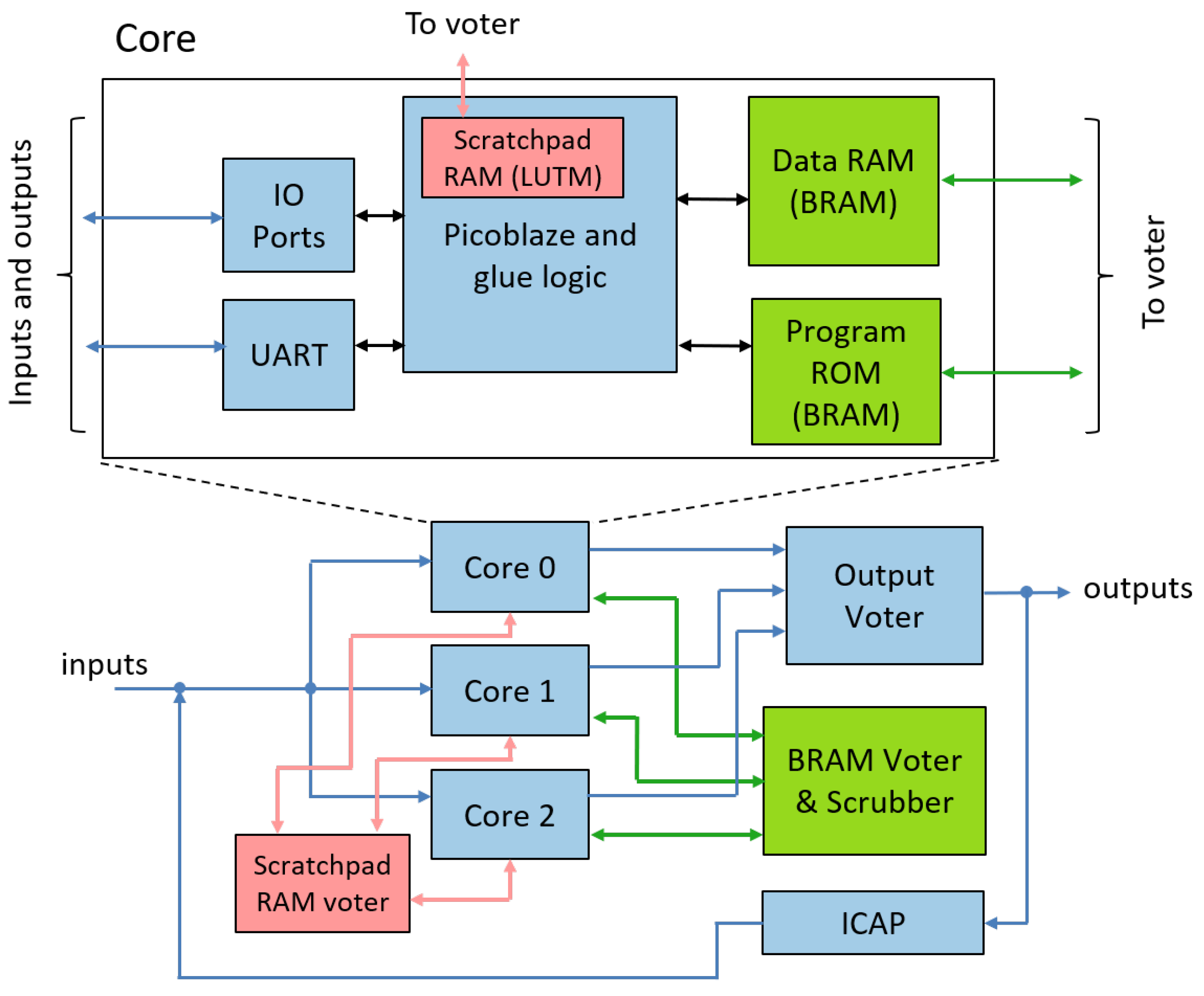
Our configuration scrubbing method is implemented in software and it runs on Picoblaze (PB) [
24], a lightweight 8-bit soft microcontroller provided by Xilinx and supported by most device families. We designed a triple modular system based on PB (
Figure 2). The system includes three cores (Core0, Core1 and Core2). Each core includes a PB, a 4k 18-bit words memory for the program (Program ROM), a 4k 8-bit words memory for data storage (Data RAM) and glue logic for IO (IO ports). The main purpose of the RAM is storing the bits of three frames to be voted, the result of voting and the list of frames to be scrubbed. The Data RAM and the Program ROMs are both dual-port block RAMs. One port is accessed by PB, while the other one is used in background by a dedicated logic to perform a cross majority voting between the RAMs from the three cores. The outputs of IO ports are voted by dedicated hardware and signals to input ports are routed redundantly to each core. All hardware majority voters are in turn tripled and majority-voted. During operation, the PB core is periodically reset for clearing possible upsets in all its registered elements. The period is programmable in terms of the number of frames to be scanned before a reset is asserted and it is specified at run-time. At each reset, the PB internal scratchpad memory (128-byte distributed RAM) and its internal registers (two banks of 16 8-bit registers) are majority-voted in software across the three cores through IO ports. The scrubbing process includes majority voting of redundant frames and forcing unprogrammed frames to remain in their default state (all bits cleared).
The three cores access configuration via the ICAP, which is tied to specific hardware resources to access the configuration and it cannot be tripled due to limitations of the FPGA. The UART serial output is also not tripled as it is used mainly to report upsets detected by the scrubber.
6. Serial Link Node Architecture
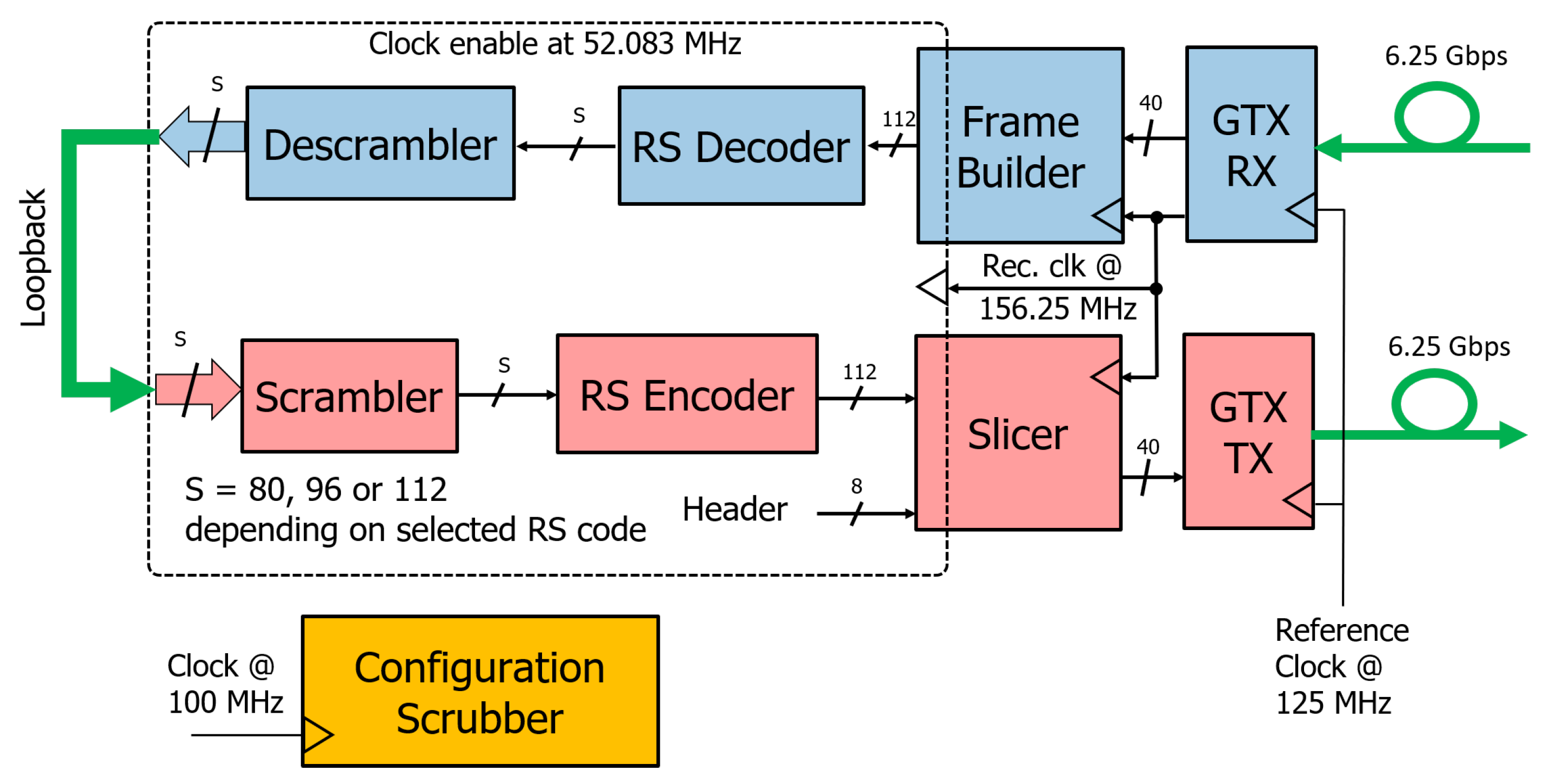
To measure the scrubber impact on the functionality of a design, we designed a high-speed serial link node with a line rate of 6.25 Gbps built around the Xilinx GTX transceiver (
Figure 3). We designed the node having in mind typical applications in HEP experiments, such as clock and trigger distribution and data transfer. The serial link node is aimed at being used on-detector, thus in the presence of radiation. The architecture includes a receiver and a transmitter, and the configuration scrubber. We developed our custom data transfer protocol, which includes scrambling for DC-balance and forward error correction (FEC) based on Reed–Solomon (RS) codes. The protocol also makes it possible to select codes for different data protection levels, at run-time. Data are partitioned in 120-bit frames. Each frame includes an 8-bit header and 112-bit scrambled and RS-protected data. The scrubber is independent by the link node and it operates in background on a clock signal unrelated to the link.
The GTX receiver recovers 40-bit data parallel data from the serial stream and it also recovers a clock at 156.25 MHz, which synchronizes the whole link node. Additional logic in the FPGA fabric operates with a clock enable at 52.083 MHz. It aligns to the correct frame boundary (Frame Builder) and it implements FEC decoding (RS Decoder) and descrambling (Descrambler) to output payloads carried by frames (80, 96 or 112-bit size, depending on the selected RS code). Received payloads are routed back to the link transmitter, which re-scrambles, re-encodes and re-slices data into 40-bit words to feed the GTX transmitter at 156.25 MHz. The whole node is a logical loop-back, thus it makes it possible to measure bit error ratio remotely and to test clock recovery, since the whole node is clocked by the recovered clock.
7. Implementation
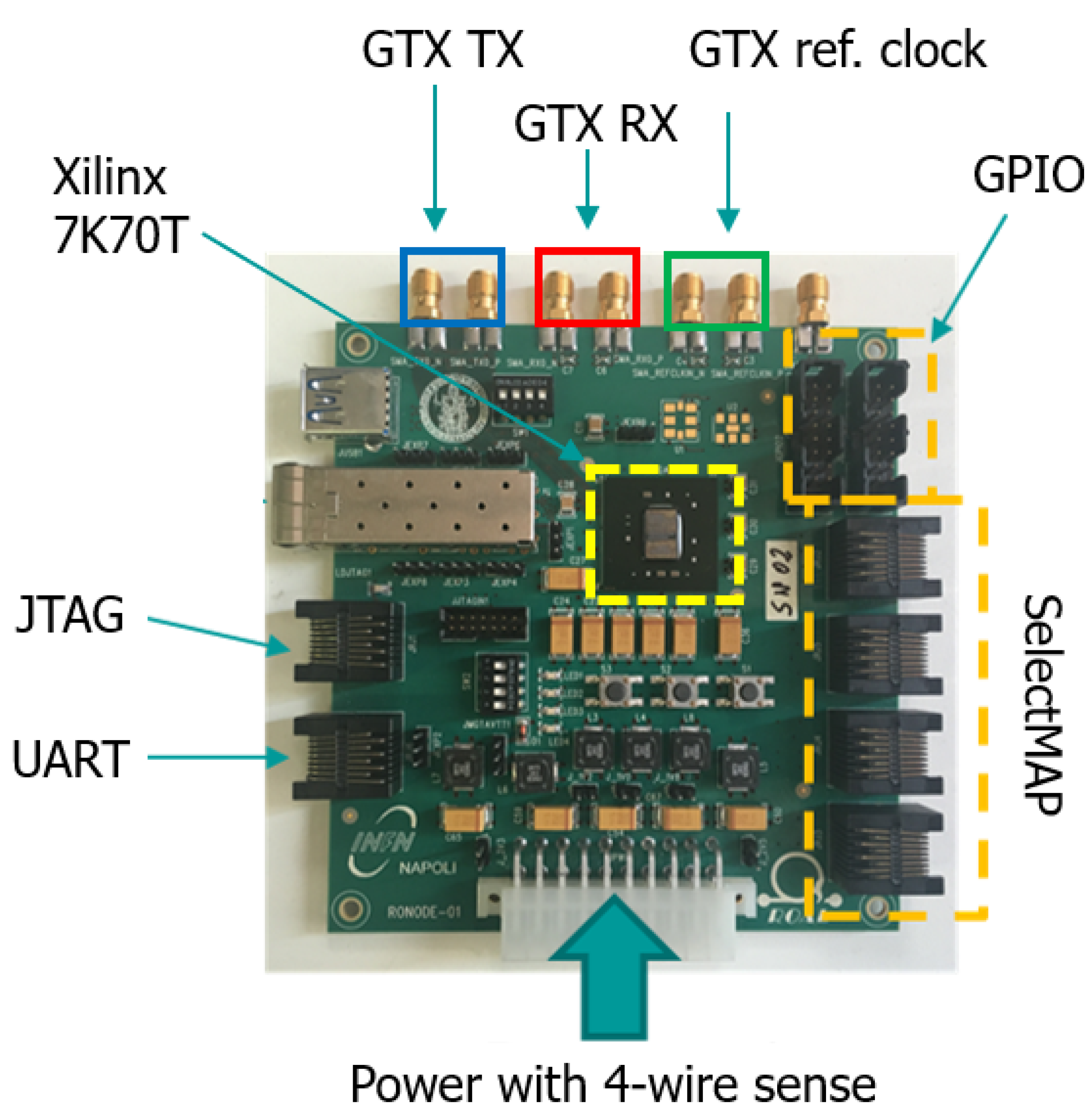
The scrubber implementation was tailored to a custom board designed for radiation testing (
Figure 4). The board is built around a Xilinx 7-Series 70T FPGA [
25]. To avoid failures unrelated to the FPGA, the board does not host any other active component. The power is provided externally in order to be easily measured at the different power domains of the device. A four-wire sensing scheme is adopted for compensating the voltage drop on the power cable.
We implemented the link node in three versions; two were protected by our voting scrubber and one by the Xilinx SEM. The first two versions differ in the clocking scheme for the scrubber. In the first one, the clock signal for the scrubber comes from an external source, while, in the second one, it is generated on-chip by means of digitally-controlled oscillator (DCO) implemented in the FPGA fabric. The DCO is based on the digitally-controlled delay line described in [
26]. This second clocking scheme is aimed at applications in which an additional independent clock for the scrubber is not available. The layouts of the firmwares of the DCO-clocked voting scrubber and of the SEM are shown in
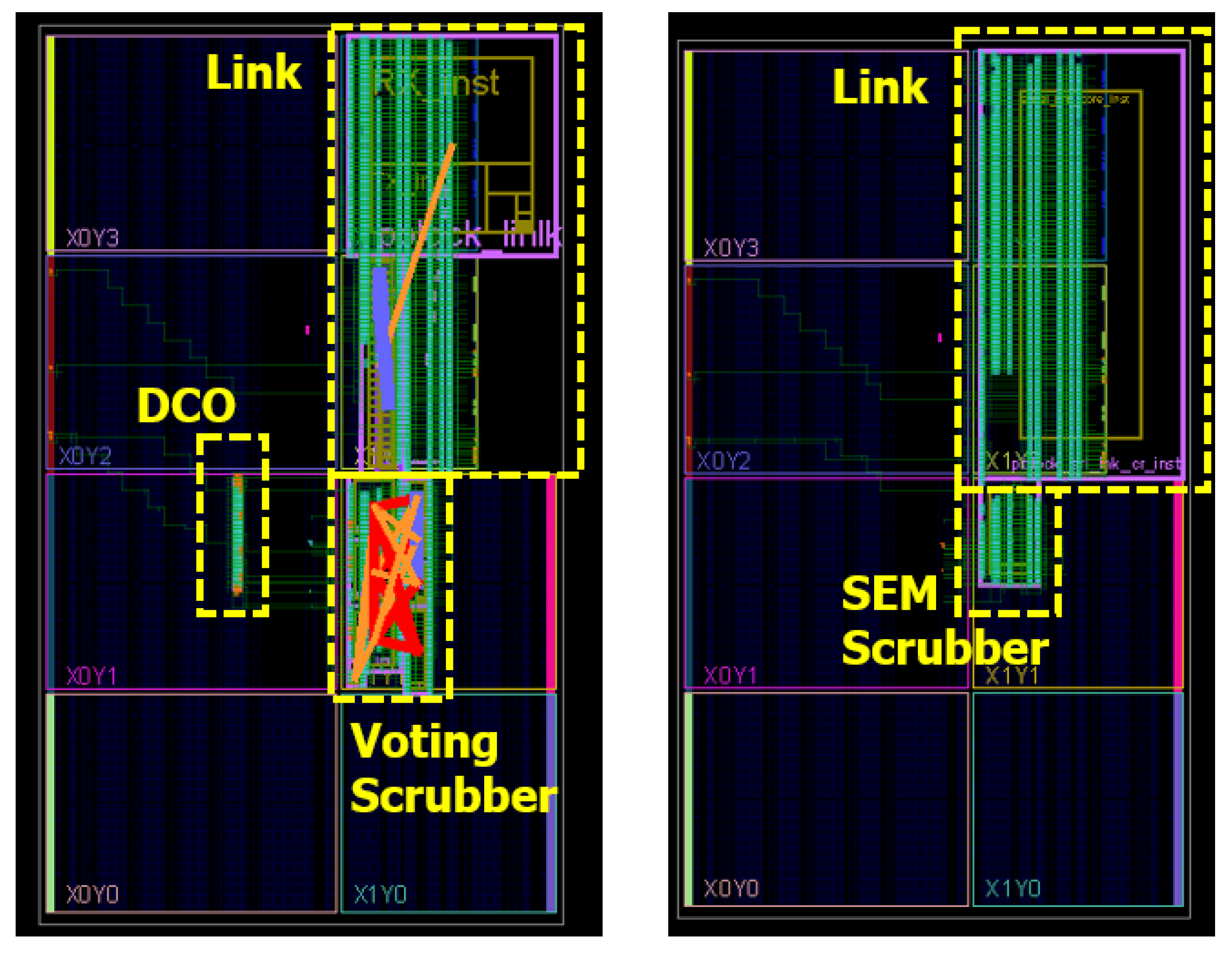
Figure 5. The layout of the externally-clocked voting scrubber (not shown) is very similar the DCO-clocked, the main difference being the lack of DCO-related resources. We floor-planned the design in order to constrain the link in just two clock regions, and the scrubber in a single clock region. Among the three scrubbers, the SEM has the lowest resource occupancy (
Table 1). The voting scrubber with external clock takes 503 slices and 9 BRAMs, while DCO-clocked requires 726 slices and 9 BRAMs. Although the resource utilization of voting scrubbers is higher than the SEM, it is important to underline that the above-mentioned figures are all tiny compared to the available resources of a modern medium-sized FPGA. For instance, in the device we used for our tests, the slice occupancy ranges between 7% (voting scrubber with external clock) and 2% (SEM), and the block RAM count between 6.7% and 3.3%.
We took care in minimizing the impact of the logic utilization on the configuration utilization. Since configuration frames run vertically in the device, we constrained placement and routing to be in regions as vertically-narrow as possible. In this way the number of configured frames for a given logic is minimized.
We performed the whole implementation by means of the Vivado design suite provided by Xilinx; no third-party triple modular redundancy (TMR) generation tools have been used.
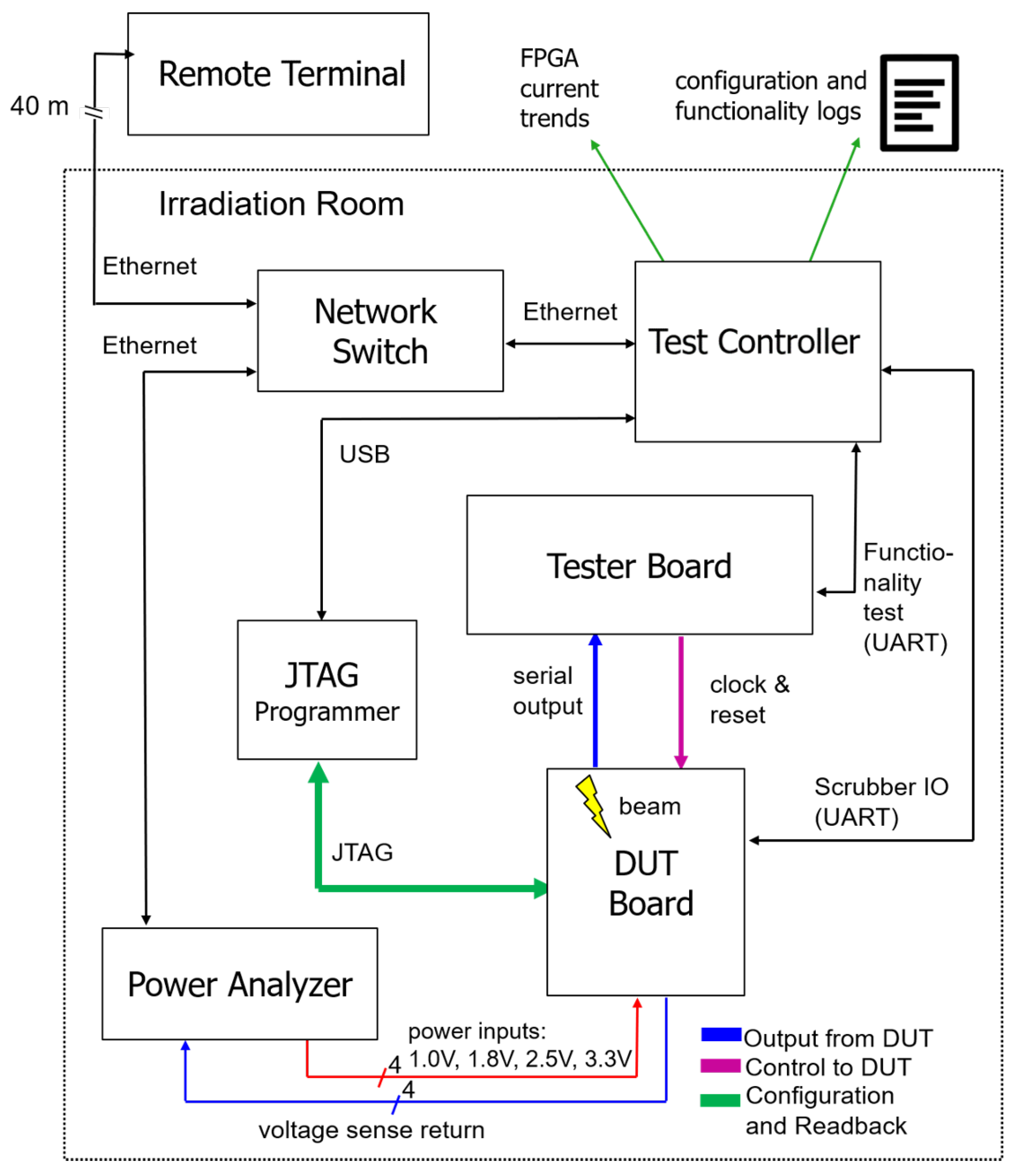
8. Test Setup
The test setup (
Figure 6) is built around the previously described DUT board. A dedicated power analyzer [
27] supplies the required power levels to the board and it monitors the current drawn by each channel. The main reason for this measurement is that SEUs in the configuration might impact the power consumption in FPGAs [
28]. The supply voltages are: VCCINT at 1.0 V for the core of the FPGA, VCCAUX at 1.8 V for the auxiliary power domain (DLLs, PLLs, and other special hardware), from which a 1.25 V reference is derived for gigabit transceivers, and VCCIO at 2.5 V and 3.3 V for the IO blocks. The tester board is an off-the-shelf KC705 [
29] and it implements a custom bit error ratio tester (BERT) we designed. The transmitter part of the BERT outputs a serial stream on a pair of coaxial cables to the DUT board. The link node in the DUT locks to the serial stream and echoes data back to the tester over another coaxial pair. The receiver part of the BERT de-serializes the data stream and checks the received parallel data against the transmitted ones. It logs any transmission error or loss of lock of the link via a UART to a dedicated personal computer (Test Controller, TC). The scrubber in the DUT is also interfaced to the via a UART to TC, which logs scrubbing status, including details about detected and correct upsets. Since the TC is in the irradiation room it needs to be operated remotely, another personal computer acts as a remote terminal to the TC.
9. Test Results
The tests described in this work were performed by means of a 62 MeV proton beam at Laboratori Nazionali del Sud (LNS), Catania, Italy in the “Zero Gradi” [
30] irradiation room. LNS provides an excellent dosimetry service, calibrated on a water target [
31,
32]. We derived the proton fluence from the dose measured by PTW monitor chambers. We used a beam spot with a 20 mm diameter, such to cover the whole FPGA die (11.0 mm in height by 6.2 mm in width). The beam profile (
Figure 7) was measured by means of a radiochromic film [
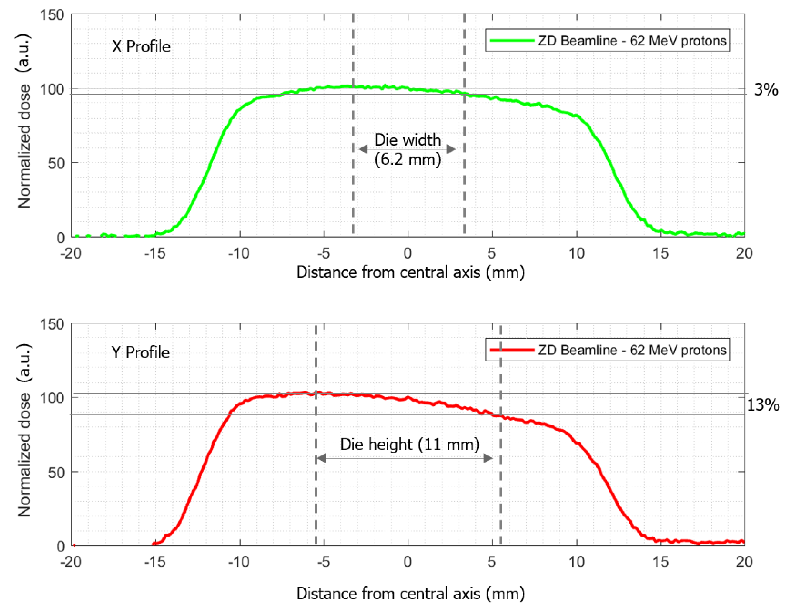
33] placed at the DUT position, at the end of the beam test. The full width half maximum of the transverse dose in x and y were measured to be, respectively, 23.7 mm and 23.6 mm. The homogeneity along the x and y axes were measured to be, respectively, below 3% and 13% (within DUT dimensions).
Our test was focused on measuring and comparing the impact of the three scrubbers on the reliability of our link design. For each test run, we followed this procedure:
power on the FPGA and configure it with the design of interest;
read configuration back and enable scrubbing;
start irradiation;
wait for unrecoverable failure of the link;
stop irradiation;
read configuration back and compare to the readback of Step 2; and
power off the FPGA.
Every ten seconds the tester board was resetting the link, which therefore was forced to re-lock. This periodic reset coupled to the scrubbing makes it possible to remove erroneous logic states induced by upsets and restart from scratch with the repaired configuration. We define a failure as unrecoverable if after two resets the link did not re-lock.
At Step 2, before enabling the scrubbing with the DCO and EXT firmwares, we configured the reset period for the PB to be a full scrubbing cycle, for both firmwares it is ∼1 s.
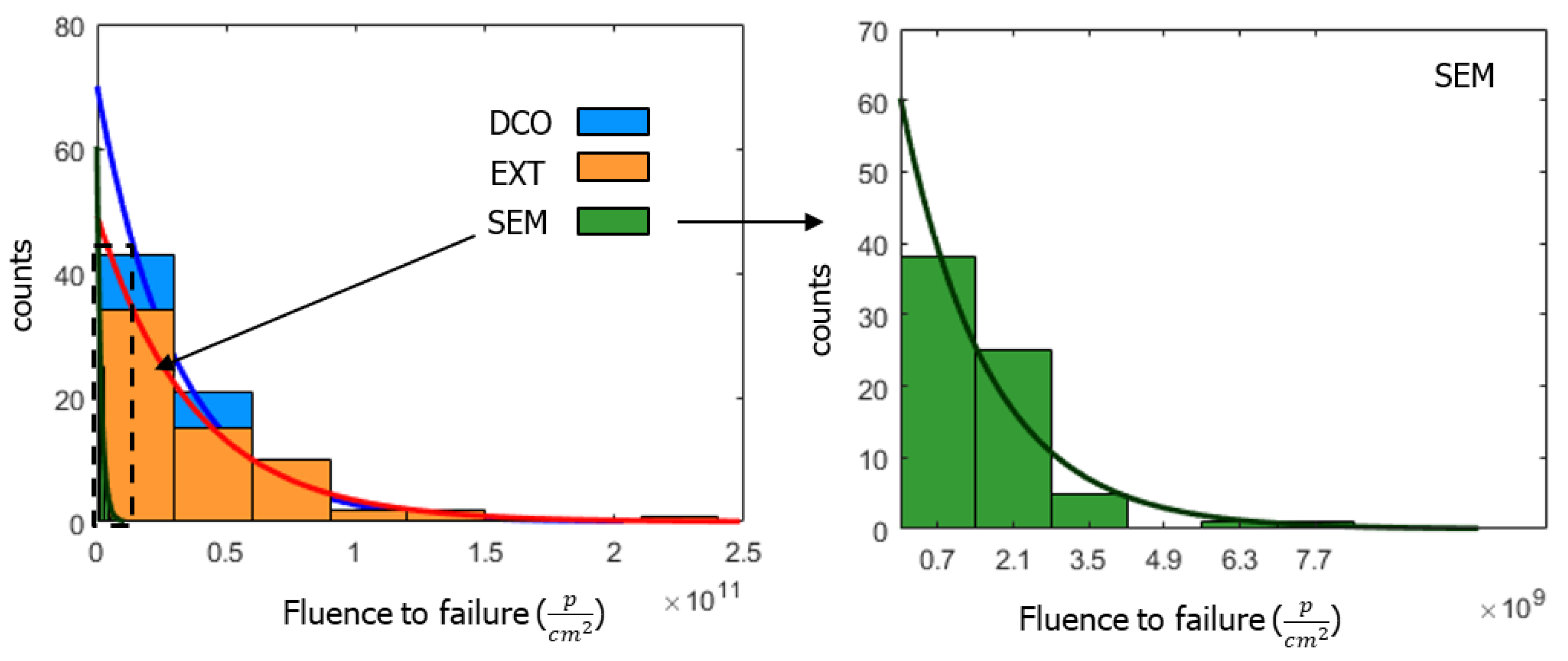
During Step 4, we also logged the possible failure of the scrubber. However, in most runs, the link failed unrecoverably before the scrubber due to its much higher cross section. We performed a total of 206 runs, i.e., around 70 runs for each design. Our results show that the EXT firmware reached the maximum fluence before failure among the three (3.7 × 10
10 p cm
−2); consequently, it showed the lowest cross section (2.7 × 10
−11 cm
2).
Table 2 provides more details for all the firmware architectures and
Figure 8 shows the distribution of the fluence to failure for all the test runs. The cross section of the DCO and SEM firmwares with respect to the EXT are, respectively, 1.2 and 23 times higher. The improvement of EXT versus DCO could be related to the slightly higher logic occupation and routing of the oscillator. One could suppose that the significant improvement the majority-voting scrubbers versus the SEM is likely related to their internal TMR, scrubbing of block RAM and scratchpad, and periodic processor reset. Unfortunately, Xilinx does not provide details about the SEM internal architecture, and the countermeasures taken against single event upsets, thus this hypothesis cannot be verified. However, we can state that the additional resource occupation of the majority-voting scrubbers is well compensated by the gain in reliability.
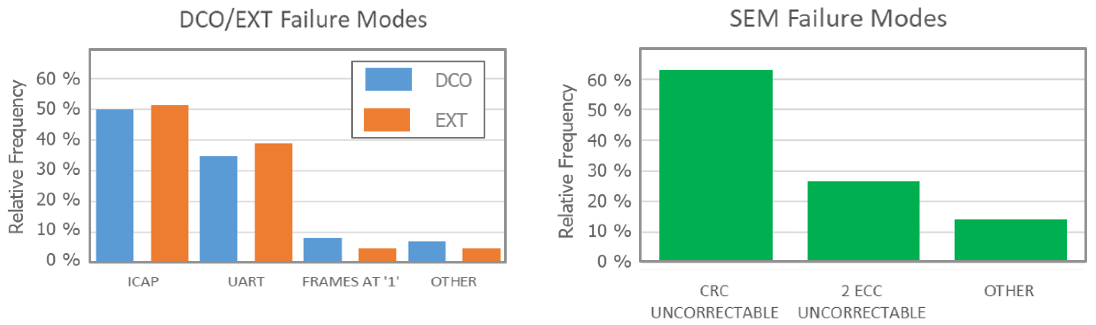
To gather information about the components of the logic causing the failure, we analyzed the failure modes of all the firmwares (
Figure 9). As far as it concerns the DCO and EXT firmwares, we grouped their failures in four main classes. The first class we defined (“ICAP”) is related to an incorrect communication through the ICAP. In fact, the scrubber assesses whether it can access the configuration by attempting to read the device IDCODE, a unique code used for JTAG identification of the part. Reading an incorrect IDCODE makes the scrubber retry to read it. Therefore, the scrubber enters a loop until a correct IDCODE is read. We consider a loop with more than 10 iterations as an ICAP failure. We defined a second class of failures (“UART”) in which the UART sends continuously incorrect ASCII characters to the TC and makes the terminal unreadable. The ICAP and UART failure classes include, respectively, 50% and 35% of the failures concerning the DCO firmware and 52% and 39% for the EXT firmware. We identified another distinct failure mode in which the scrubber starts to read back erroneously all the frames with all the bits set (“FRAMES1”), which for the DCO and EXT firmwares represents, respectively, 8% and 5% of the cases. Finally, we grouped all the remaining failures modes which we experienced as “OTHER”, 7% for DCO and 5% for EXT.
Nearly half of the failures are related to the access through the ICAP, and this aspect might be related to the fact that the ICAP could not be tripled. In addition, failures tagged as UART are also most likely related to the fact the output from the FPGA was not tripled. It is possible that in some runs the scrubber kept on operating correctly on configuration despite the failure of its UART output. However, even if this were the case, the link failed unrecoverably after a certain time, and this means the scrubber stopped working eventually. Since the UART output was no longer valid, it was not possible to determine the actual failure instant and the UART failure might have masked other failure modes. The “FRAMES1” failure is probably related to the ICAP remaining capable of reading the IDCODE, but failing to retrieve configuration frames.
As far as it concerns the SEM scrubber, we divided failures into three classes. The first class (“CRC uncorrectable”) includes failures in which the SEM was detecting a CRC error but it was unable to repair the error, 63% of the cases. The second class (“2 ECC uncorrectable”) includes failures in which the SEM detected a 2-bit upset in a frame, but was unable to correct the error. Finally, we used a third class (“OTHER”) to group all the other failures we measured. In all test runs, the SEM eventually stopped operation and it did not provide any output via UART to the TC.
10. Conclusions
Our novel scrubber does not require external golden configuration memories and has no a priori limitation on the number of errors which it can correct per configuration frame, while instead the Xilinx SEM is limited at 2 bits per frame. With respect to the SEM, our solution has a bigger resource occupation, 2.3 times for the version with externally-sourced clock and 3.2 times for the version with DCO. It is important to remark that the logic footprint of both versions is tiny compared to the available resources of a modern medium-sized FPGA. For instance, in the device we used for our tests, the slice occupancy ranges between 7.0% (DCO-clocked version) and 4.9% (externally-sourced-clock version). We tested the effectiveness of our scrubber and of the SEM on a serial link design which uses complex hard macros such as the GTX. Irradiation test results prove that the mean proton fluence tolerated before failure by our solution is 23 times higher with respect to the SEM.
Author Contributions
Conceptualization, R.G.; methodology, R.G.; software, R.G., D.B., and S.P.; validation, R.G., D.B., S.P., and R.C.; formal analysis, R.G., D.B., S.P., and R.C.; investigation, R.G., D.B., S.P., and R.C.; resources, R.G., D.B., S.P., and R.C.; data curation, R.G., and S.P.; writing-original draft preparation, R.G.; writing-review and editing, R.G.; visualization, R.G.; supervision, R.G.; project administration, R.G.; and funding acquisition, R.G.
Funding
This research was funded by Italian Ministry of Education, University and Research (MIUR), under the the Scientific Independence of Young Researchers (SIR) 2014 with grant No. RBSI14JOUV. The institutions which contributed to the results reported in this work have been listed on the first page as affiliations of the authors.
Acknowledgments
We wish to thank A. Boiano, A. Anastasio and A. Vanzanella from INFN Sezione di Napoli for their technical support, and G.A.P. Cirrone from INFN Laboratori Nazionali del Sud for their support during irradiation tests.
Conflicts of Interest
The authors declare no conflict of interest. The funders had no role in the design of the study; in the collection, analyses, or interpretation of data; in the writing of the manuscript, or in the decision to publish the results.
References
- French, M.; Jones, L.L.; Morrissey, Q.; Neviani, A.; Turchetta, R.; Fulcher, J.; Hall, G.; Noah, E.; Raymond, M.; Cervelli, G.; et al. Design and Results from the APV25, a Deep Sub-micron CMOS Front-End Chip for the CMS Tracker. Nucl. Instrum. Methods Phys. Res. Sec. A 2001, 466, 359–365. [Google Scholar] [CrossRef]
- Bosch, R.E.; de Parga, A.J.; Mota, B.; Musa, L. The ALTRO chip: A 16-channel A/D converter and digital processor for gas detectors. IEEE Trans. Nucl. Sci. 2003, 50, 2460–2469. [Google Scholar] [CrossRef]
- Bocci, V.; Petrolo, E.; Salamon, A.; Vari, R.; Veneziano, S. The coincidence matrix ASIC of the level-1 muon barrel trigger of the ATLAS experiment. IEEE Trans. Nucl. Sci. 2003, 50, 1078–1085. [Google Scholar] [CrossRef]
- Moreira, P.; Ballabriga, R.; Baron, S.; Bonacini, S.; Cobanoglu, O.; Faccio, F.; Fedorov, T.; Francisco, R.; Gui, P.; Hartin, P.; et al. The GBT Project. In Proceedings of the Topical Workshop on Electronics for Particle Physics, Paris, France, 21–25 September 2009; pp. 342–346. [Google Scholar] [CrossRef]
- Moreira, P. The LpGBT Project Status and Overview. Available online: https://indico.cern.ch/event/468486/contributions/1144369/attachments/1239839/1822836/aces.2016.03.08.pdf (accessed on 26 November 2017).
- Virtex UltraScale FPGAs Data Sheet: DC and AC Switching Characteristics DS893; Xilinx Inc.: San Jose, CA, USA, 2016.
- Series FPGAs Configuration User Guide; Xilinx Inc.: San Jose, CA, USA, 2016.
- Stratix 10 Device Overview S10-OVERVIEW; Altera Corp.: San Jose, CA, USA, 2015.
- Zhang, C.M.; Jazaeri, F.; Pezzotta, A.; Bruschini, C.E.; Borghello, G.; Faccio, F.; Mattiazzo, S.; Baschirotto, A.; Enz, C.C. Characterization of GigaRad Total Ionizing Dose and Annealing Effects on 28-nm Bulk MOSFETs. IEEE Trans. Nucl. Sci. 2017, 64, 2639–2647. [Google Scholar] [CrossRef]
- Alía, R.G.; Markus, B.; Francesco, C.; Salvatore, D.; Alfredo, F.; Simone, G.; Yacine, K.; Maria, K.; Anton, L.; Corinna, M.; et al. LHC and HL-LHC: Present and Future Radiation Environment in the High-Luminosity Collision Points and RHA Implications. IEEE Trans. Nucl. Sci. 2018, 65, 448–456. [Google Scholar] [CrossRef]
- Wirthlin, M. High-Reliability FPGA-Based Systems: Space, High-Energy Physics, and Beyond. Proc. IEEE 2015, 103, 379–389. [Google Scholar] [CrossRef]
- Quinn, H. Radiation effects in reconfigurable FPGAs. Semicond. Sci. Technol. 2017, 32, 044001. [Google Scholar] [CrossRef]
- Sterpone, L.; Violante, M. Analysis of the robustness of the TMR architecture in SRAM-based FPGAs. IEEE Trans. Nucl. Sci. 2005, 52, 1545–1549. [Google Scholar] [CrossRef]
- Herrera-Alzu, I.; Lopez-Vallejo, M. Design techniques for xilinx virtex FPGA configuration memory scrubbers. IEEE Trans. Nucl. Sci. 2013, 60, 376–385. [Google Scholar] [CrossRef]
- Berg, M.; Poivey, C.; Petrick, D.; Espinosa, D.; Lesea, A.; LaBel, K.A.; Friendlich, M.; Kim, H.; Phan, A. Effectiveness of Internal Versus External SEU Scrubbing Mitigation Strategies in a Xilinx FPGA: Design, Test, and Analysis. IEEE Trans. Nucl. Sci. 2008, 55, 2259–2266. [Google Scholar] [CrossRef]
- Stoddard, A.; Gruwell, A.; Zabriskie, P.; Wirthlin, M.J. A Hybrid Approach to FPGA Configuration Scrubbing. IEEE Trans. Nucl. Sci. 2017, 64, 497–503. [Google Scholar] [CrossRef]
- LogiCORE IP Soft Error Mitigation Controller v4.0; Xilinx Inc.: San Jose, CA, USA, 2013.
- Tonfat, J.; Kastensmidt, F.L.; Rech, P.; Reis, R.; Quinn, H.M. Analyzing the Effectiveness of a Frame-Level Redundancy Scrubbing Technique for SRAM-based FPGAs. IEEE Trans. Nucl. Sci. 2015, 62, 3080–3087. [Google Scholar] [CrossRef]
- Lavin, C.; Padilla, M.; Lamprecht, J.; Lundrigan, P.; Nelson, B.; Hutchings, B. RapidSmith: Do-it-yourself CAD tools for Xilinx FPGAs. In Proceedings of the 21st International Conference on Field Programmable Logic and Applications, Chania, Greece, 5–7 September 2011; pp. 349–355. [Google Scholar]
- Giordano, R.; Barbieri, D.; Perrella, S.; Catalano, R.; Milluzzo, G. Configuration Self-Repair in Xilinx FPGA. IEEE Trans. Nucl. Sci. 2018, 65, 2691–2698. [Google Scholar] [CrossRef]
- Giordano, R.; Perrella, S.; Izzo, V.; Milluzzo, G.; Aloisio, A. Redundant-Configuration Scrubbing of SRAM-Based FPGAs. IEEE Trans. Nucl. Sci. 2017, 64, 2497–2504. [Google Scholar] [CrossRef]
- Giordano, R. Method for Generating Redundant Configuration in FPGAs. U.S. Patent 16/348,810, 9 May 2019. [Google Scholar]
- Giordano, R. Method for Generating Redundant Configuration in FPGAs. PCT Application no. PCT/IB2018/060461, 20 December 2018. [Google Scholar]
- PicoBlaze 8-bit Embedded Microcontroller User Guide; Xilinx Inc.: San Jose, CA, USA, 2015.
- Kintex-7 FPGAs Data Sheet: DC and AC Switching Characteristics; Xilinx Inc.: San Jose, CA, USA, 2015.
- Giordano, R.; Ameli, F.; Bifulco, P.; Bocci, V.; Cadeddu, S.; Izzo, V.; Lai, A.; Mastroianni, S.; Aloisio, A. High-Resolution Synthesizable Digitally-Controlled Delay Lines. IEEE Trans. Nucl. Sci. 2015, 62, 3163–3171. [Google Scholar] [CrossRef]
- Agilent Technologies DC Power Analyzer Model N6705 User Guide; Agilent Technologies: Santa Clara, CA, USA, 2015.
- Aloisio, A.; Bocci, V.; Giordano, R.; Izzo, V.; Sterpone, L.; Violante, M. Power Consumption Versus Configuration SEUs in Xilinx Virtex-5 FPGAs. IEEE Trans. Nucl. Sci. 2013, 60, 3502–3507. [Google Scholar] [CrossRef]
- KC705 Evaluation Board for the Kintex-7 FPGA User Guide; Xilinx Inc.: San Jose, CA, USA, 2015.
- Bonanno, V.P.; Puglia, S.M.R.; Catalano, R.; Cirrone, G.A.P.; Cosentino, G.; Litrico, P.; Cuttone, G.; Mascali, D.; Musumeci, M.S.; Petringa, G.; et al. A radiation hardness test facility at INFN-LNS in the framework of ASIF project. Nucl. Instrum. Methods Phys. Res. Sec. B 2019, 461, 114–117. [Google Scholar] [CrossRef]
- Cirrone, G.A.P.; Cuttone, G.; Lojacono, P.A.; Nigro, S.L.; Mongelli, V.; Patti, I.V.; Privitera, G.; Raffaele, L. A 62-MeV Proton Beam for the Treatment of Ocular Melanoma at Laboratori Nazionali del Sud-INFN. IEEE Trans. Nucl. Sci. 2004, 51, 860–865. [Google Scholar] [CrossRef]
- Cuttone, G.; Cirrone, G.A.P.; Monaca, G.D.F.L.; Nigro, S.L.; Ott, J.; Pittera, S.; Privitera, G.; Raffaele, L.; Reibaldi, A.; Romano, F.; et al. CATANA protontherapy facility: The state of art of clinical and dosimetric experience. Eur. Phys. J. Plus 2011, 126, 65. [Google Scholar] [CrossRef]
- Zhao, L.; Das, I.J. Gafchromic EBT3 film dosimetry in proton beams. Phys. Med. Biol. 2010, 55, 291–301. [Google Scholar] [CrossRef] [PubMed]
© 2019 by the authors. Licensee MDPI, Basel, Switzerland. This article is an open access article distributed under the terms and conditions of the Creative Commons Attribution (CC BY) license (http://creativecommons.org/licenses/by/4.0/).


