High Dynamic Range Imaging with TDC-Based CMOS SPAD Arrays


Abstract
:1. Introduction
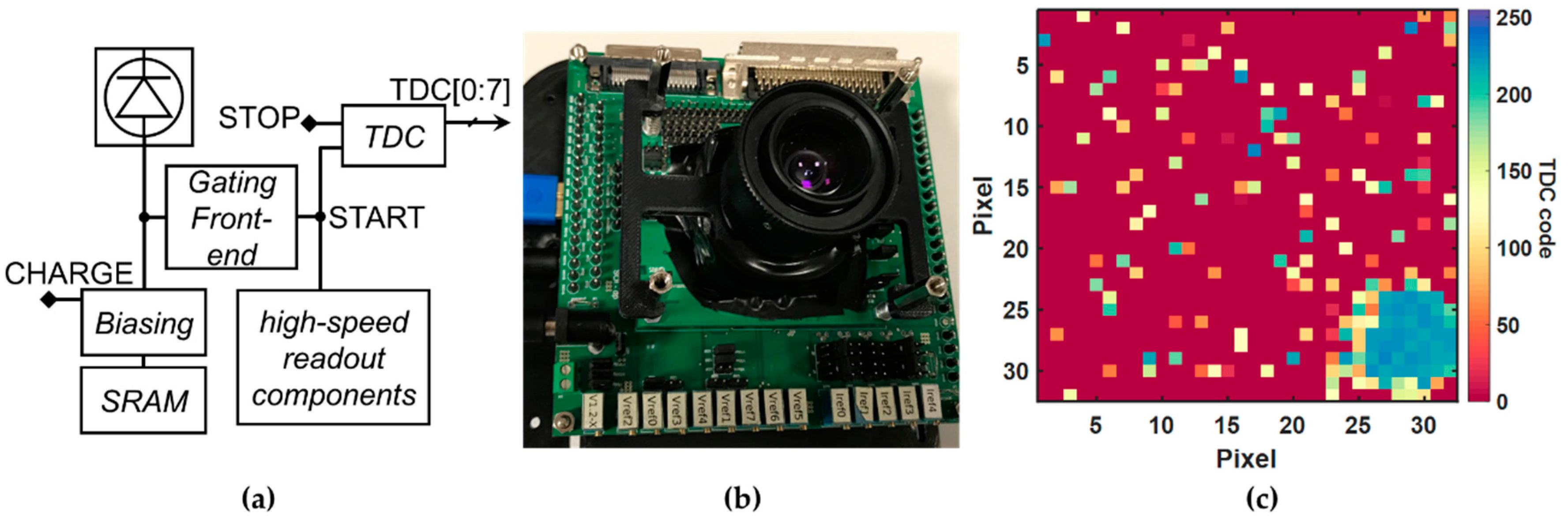
2. SuperEllen Chip
3. Dynamic Range of SPAD Arrays and Image Formation Model
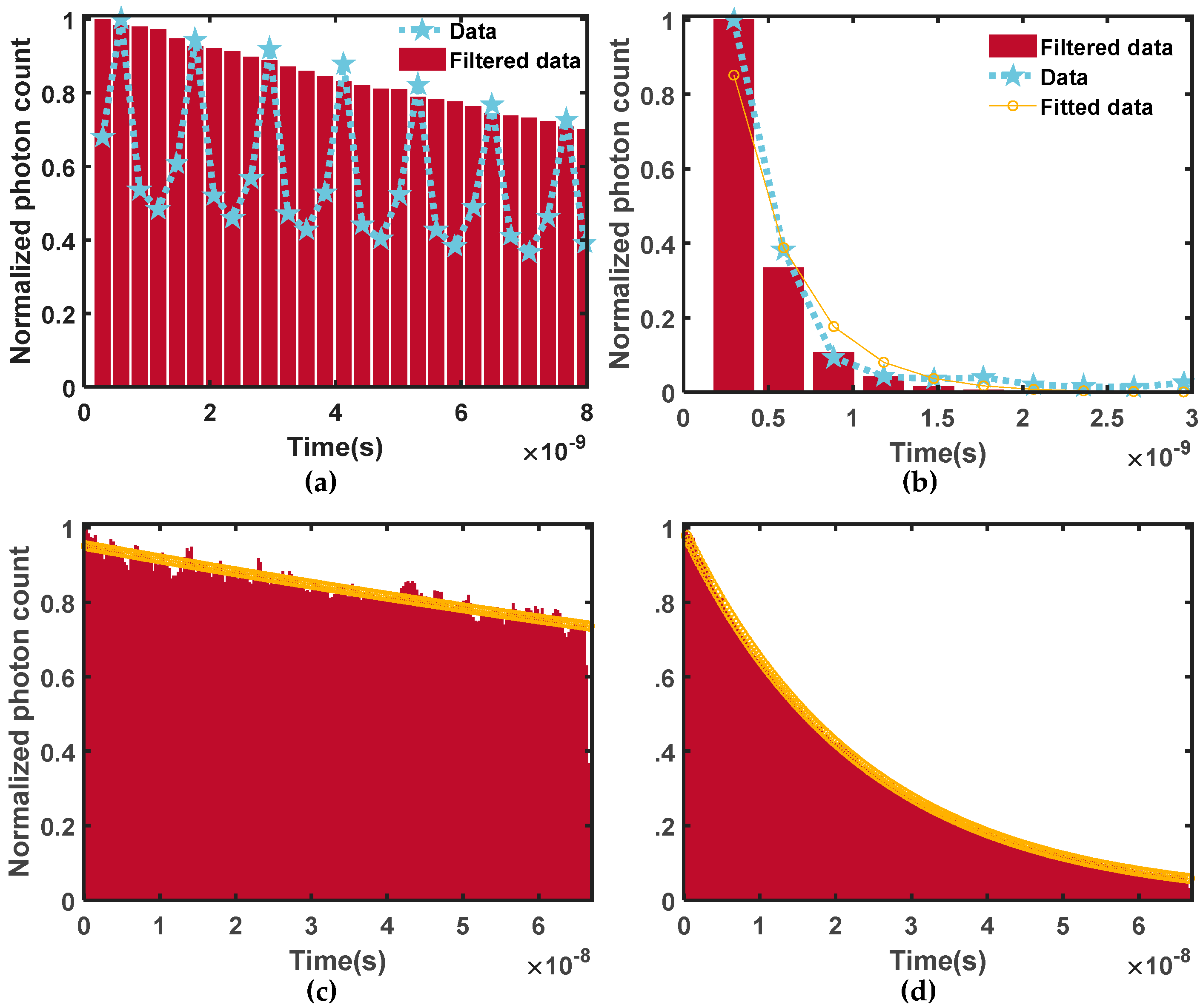
3.1. Low Flux
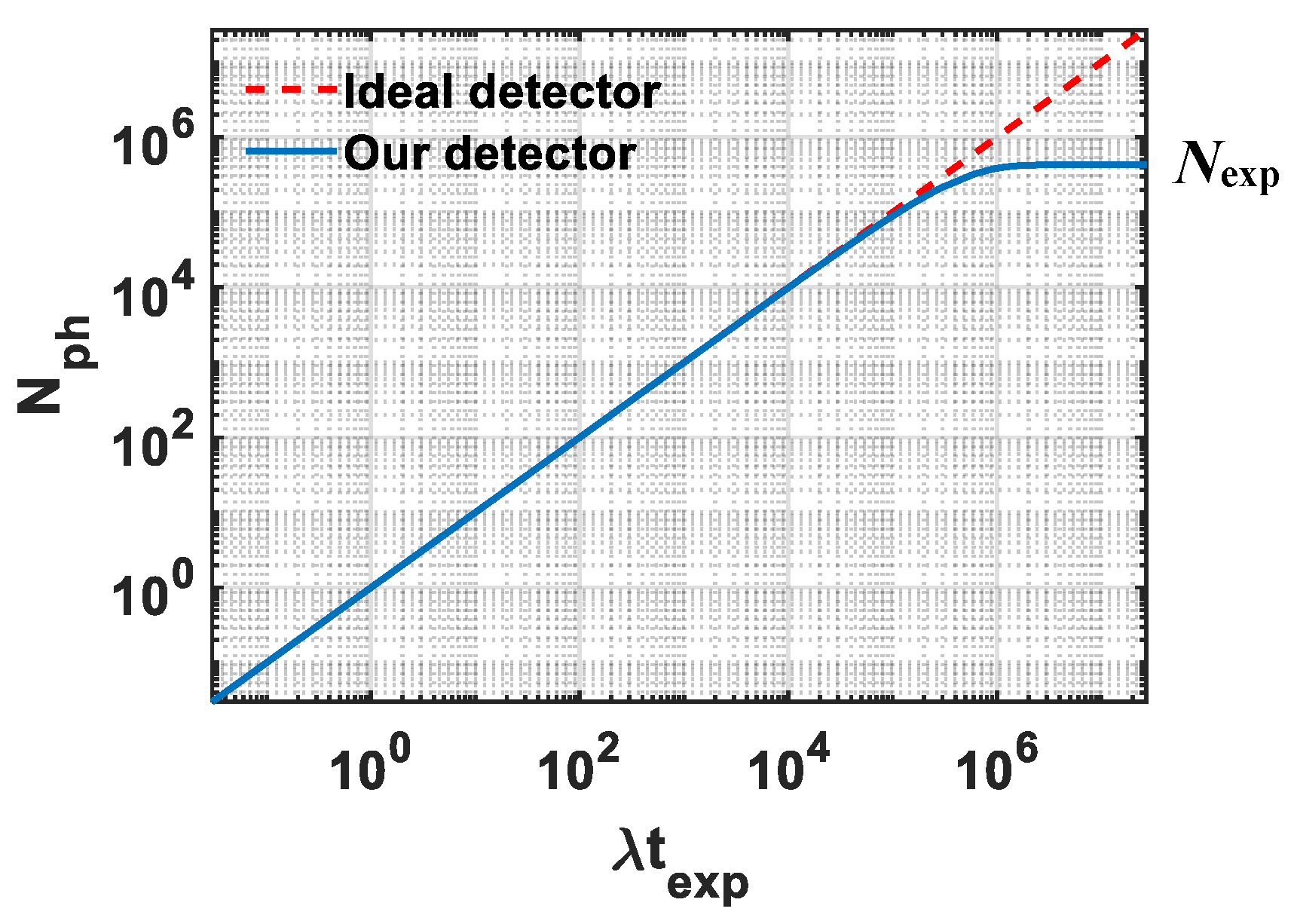
3.2. High Flux
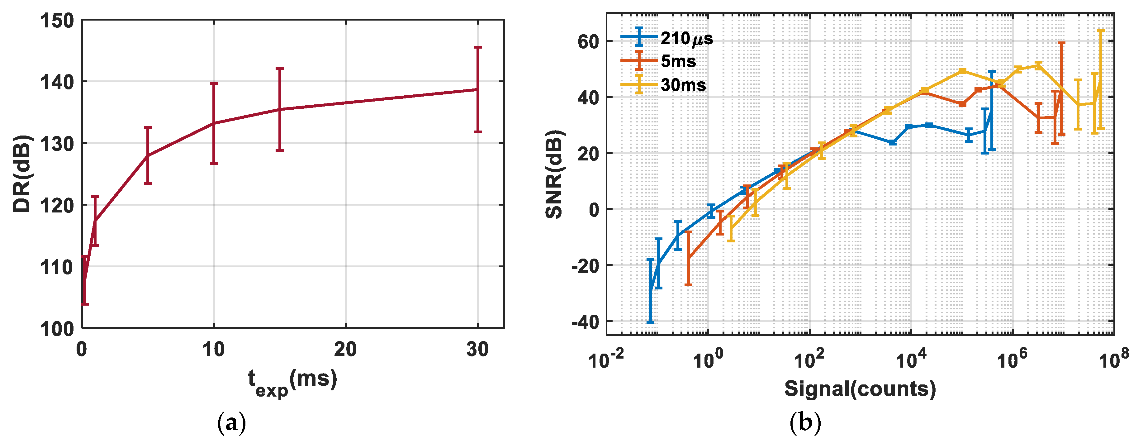
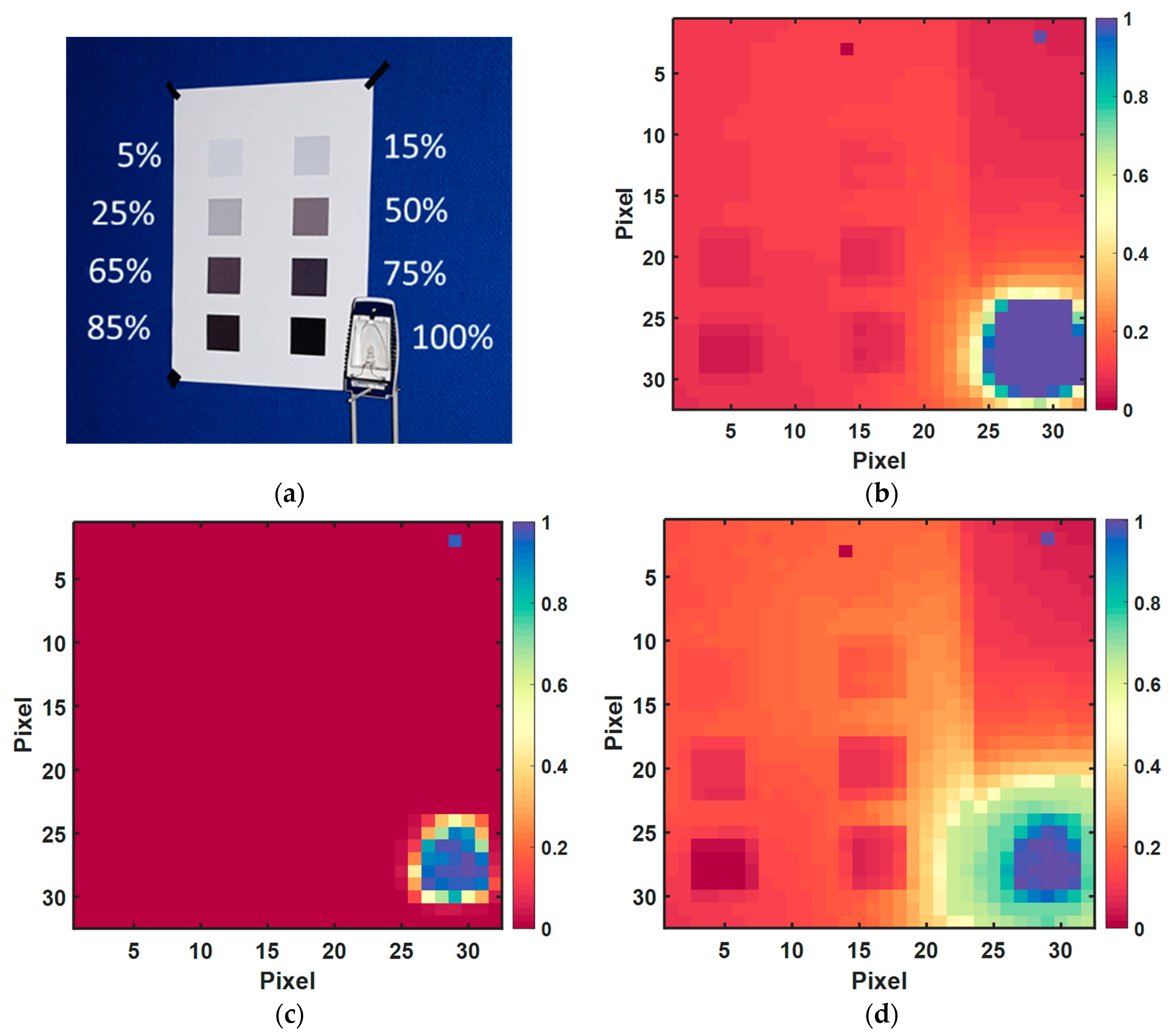
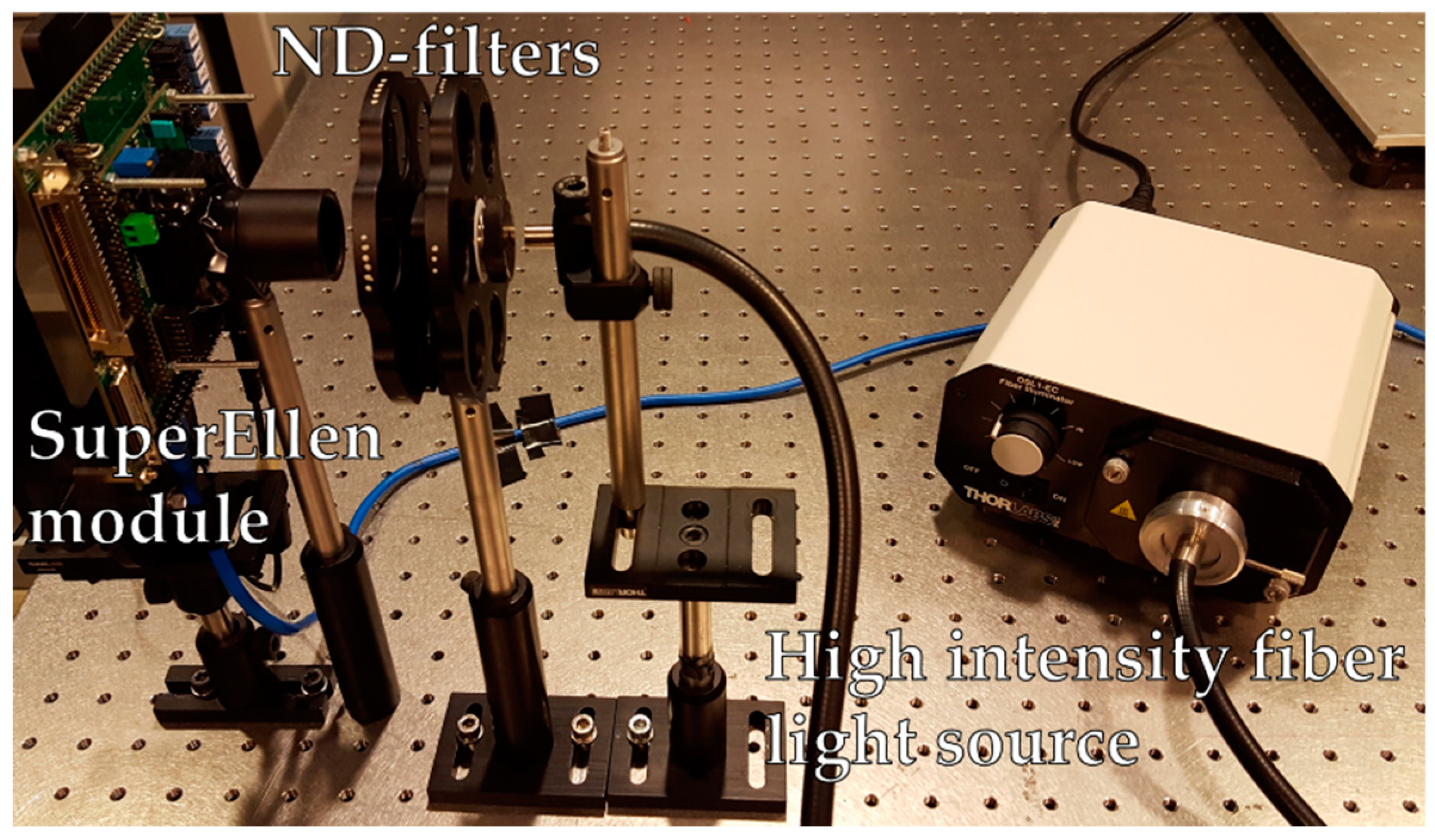
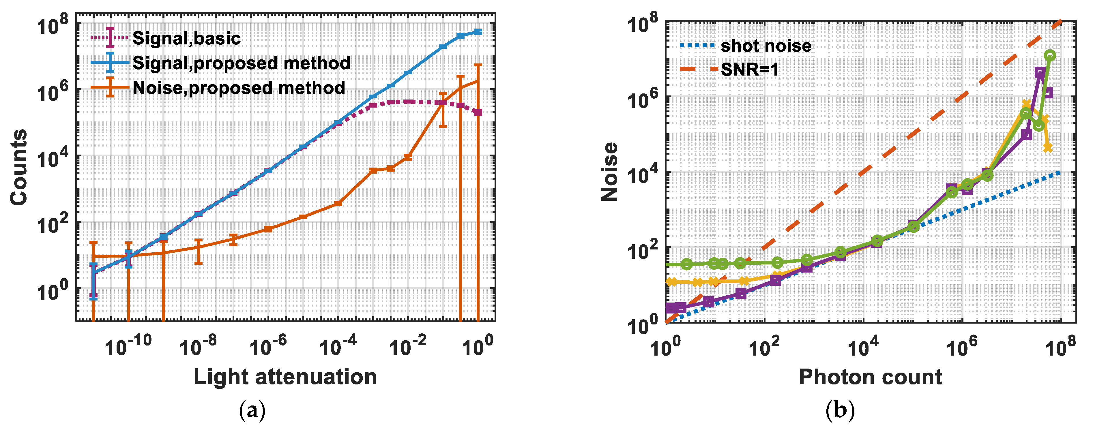
4. Experimental Results
5. Discussion
Author Contributions
Funding
Conflicts of Interest
References
- Heide, F.; Diamond, S.; Lindell, D.B.; Wetzstein, G. Sub-picosecond photon-efficient 3D imaging using single-photon sensors. Sci. Rep. 2018, 8, 17726. [Google Scholar] [CrossRef] [PubMed]
- Ingle, A.; Velten, A.; Gupta, M. High Flux Passive Imaging with Single-Photon Sensors. In Proceedings of the IEEE Conference on Computer Vision and Pattern Recognition (CVPR), Long Beach, CA, USA, 16–20 June 2019; pp. 6760–6769. [Google Scholar]
- Qian, X. Wide Dynamic Range CMOS Image Sensor for Star Tracking Applications; Nanyang Technological University: Singapore, 2015. [Google Scholar]
- Mori, M.; Sakata, Y.; Usuda, M.; Yamahira, S.; Kasuga, S.; Hirose, Y.; Kato, Y.; Tanaka, T. 6.6 A 1280 × 720 single-photon-detecting image sensor with 100dB dynamic range using a sensitivity-boosting technique. In Proceedings of the 2016 IEEE International Solid-State Circuits Conference (ISSCC), San Francisco, CA, USA, 31 January–4 February 2016; pp. 120–121. [Google Scholar]
- Guo, J.; Sonkusale, S. A High Dynamic Range CMOS Image Sensor for Scientific Imaging Applications. IEEE Sens. J. 2009, 9, 1209–1218. [Google Scholar] [CrossRef]
- Vargas-Sierra, S.; Liñán-Cembrano, G.; Rodríguez-Vázquez, Á. A 151 dB high dynamic range CMOS Image sensor chip architecture with tone mapping compression embedded In-Pixel. IEEE Sens. J. 2015, 15, 180–195. [Google Scholar] [CrossRef]
- Gamal, A.E.; Eltoukhy, H. CMOS image sensors. IEEE Circuits Devices Mag. 2005, 21, 6–20. [Google Scholar] [CrossRef]
- Kim, T. Wide dynamic range technologies: For mobile imaging sensor systems. IEEE Consum. Electron. Mag. 2014, 3, 30–35. [Google Scholar] [CrossRef]
- Spivak, A.; Belenky, A.; Fish, A.; Yadid-Pecht, O. Wide-Dynamic-Range CMOS Image Sensors—Comparative Performance Analysis. IEEE Trans. Electron. Devices 2009, 56, 2446–2461. [Google Scholar] [CrossRef]
- Dutton, N.A.; Abbas, T.A.; Gyongy, I.; Rocca, F.M.D.; Henderson, R.K. High Dynamic Range Imaging at the Quantum Limit with Single Photon Avalanche Diode-Based Image Sensors. Sensors 2018, 18, 16. [Google Scholar] [CrossRef] [PubMed]
- Fossum, E.R.; Ma, J.; Masoodian, S.; Anzagira, L.; Zizza, R. The quanta image sensor: every photon counts. Sensors 2016, 16, 25. [Google Scholar] [CrossRef] [PubMed]
- Fossum, E.R. Multi-Bit quanta image sensors. In Proceedings of the International Image Sensor Workshop (IISW), Vaals, The Netherlands, 8–11 June 2015; pp. 292–295. [Google Scholar]
- Bronzi, D.; Villa, F.; Tisa, S.; Tosi, A.; Zappa, F.; Durini, D.; Weyers, S.; Brockherde, W. 100 000 Frames/s 64 × 32 Single-Photon Detector Array for 2-D Imaging and 3-D Ranging. IEEE J. Sel. Top. Quantum Electron. 2014, 20, 354–363. [Google Scholar] [CrossRef]
- Veerappan, C.; Richardson, J.; Walker, R.; Li, D.; Fishburn, M.W.; Maruyama, Y.; Stoppa, D.; Borghetti, F.; Gersbach, M.; Henderson, R.K.; et al. A 160 × 128 single-photon image sensor with on-pixel 55ps 10b time-to-digital converter. In Proceedings of the 2011 IEEE International Solid-State Circuits Conference, San Francisco, CA, USA, 20–24 February 2011; pp. 312–314. [Google Scholar]
- Rocca, F.M.D.; Abbas, T.A.; Dutton, N.A.W.; Henderson, R.K. A high dynamic range SPAD pixel for time of flight imaging. In Proceedings of the 2017 IEEE sensors, Glasgow, UK, 29 Octtober–1 November 2017; pp. 1–3. [Google Scholar]
- Henderson, R.K.; Johnston, N.; Hutchings, S.W.; Gyongy, I.; Abbas, T.A.; Dutton, N.; Tyler, M.; Chan, S.; Leach, J. 5.7 A 256 × 256 40nm/90nm CMOS 3D-Stacked 120dB Dynamic-Range Reconfigurable Time-Resolved SPAD Imager. In Proceedings of the 2019 IEEE International Solid-State Circuits Conference—(ISSCC), San Francisco, CA, USA, 1–21 February 2019; pp. 106–108. [Google Scholar]
- Ceccarelli, F.; Acconcia, G.; Labanca, I.; Gulinatti, A.; Ghioni, M.; Rech, I. 152-dB Dynamic Range with a Large-Area Custom-Technology Single-Photon Avalanche Diode. IEEE Photonics Technol. Lett. 2018, 30, 391–394. [Google Scholar] [CrossRef]
- Antolovic, I.M.; Bruschini, C.; Charbon, E. Dynamic range extension for photon counting arrays. Opt. Express 2018, 26, 22234–22248. [Google Scholar] [CrossRef] [PubMed]
- Perenzoni, M.; Massari, N.; Perenzoni, D.; Gasparini, L.; Stoppa, D. A 160 × 120 Pixel Analog-Counting Single-Photon Imager with Time-Gating and Self-Referenced Column-Parallel A/D Conversion for Fluorescence Lifetime Imaging. IEEE J. Solid State Circuits 2016, 51, 155–167. [Google Scholar] [CrossRef]
- Stoppa, D.; Borghetti, F.; Richardson, J.; Walker, R.; Grant, L.; Henderson, R.K.; Gersbach, M.; Charbon, E. A 32×32-pixel array with in-pixel photon counting and arrival time measurement in the analog domain. In Proceedings of the 2009 ESSCIRC, Athens, Greece, 14–18 September 2009; pp. 204–207. [Google Scholar]
- Field, R.M.; Realov, S.; Shepard, K.L. A 100 fps, Time-Correlated Single-Photon-Counting-Based Fluorescence-Lifetime Imager in 130 nm CMOS. IEEE J. Solid State Circuits 2014, 49, 867–880. [Google Scholar] [CrossRef]
- Stoppa, D.; Simoni, A. Single-Photon Detectors for Time-of-Flight Range Imaging. In Single-Photon Imaging; Seitz, P., Theuwissen, A.J.P., Eds.; Springer Berlin Heidelberg: Berlin/Heidelberg, Germany, 2011; pp. 275–300. [Google Scholar] [CrossRef]
- Unternährer, M.; Bessire, B.; Gasparini, L.; Perenzoni, M.; Stefanov, A. Super-resolution quantum imaging at the Heisenberg limit. Optica 2018, 5, 5. [Google Scholar] [CrossRef]
- Gasparini, L.; Zarghami, M.; Xu, H.; Parmesan, L.; Garcia, M.M.; Unternährer, M.; Bessire, B.; Stefanov, A.; Stoppa, D.; Perenzoni, M. A 32 × 32-pixel time-resolved single-photon image sensor with 44.64 μm pitch and 19.48% fill-factor with on-chip row/frame skipping features reaching 800 kHz observation rate for quantum physics applications. In Proceedings of the 2018 IEEE International Solid-State Circuits Conference—(ISSCC), San Francisco, CA, USA, 11–15 February 2018; pp. 98–100. [Google Scholar]
- Xu, H.; Pancheri, L.; Betta, G.F.D.; Stoppa, D. Design and characterization of a p+/n-well SPAD array in 150nm CMOS process. Opt. Express 2017, 25, 14. [Google Scholar] [CrossRef]
- Zappa, F.; Tisa, S.; Tosi, A.; Cova, S. Principles and features of single-photon avalanche diode arrays. Sens. Actuators A Phys. 2007, 140, 103–112. [Google Scholar] [CrossRef]
- Mao, C.; Kong, X.; Ma, H.; Zhang, L.; Yan, F.; Bu, X. A 128 × 1 Pixels, High Dynamic Range SPAD Imager in 0.18 µm CMOS Technology. In Proceedings of the 2018 IEEE Sensors, New Delhi, India, 28–31 October 2018; pp. 1–4. [Google Scholar]


| Sensor | This Work | [27] | [6] | [13] | [16] | [4] | |
|---|---|---|---|---|---|---|---|
| Technology (nm) | 150 | 180 | 350 | 350 | 40/90 | 110 | |
| Detector | SPAD 32 × 32 | SPAD 128 × 1 | photodiode 180 × 148 | SPAD 64 × 32 | SPAD 256 × 256/64 × 64 | avalanche photodiode 1280 × 720 | |
| Architecture | TDC-based | Photon counting | Photon counting | Photon counting | Photon counting | ||
| Pixel pitch (µm) | 44.64 | 15 | 33 | 150 | 9.2/38.4 | 3.8 | |
| Fill factor | 19.48% | 4% | 0.8% | 3.14% | 51% | ||
| DCR | 240 @ Vex = 1.3 | 1-k @ Vex = 1.5 | 100 @ Vex = 5 | 20 @ Vex = 1.5 | 0.1 | ||
| SNR (dB) | 51.2 | 30 | 53.8 | ||||
| DR (dB) | 138.7 | 107 | 80 | 151.45 | 110 | 120 | 100 |
| Frame rate (fps) | 0.2 | 30 | 0.125 | 100 | 30 | 15 | |
| Integration time (ms) | 30 | 0.21 | 2 | 8000 | 10 | 33 | |
© 2019 by the authors. Licensee MDPI, Basel, Switzerland. This article is an open access article distributed under the terms and conditions of the Creative Commons Attribution (CC BY) license (http://creativecommons.org/licenses/by/4.0/).
Share and Cite
Zarghami, M.; Gasparini, L.; Perenzoni, M.; Pancheri, L. High Dynamic Range Imaging with TDC-Based CMOS SPAD Arrays. Instruments 2019, 3, 38. https://doi.org/10.3390/instruments3030038
Zarghami M, Gasparini L, Perenzoni M, Pancheri L. High Dynamic Range Imaging with TDC-Based CMOS SPAD Arrays. Instruments. 2019; 3(3):38. https://doi.org/10.3390/instruments3030038
Chicago/Turabian StyleZarghami, Majid, Leonardo Gasparini, Matteo Perenzoni, and Lucio Pancheri. 2019. "High Dynamic Range Imaging with TDC-Based CMOS SPAD Arrays" Instruments 3, no. 3: 38. https://doi.org/10.3390/instruments3030038
APA StyleZarghami, M., Gasparini, L., Perenzoni, M., & Pancheri, L. (2019). High Dynamic Range Imaging with TDC-Based CMOS SPAD Arrays. Instruments, 3(3), 38. https://doi.org/10.3390/instruments3030038