Tuning the Electrical Parameters of p-NiOx-Based Thin Film Transistors (TFTs) by Pulsed Laser Irradiation

 ,
,
Abstract
1. Introduction
2. Device Fabrication Details
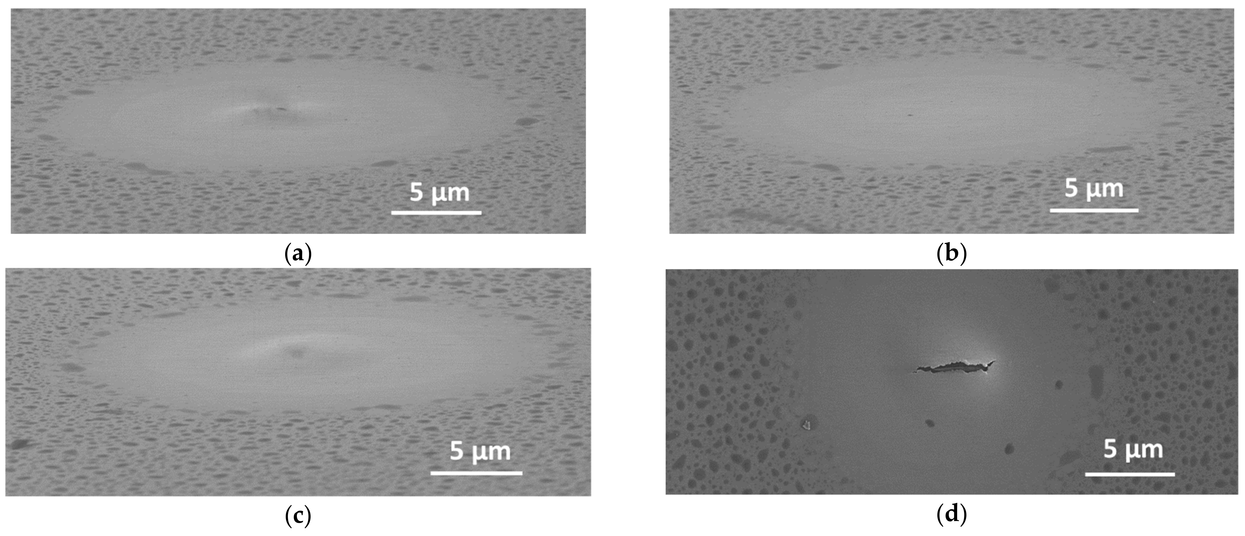
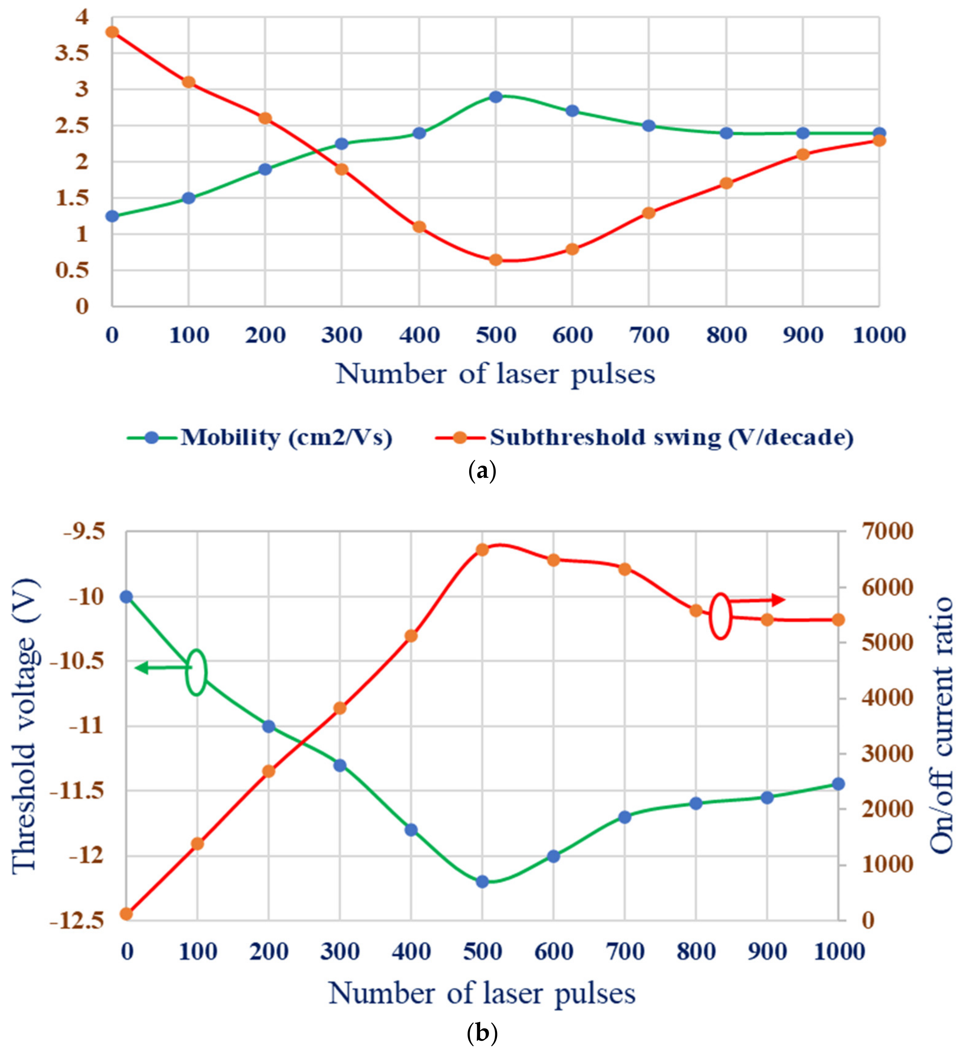
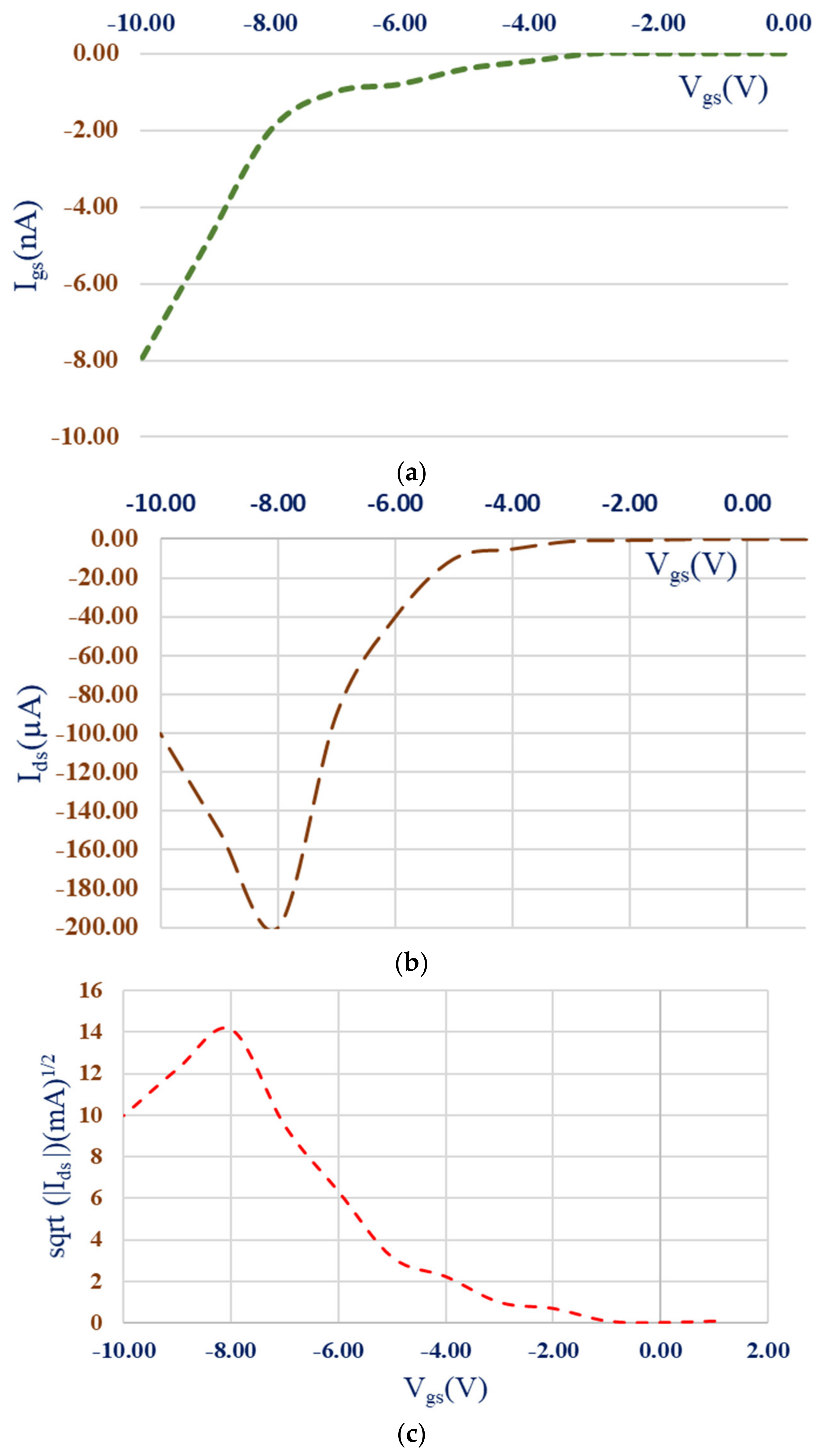
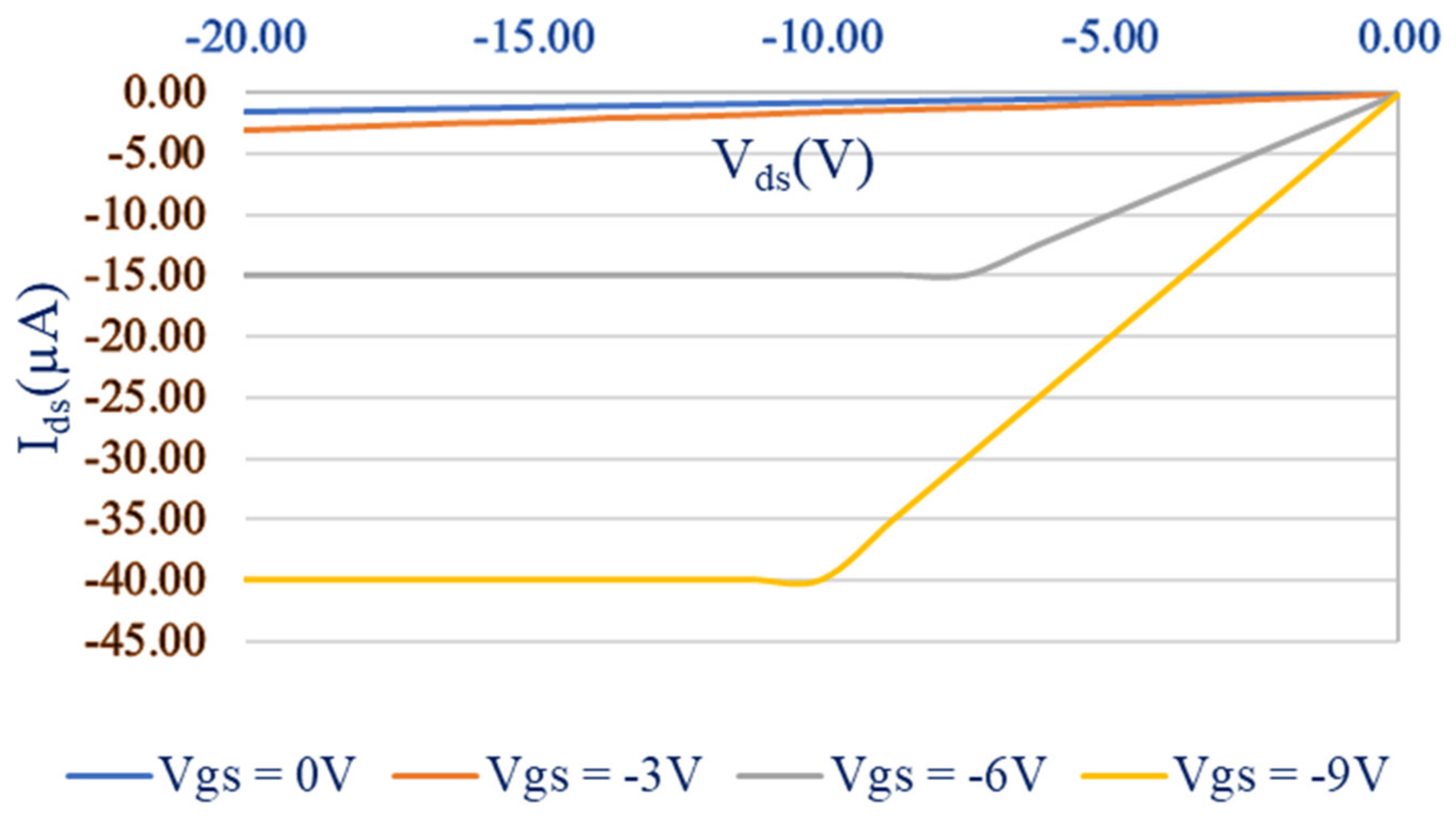
3. Results and Discussion
4. Conclusions
Author Contributions
Funding
Institutional Review Board Statement
Informed Consent Statement
Data Availability Statement
Acknowledgments
Conflicts of Interest
References
- Kim, H.J.; Park, K.; Kim, H.J. High-performance vacuum-processed metal oxide thin film transistors: A review of recent developments. J. Soc. Inf. Disp. 2020, 28, 591–622. [Google Scholar] [CrossRef]
- Pattanasattayavong, P.; Mottram, A.D.; Yan, F.; Anthopoulos, T.D. Study of the Hole Transport Processes in Solution-Processed Layers of the Wide Bandgap Semiconductor Copper(I) Thiocyanate (CuSCN). Adv. Funct. Mater. 2015, 25, 6802–6813. [Google Scholar] [CrossRef]
- Martins, R.F.P.; Ahnood, A.; Correia, N.; Pereira, L.M.N.P.; Barros, R.; Barquinha, P.M.C.B.; Costa, R.; Ferreira, I.M.M.; Nathan, A.; Fortunato, E.E.M.C. Recyclable, Flexible, Low-Power Oxide Electronics. Adv. Funct. Mater. 2013, 23, 2153–2161. [Google Scholar] [CrossRef]
- Kim, S.Y.; Ahn, C.H.; Lee, J.H.; Kwon, Y.H.; Hwang, S.; Lee, J.Y.; Cho, H.K. p-Channel Oxide Thin Film Transistors Using Solution-Processed Copper Oxide. ACS Appl. Mater. Interfaces 2013, 5, 2417–2421. [Google Scholar] [CrossRef]
- Khan, K.; Itapu, S.; Georgiev, D.G. Rectifying behavior and light emission from nickel oxide MIS structures. MRS Adv. 2016, 1, 3341–3347. [Google Scholar] [CrossRef]
- Khan, K.; Itapu, S.; Georgiev, D.G. Negative differential resistance (NDR) behavior of nickel oxide (NiO) based metal-insulator-semiconductor structures. J. Electron. Mater. 2020, 49, 333–340. [Google Scholar] [CrossRef]
- Borra, V.; Itapu, S.; Georgiev, D.G. Sn whisker growth mitigation by using NiO sublayers. J. Phys. D Appl. Phys. 2017, 50, 475309. [Google Scholar] [CrossRef]
- Manders, J.R.; Tsang, S.W.; Hartel, M.J.; Lai, T.H.; Chen, S.; Amb, C.M.; Reynolds, J.R.; So, F. Solution-Processed Nickel Oxide Hole Transport Layers in High-Efficiency Polymer Photovoltaic Cells. Adv. Funct. Mater. 2013, 23, 2993–3001. [Google Scholar] [CrossRef]
- Sato, H.; Minami, T.; Takata, S.; Yamada, T. Transparent conducting p-type NiO thin films prepared by magnetron sputtering. Thin Solid Films 1993, 236, 27–31. [Google Scholar] [CrossRef]
- Chen, S.C.; Kuo, T.Y.; Sun, T.H. Microstructures, electrical and optical properties of non-stoichiometric p-type nickel oxide films by radio frequency reactive sputtering. Surf. Coat. Technol. 2010, 205, S236–S240. [Google Scholar] [CrossRef]
- Chen, H.-L.; Lu, Y.-M.; Hwang, W.-S. Characterization of sputtered NiO thin films. Surf. Coat. Technol. 2005, 198, 138–142. [Google Scholar] [CrossRef]
- Reddy, Y.A.K. Influence of Growth Temperature on the Properties of DC Reactive Magnetron Sputtered NiO Thin Films. Int. J. Curr. Eng. Technol. 2013, 2, 351–357. [Google Scholar] [CrossRef]
- Subramanian, B.; Mohammed Ibrahim, M.; Murali, K.R.; Vidhya, V.S.; Sanjeeviraja, C.; Jayachandran, M. Structural, optoelectronic and electrochemical properties of nickel oxide films. J. Mater. Sci. Mater. Electron. 2009, 20, 953–957. [Google Scholar] [CrossRef]
- Agrawal, A.; Habibi, H.R.; Agrawal, R.K.; Cronin, J.P.; Roberts, D.M.; CaronPopowich, R.; Lampert, C.M. Effect of deposition pressure on the microstructure and electrochromic properties of electron-beam-evaporated nickel oxide films. Thin Solid Films 1992, 221, 239–253. [Google Scholar] [CrossRef]
- Yeh, W.; Matsumura, M. Chemical Vapor Deposition of Nickel Oxide Films from Bis-π-Cyclopentadienyl-Nickel. Jpn. J. Appl. Phys. 1997, 36 Pt 1, 6884–6887. [Google Scholar] [CrossRef]
- Guo, W.; Hui, K.N.; Hui, K.-S. High conductivity nickel oxide thin films by a facile sol-gel method. Mater. Lett. 2013, 92, 291–295. [Google Scholar] [CrossRef]
- Tanaka, M.; Mukai, M.; Fujimori, Y.; Kondoh, M.; Tasaka, Y.; Baba, H.; Usami, S. Transition metal oxide films prepared by pulsed laser deposition for atomic beam detection. Thin Solid Films 1996, 281–282, 453–456. [Google Scholar] [CrossRef]
- Reguig, B.A.; Khelil, A.; Cattin, L.; Morsli, M.; Bernède, J.C. Properties of NiO thin films deposited by intermittent spray pyrolysis process. Appl. Surf. Sci. 2007, 253, 4330–4334. [Google Scholar] [CrossRef]
- Kang, J.-K.; Rhee, S.-W. Chemical vapor deposition of nickel oxide films from Ni(C5H5)2O2. Thin Solid Films 2001, 391, 57–61. [Google Scholar] [CrossRef]
- Liu, H.; Zheng, W.; Yan, X.; Feng, B. Studies on electrochromic properties of nickel oxide thin films prepared by reactive sputtering. J. Alloys Compd. 2008, 462, 356–361. [Google Scholar] [CrossRef]
- Bruckner, W.; Kaltofen, R.; Thomas, J.; Hecker, M.; Uhlemann, M.; Oswald, S.; Elefant, D.; Schneider, C.M. Stress development in sputtered NiO thin films during heat treatment. J. Appl. Phys. 2003, 94, 4853. [Google Scholar] [CrossRef]
- Kuzmin, A.; Purans, J.; Rodionov, A. X-ray absorption spectroscopy study of the Ni K edge in magnetron-sputtered nickel oxide thin films. J. Phys. Condens. Matter 1997, 9, 6979–6993. [Google Scholar] [CrossRef]
- Itapu, S.; Borra, V.; Mossayebi, F. A computational study on the variation of bandgap due to native defects in stoichiometric NiO and Pd, Pt doping in stoichiometric NiO. Condens. Matter 2018, 3, 46. [Google Scholar] [CrossRef]
- Moening, J.P.; Georgiev, D.G. Formation of conical silicon tips with nanoscale sharpness by localized laser irradiation. J. Appl. Phys. 2010, 107, 14307. [Google Scholar] [CrossRef]
- Moening, J.P.; Thanawala, S.S.; Georgiev, D.G. Formation of high-aspect-ratio protrusions on gold films by localized pulsed laser irradiation. Appl. Phys. A 2009, 95, 635–638. [Google Scholar] [CrossRef]
- Lu, H.; Tu, Y.; Lin, X.; Fang, B.; Luo, D.; Laaksonen, A. Effects of laser irradiation on the structure and optical properties of ZnO thin films. Mater. Lett. 2010, 64, 2072–2075. [Google Scholar] [CrossRef]
- Kim, K.; Kim, S.; Lee, S.Y. Effect of excimer laser annealing on the properties of ZnO thin film prepared by sol-gel method. Curr. Appl. Phys. 2012, 12, 585–588. [Google Scholar] [CrossRef]
- Gupta, P.; Dutta, T.; Mal, S.; Narayan, J. Controlled p-type to n-type conductivity transformation in NiO thin films by ultraviolet-laser irradiation. J. Appl. Phys. 2012, 111, 13706. [Google Scholar] [CrossRef]
- Itapu, S.; Georgiev, D.G.; Uprety, P.; Podraza, N.J. Modification of reactively sputtered NiOx thin films by pulsed laser irradiation. Phys. Status Solidi (A) 2017, 214, 1600414. [Google Scholar]
- Abal’oshev, A.; Abal’osheva, I.; Gierłowski, P.; Lewandowski, S.J.; Konczykowski, M.; Rizza, G.; Chromik, Š. Effect of pulsed UV laser irradiation on the properties of crystalline YBa2Cu3O7−δ thin films. Supercond. Sci. Technol. 2007, 20, 433–440. [Google Scholar] [CrossRef]
- Chang, L.; Jiang, Y.; Ji, L. Improvement of the electrical and ferromagnetic properties in La0.67Ca0.33MnO3 thin film irradiated by CO2 laser. Appl. Phys. Lett. 2007, 90, 82505. [Google Scholar] [CrossRef]
- Ji, L.; Jiang, Y.; Wang, W.; Yu, Z. Enhancement of the dielectric permittivity of Ta2O5 ceramics by CO2 laser irradiation. Appl. Phys. Lett. 2004, 85, 1577–1579. [Google Scholar] [CrossRef]
- Papernov, S.; Kozlov, A.A.; Oliver, J.B.; Kessler, T.J.; Shvydky, A.; Marozas, B. Near-ultraviolet absorption annealing in hafnium oxide thin films subjected to continuous-wave laser radiation. Opt. Eng. 2014, 53, 122504. [Google Scholar] [CrossRef]
- Scorticati, D.; Illiberi, A.; Bor, T.; Eijt, S.W.H.; Schut, H.; Römer, G.R.B.E.; De Lange, D.F. Annealing of SnO2 thin films by ultra-short laser pulses. Opt. Express 2014, 22, A607. [Google Scholar] [CrossRef]
- Ichikawa, Y.; Chi, H.A.; Setsune, K.; Kawashima, S.I.; Kugimiya, K. Crystallization of Amorphous Titanium Oxide Thin Films by Pulsed UV-Laser Irradiation. MRS Proc. 1995, 397, 447. [Google Scholar] [CrossRef]
- Farooq, W.A.; Al Saud, M.; Alahmed, Z.A. Structural and optical properties of laser irradiated nanostructured cadmium oxide thin film synthesized by a sol-gel spin coating method. Opt. Spectrosc. 2016, 120, 745–750. [Google Scholar] [CrossRef]
- Hong, R.; Wei, C.; He, H.; Fan, Z.; Shao, J. Influences of CO2 laser irradiation on the structure and photoluminescence of zinc oxide thin films. Thin Solid Films 2015, 485, 262–266. [Google Scholar] [CrossRef]
- Liu, A.; Liu, G.; Zhu, H.; Shin, B.; Fortunato, E.; Matins, R.; Shan, F. Hole mobility modulation of solution-processed nickel oxide thin-film transistor based on high-k dielectric. Appl. Phys. Lett. 2016, 108, 233506. [Google Scholar] [CrossRef]
- Shan, F.; Liu, A.; Zhu, H.; Kong, W.; Liu, J.; Shin, B.; Fortunato, E.; Martins, R.; Liu, G. High-mobility p-type NiOx thin-film transistors processed at low temperatures with Al2O3 high-k dielectric. J. Mater. Chem. C 2016, 4, 9438–9444. [Google Scholar] [CrossRef]
- Xu, W.; Zhang, J.; Li, Y.; Zhang, L.; Chen, L.; Zhu, D.; Cao, P.; Liu, W.; Han, S.; Liu, X.; et al. p-type transparent amorphous oxide thin-film transistors using low-temperature solution-processed nickel oxide. J. Alloys Compd. 2019, 806, 40–51. [Google Scholar] [CrossRef]
- Shang, Z.W.; Hsu, H.H.; Zheng, Z.W.; Cheng, C.H. Progress and challenges in p-type oxide based thin film transistors. Nanotechnol. Rev. 2019, 8, 422–443. [Google Scholar] [CrossRef]
- Jiang, J.; Wang, X.H.; Zhang, Q.; Li, J.Q.; Zhang, X.X. Thermal oxidation of Ni films for p-type thin-film transistors. Phys. Chem. Chem. Phys. 2013, 15, 6875. [Google Scholar] [CrossRef]
- Chen, Y.; Sun, Y.; Dai, X.; Zhang, B.; Ye, Z.; Wang, M.; Wu, H. Tunable electrical properties of NiO thin films and p-type thin-film transistors. Thin Solid Films 2015, 592, 195–199. [Google Scholar] [CrossRef]
- Lin, T.; Li, X.; Jang, J. High-performance p-type NiOx thin-film transistor by Sn doping. Appl. Phys. Lett. 2016, 108, 233503. [Google Scholar] [CrossRef]
- Lin, A.; Zhu, H.; Guo, Z.; Meng, Y.; Liu, G.; Fortunato, E.; Martins, R.; Shan, F. Solution combustion synthesis: Low-temperature processing of p-type Cu:NiO thin films for transparent electronics. Adv. Mater. 2017, 29, 1701599. [Google Scholar]


| Ref. | Published Year | Oxide Layer | Mobility (cm2/V-s) | Subthreshold Swing (V/decade) | On/off Current Ratio | Threshold Voltage (V) |
|---|---|---|---|---|---|---|
| [42] | 2013 | NiO | 5.20 | 3.91 | 2.2 × 10³ | - |
| [43] | 2015 | NiO | 0.05 | 2.6 | 103 | 8.6 |
| [44] | 2016 | Sn:NiOx | 0.97 | 0.24 | 106 | 1.44 |
| [45] | 2017 | Cu:NiOx | 1.53 | 0.13 | 3 × 10⁴ | 0.45 |
| This work | 2021 | NiOx | 3.00 | 0.65 | 6.5 × 10⁴ | −12.5 |
Publisher’s Note: MDPI stays neutral with regard to jurisdictional claims in published maps and institutional affiliations. |
© 2021 by the authors. Licensee MDPI, Basel, Switzerland. This article is an open access article distributed under the terms and conditions of the Creative Commons Attribution (CC BY) license (https://creativecommons.org/licenses/by/4.0/).
Share and Cite
Manojreddy, P.; Itapu, S.; Ravali, J.K.; Sakkarai, S. Tuning the Electrical Parameters of p-NiOx-Based Thin Film Transistors (TFTs) by Pulsed Laser Irradiation. Condens. Matter 2021, 6, 21. https://doi.org/10.3390/condmat6020021
Manojreddy P, Itapu S, Ravali JK, Sakkarai S. Tuning the Electrical Parameters of p-NiOx-Based Thin Film Transistors (TFTs) by Pulsed Laser Irradiation. Condensed Matter. 2021; 6(2):21. https://doi.org/10.3390/condmat6020021
Chicago/Turabian StyleManojreddy, Poreddy, Srikanth Itapu, Jammalamadaka Krishna Ravali, and Selvendran Sakkarai. 2021. "Tuning the Electrical Parameters of p-NiOx-Based Thin Film Transistors (TFTs) by Pulsed Laser Irradiation" Condensed Matter 6, no. 2: 21. https://doi.org/10.3390/condmat6020021
APA StyleManojreddy, P., Itapu, S., Ravali, J. K., & Sakkarai, S. (2021). Tuning the Electrical Parameters of p-NiOx-Based Thin Film Transistors (TFTs) by Pulsed Laser Irradiation. Condensed Matter, 6(2), 21. https://doi.org/10.3390/condmat6020021