Article

The Effect of Point Defects on the Electronic Density of States of ScMN2-Type (M = V, Nb, Ta) Phases

1
Thin Film Physics Division, Department of Physics, Chemistry and Biology (IFM), Linköping university, SE-581 83 Linköping, Sweden
2
Theoretical Physics Division, Department of Physics, Chemistry and Biology (IFM), Linköping university, SE-581 83 Linköping, Sweden
*
Authors to whom correspondence should be addressed.
Condens. Matter 2019, 4(3), 70; https://doi.org/10.3390/condmat4030070
Submission received: 15 April 2019 / Revised: 10 July 2019 / Accepted: 11 July 2019 / Published: 15 July 2019

Abstract

:
ScMN2-type (M = V, Nb, Ta) phases are layered materials that have been experimentally reported for M = Ta and Nb. They are narrow-bandgap semiconductors with potentially interesting thermoelectric properties. Point defects such as dopants and vacancies largely affect these properties, motivating the need to investigate these effects. In particular, asymmetric peak features in the density of states (DOS) close to the highest occupied state is expected to increase the Seebeck coefficient. Here, we used first principles calculations to study the effects of one vacancy or one C, O, or F dopant on the DOS of the ScMN2 phases. We used density functional theory to calculate formation energy and the density of states when a point defect is introduced in the structures. In the DOS, asymmetric peak features close to the highest occupied state were found as a result of having a vacancy in all three phases. Furthermore, one C dopant in ScTaN2, ScNbN2, and ScVN2 implies a shift of the highest occupied state into the valence band, while one O or F dopant causes a shift of the highest occupied state into the conduction band.

1. Introduction

Vacancies, dopants, and other point defects are important for controlling or tuning the properties of materials [1,2,3]. This is particularly valid for semiconductors and thermoelectric materials. The understanding of semiconductive and thermoelectric materials is increased by studying the density of states (DOS) [4,5,6]. The electronic structure close to the Fermi level in the DOS of a thermoelectric material can be affected by the introduction of defects or impurities, which in turn alter the conductivity (σ), and thus may improve the thermoelectric power factor (S2σ) and maximize the figure of merit (ZT). Here Z = S2σ/κ, where S is the Seebeck coefficient, κ the total thermal conductivity, and T the absolute temperature [7,8]. These quantities are affected by peak features introduced close to the Fermi level, or when the Fermi level is shifted as a result of the introduction of point defects [4,9,10].
ScN-based and CrN-based materials for thermoelectrics have shown remarkably high thermoelectric power factors [7,11]. However, in their pure form, the thermal conductivity of ScN is too high for thermoelectric applications, which leads to a moderate figure of merit [7,11]. Different strategies to decrease the thermal conductivity are alloying [12,13,14,15], artificial superlattices [16,17,18,19], and nanostructuring as exemplified with CrN [20]. The alloying of ScN with Mg can increase the figure of merit and turn the material p-type, if the dopant level is sufficient [21]. Recently, we proposed, based on ab initio calculations, that also ScTaN2, ScNbN2, and ScVN2 could be of interest in this context. We found that these materials have anisotropic thermoelectric properties that can be tuned by doping [22]. Synthesis of ScTaN2 and ScNbN2 has also shown that the phases could be deficient of nitrogen [23,24]. Furthermore, it is known that ScN can incorporate impurities and dopants, which in turn affect the thermoelectric properties [25,26,27].
The layered phases ScTaN2 and ScNbN2, which have been observed experimentally [23,24,28], have a similar laminar structure to the more well-known “211” MAX phases, which have the stoichiometric formula M2AX and where M is a transition metal, A an A-group element and X carbon or nitrogen [29,30,31]. The structure of ScTaN2 is comprised of ScN6/3 octahedra and TaN6/3 prisms. Sc occupies the 2a positions, Ta the 2d positions, and N the 4f positions [28], which are the inversed Wyckoff positions of a “211” MAX phase. This structure can therefore be described as an “inverse MAX phase” [22]. ScVN2 has not been observed to exist experimentally, but is expected to be able to be synthesized based on thermodynamic and elastic stability calculations [12,22]. Here, we investigate the effect of one vacancy or one dopant on the electronic DOS close to the highest occupied state of ScTaN2, ScNbN2, and ScVN2.

2. Computational Details

The calculations were performed using the Vienna ab initio simulation package (VASP) [32,33,34,35], which implements density functional theory (DFT) based on the Kohn–Sham equations [36] and the projector augmented wave method (PAW) [37]. The exchange–correlation potential was modeled with generalized gradient approximation according to Perdew, Burke, and Ernzerhof (GGA-PBE) [38]. The cutoff energy for the plane waves was set to 650 eV. We used supercells that were 3 × 3 × 2 conventional hexagonal unit cells consisting of 144 atoms for ScTaN2, ScNbN2, and ScVN2. For the conventional unit cells, we used previously calculated lattice parameters [22].
The considered defects are individual point defects in ScTaN2, ScNbN2, and ScVN2 introduced by replacing N with one vacancy, or one C, O, or F atom. Accordingly, the defect concentration was in all cases 1.4 at. % (i.e., one atom out of 72). The energy of formation of one vacancy, Ef(vac), was calculated as follows:
E f ( v a c ) = E t o t ( v a c ) M 1 M E t o t ( b u l k ) .
Etot(vac) is the total energy of a supercell, where one nitrogen atom is replaced by a vacancy, Etot(bulk) is the total energy of the supercell without any defect, and M the total number of atoms in that supercell. For a dopant, X, the energy of formation, Ef(X), was calculated as follows:
E f ( X ) = E t o t ( X ) E t o t ( b u l k ) + µ x µ N .
Etot(X) is the total energy of a supercell containing the dopant, µx is the chemical potential of the dopant, and µN is the chemical potential of nitrogen. For the chemical potentials of N, F, and O, these are the half of the energy of the corresponding dimers. For the dimer calculations, two atoms were placed in a box that was 16–18 times greater than the atomic distance. A 1 × 1 × 1 k-point mesh was used. Total energy was optimized with respect to the interatomic distance. For C, the energy of one carbon atom was calculated in the diamond structure using an 8-atom cell, and an 8 × 8 × 8 k-point mesh was used.
We also considered the formation enthalpy relative to the binary phases in order to determine the phase stability of the phases when Sc is replaced by Y. This is defined for YMN2, where M is Ta, Nb, or V, as
Δ H = H Y M N 2 H Y N H M N .
Each enthalpy, H, is considered at zero pressure and the energy of each phase is taken at its equilibrium volume. The energy and force tolerances for the structural relaxation were 0.0001 eV and 0.001 eV/Å, respectively.
In order to calculate the electronic DOS, a k-point mesh of 5 × 5 × 3 was used. For integration over the Brillouin zone, the tetrahedron method with Blöchl correction [39] was used in all DOS calculations. The value of the level broadening was set to 0.2 eV.

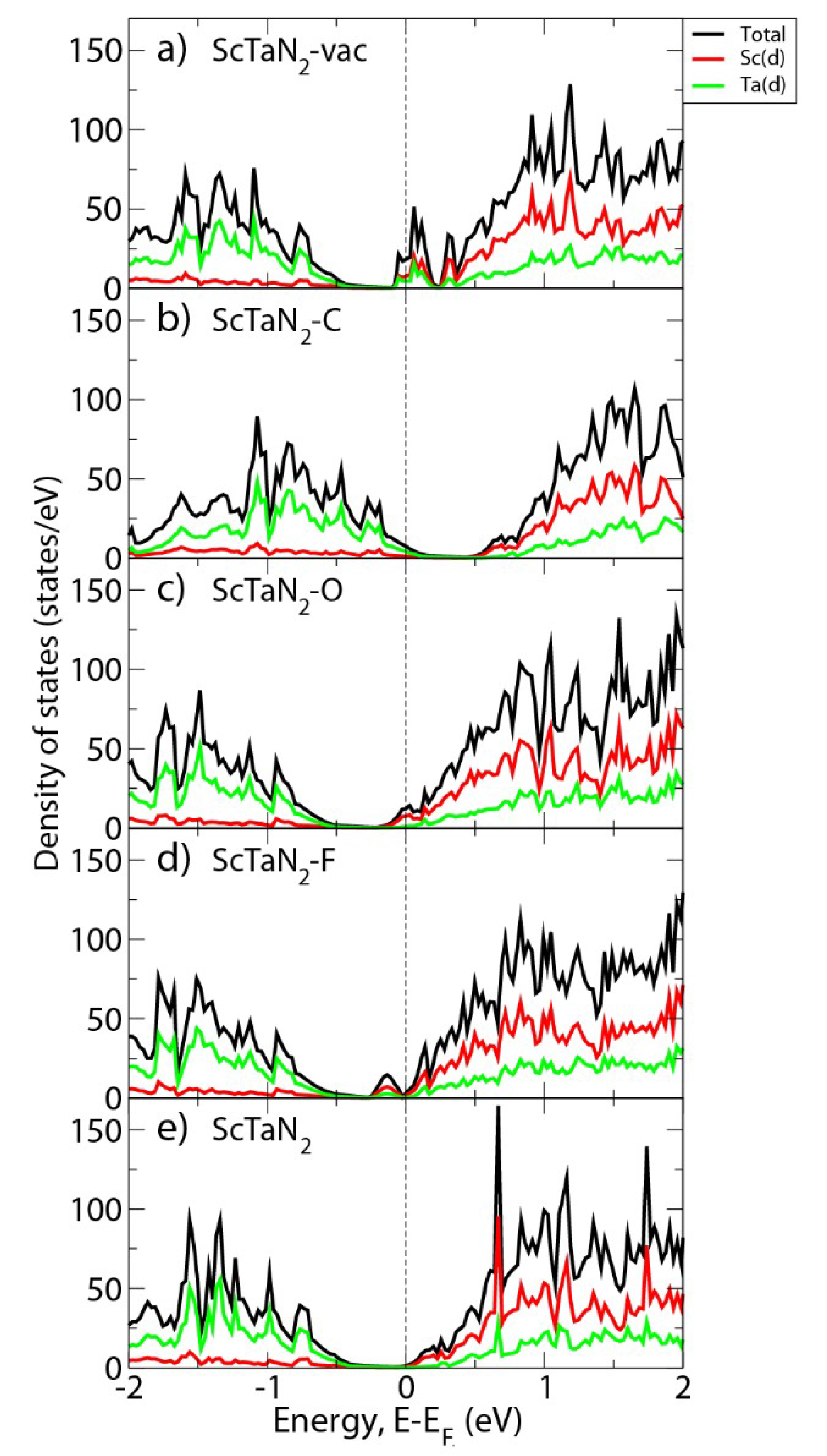
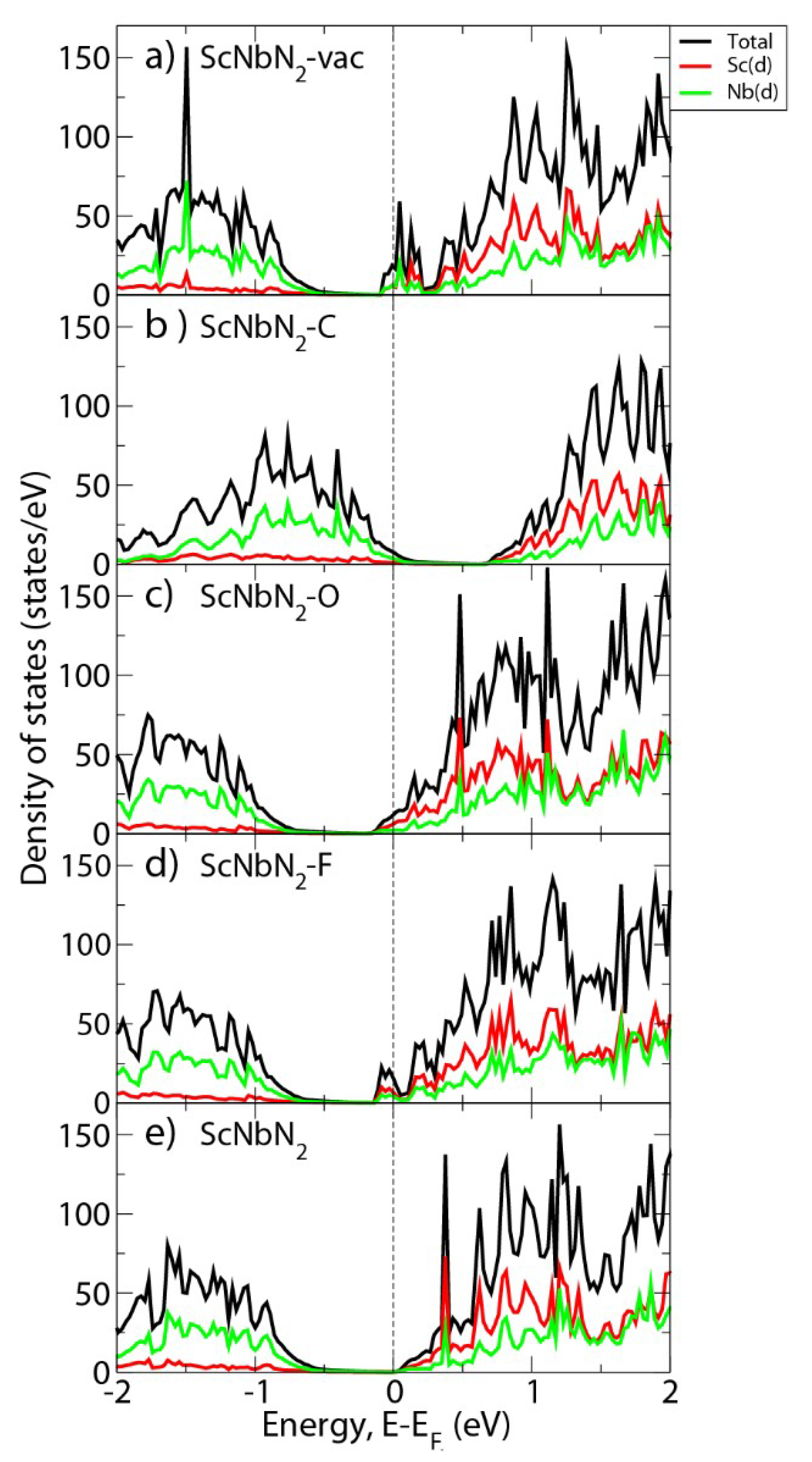
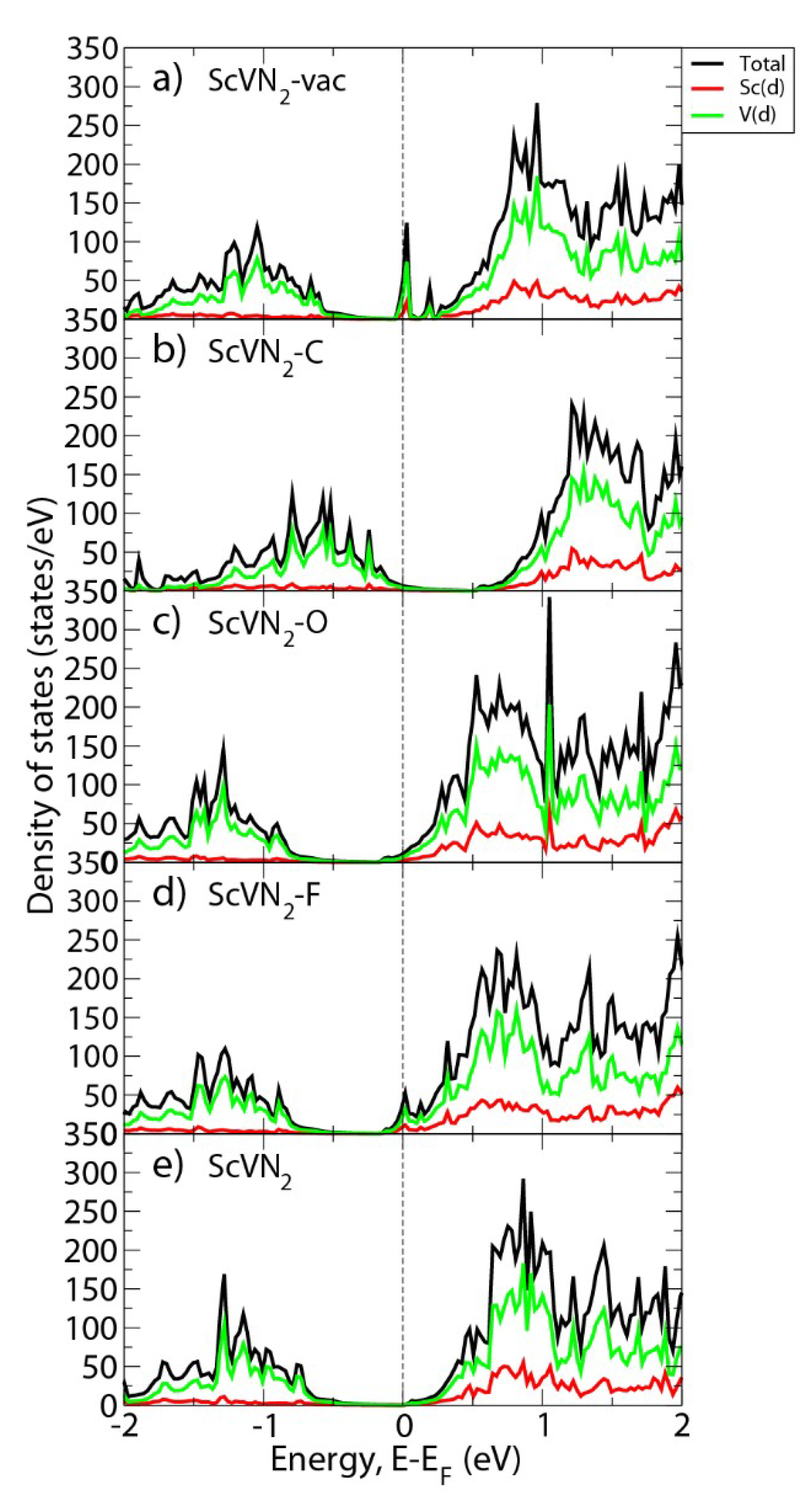
3. Results and Discussion

Table 1 shows the calculated defect formation energies of one vacancy or one C, O, or F dopant in ScTaN2, ScNbN2, and ScVN2. In the case of a vacancy to form, it can be noted that energy was needed for a single vacancy to form in all three systems. The case of one C dopant to be introduced also requires energy, but it can be noted that the formation energies were lower for all three systems compared to one vacancy. In contrast, for one O dopant to be incorporated, the formation energies were negative for all three systems. Here, it should be noted that the comparison included nitrogen or oxygen gas. Because O2 is a much more reactive molecule than N2, it is not surprising that substitutional inclusion of oxygen into the structures was preferred, especially as the O and N atoms still share many similarities when incorporated in solids in terms of open orbitals and atomic size. Finally, in the case of one F dopant to be introduced, it can be noted that the formation energies were positive in the cases of ScTaN2 and ScNbN2. In the case of ScVN2, the formation energy was negative, but close to zero. A similar argument about reactivity as for O above could be made for fluorine. However, the higher valence of F made it less favorable for incorporation into the nitride structure than O. Thus, the formation energy was found to be positive or only slightly negative.
Figure 1, Figure 2 and Figure 3 show the calculated total electronic DOS and projected DOS of stoichiometric ScTaN2, ScNbN2, and ScVN2 together with the DOS and projected DOS of the defect cases. In each figure, the bottom plot is the DOS of stoichiometric ScMN2. The other DOS curves of each figure are the DOS in the same system with a F, O, C, or F dopant or a vacancy, marked ScMN2-F, ScMN2-O, ScMN2-C, and ScMN2-vac. The energy of each individual DOS plot is adjusted so that the 0 eV corresponds to the highest occupied state. DOS far from the bandgaps are not included, as only features near the bandgaps affect electronic and thermoelectric properties.
In the stochiometric case, we have previously shown with the Heyd–Scuseria–Ernzerhof hybrid functional (HSE06) [22] that all three materials are semiconductors [22], consistent with experimental data on ScTaN2 [28]. Thus, in Figure 1, Figure 2 and Figure 3, the bandgaps are underestimated, because the DOS are calculated with GGA-PBE. It is well known that this approximation tends to underestimate bandgaps when compared to experimentally measured bandgaps [40]. Here, the purpose is to report changes and trends in the DOS due to point defects rather than give accurate bandgaps. Therefore, the underestimation of the bandgaps is not a concern, because the changes of the DOS are still being captured if the same exchange–correlation functional is used in all cases.
Figure 1a shows the DOS of the case of a single point vacancy in ScTaN2. Compared to the stoichiometric case in Figure 1e, the main difference is that in the defect case, an asymmetric peak feature is introduced at the highest occupied state. The asymmetric peak feature is an overlap between Sc 3d states and Ta 5d states. In the stochiometric case, there is a narrow peak with a high number of states, which cannot be seen in the vacancy case. This peak originates from Sc 3d states. Figure 1b shows the DOS in the case a single C dopant in ScTaN2. The main difference is that the highest occupied state has shifted into the valence band and that the Sc 3d state in the lower range of the conduction band in Figure 1e has disappeared. Figure 1c shows the DOS in the case of a single O dopant in ScTaN2. The highest occupied state has shifted into the conduction band and the Sc 3d state peak in the lower range of the conduction band in Figure 1e has disappeared. Figure 1d shows the DOS in the case of a single F dopant in ScTaN2. It can be noted that the highest occupied state has shifted into the conduction band and here it can be observed that the Sc 3d state peak in the lower range of the conduction band in Figure 1e has disappeared. It can also be noted that there is a new peak close the highest occupied state compared to Figure 1e. This peak mostly originates from Sc 3d states.
Figure 2a shows the DOS of the case of a single point vacancy in ScNbN2. When compared to the stoichiometric case in Figure 2e, it can be observed that there is a narrow peak with a high amount of states in the valence band, that there is a new asymmetric peak feature close to the highest occupied state, and that the narrow peak with a high number of states in the conduction band has disappeared. The first mentioned peak is due to Nb 4d states. The asymmetric peak close to the highest occupied state is mainly due to Sc 3d states. The peak in Figure 2e that originates from 3d states has disappeared. Figure 2b shows the DOS in the case of a single C dopant in ScNbN2. The narrow peak with high states in the conduction band has disappeared in Figure 1e. It can also be seen when compared to Figure 1e that the highest occupied state has shifted into the valence band. Figure 2c shows the DOS in the case of a single O dopant in ScNbN2. The main difference when compared to Figure 2e is that the highest occupied state has shifted into the conduction band. Figure 2d shows the DOS in the case of a single F dopant in ScNbN2. It can be noted that the narrow peak with a high number of states in Figure 2e has disappeared and that there is a new peak feature close to the highest occupied state. The latter peak is mostly due to Sc 3d states.
Figure 3a shows the DOS in the case of a single point vacancy in ScVN2. The main difference when compared to the stoichiometric case in Figure 3e is that there are two new sharp peaks close to the highest occupied state. These peaks originate mostly from V 3d states. Figure 2b shows the DOS in the case of a single C dopant in ScVN2. It can be observed that the highest occupied state has shifted into the valence band. Figure 3c shows the DOS in the case of a single O dopant in ScVN2. In the conduction band, a new sharp peak can be seen. This is due to V 3d states. It can also be noted that the highest occupied state has shifted into the conduction band. Figure 3d shows the DOS in the case of a single F dopant in ScVN2. Close the highest occupied state, a small peak feature that is due to V 3d states can be seen. Furthermore, the highest occupied state has shifted into the conduction band. If the DOS of a single F dopant in ScVN2 in Figure 3d is compared to the cases of a single F dopant in ScTaN2 and ScNbN2 in Figure 1d and Figure 2d, it can be remarked that the maximum of the peak feature close the highest occupied state in Figure 3d is located exactly at the highest occupied state. In Figure 1d and Figure 2d, the maxima of the corresponding peaks are located at lower energies than the highest occupied state. A local maximum in the DOS close the Fermi level is to a first approximation often correlated to a degree of structural instability, because a dip corresponds to a separation between bonding and antibonding states [31], which is consistent with the earlier conclusion that ScVN2 is a less stable system than ScTaN2 or ScNbN2 [22].
In terms of the transport distribution function, it has been theoretically shown that for a given lattice thermal conductivity, ZT is maximized when the transport distribution function consists of a Dirac delta function just above or below the Fermi level [41]. This is an idealized situation that does not correspond to real materials, but still a narrow distribution around the Fermi level will increase ZT [41,42]. If the transport distribution function is dominated by the DOS, the condition for maximizing ZT is translated into the presence of a sharp and narrow peak in the DOS close to the Fermi level [10,41]. For example, in a standard thermoelectric material such as PbTe, doping with Tl added additional energy levels close to the Fermi level and resulted in a doubling of the ZT value compared to Na-doped PbTe [10]. In Figure 1a, Figure 2a, and Figure 3a, where the N vacancy cases of ScTaN2, ScNbN2, and ScVN2 are presented, the vacancy introduced features close to the highest occupied state. Thus, a single vacancy should cause an increase in ZT compared to the stochiometric case. In particular, in the case of ScVN2, the increase is expected to be the most pronounced, because the peak feature in Figure 3a close the highest occupied state is sharper than in the two other cases in Figure 1a and Figure 2a.
Figure 1b, Figure 2b, and Figure 3b show that the highest occupied state is shifted into the valence band. ScTaN2, ScNbN2, and ScVN2 are in these figures p-doped with one C atom substituting for N. Saha et al. [21] reported that the alloying of ScN with Mg has the same effect on the Fermi level at 800 K, when the alloy composition resulted in a p-type material. It has also been shown that the Fermi level shifts towards the conduction band when the materials are doped with O. A study with Mg ion implantation with higher oxygen content retained n-type behavior [43]. Furthermore, it was noted in Figure 1c,d, Figure 2c,d, and Figure 3c,d that the highest occupied state is shifted into the conduction band in ScTaN2, ScNbN2, and ScVN2. These were doped with either O or F and the common factor is that these were all n-doped.
Calculations of Seebeck tensor components and ultimately ZT of the used supercells would be computationally expensive and would only give qualitative information, because the scattering time is unknown. In a previous paper, we however reported calculated transport properties of stoichiometric ScTaN2, ScNbN2, and ScVN2 as functions of chemical potential [22] that is here used to discuss the thermoelectric behavior of the dopant cases. All three systems are anisotropic. Therefore, the Sxx and Szz and tensor components as well as the ratio of σxx and σzz tensor components to the relaxation time τ were reported. In the present work, the shift of the highest occupied state compared to the stoichiometric cases is larger for the dopant cases than the vacancy cases. In the C dopant cases in Figure 1b, Figure 2b, and Figure 3b, the highest occupied state is shifted to the valence band, or in other words, the chemical potential was lowered. This should initially decrease the absolute values of the Sxx and Szz components of ScNbN2 and ScVN2 followed by a sign reversal, while the change of these components is expected to be less pronounced for ScTaN2. For σxx/τ, the shift to the conduction band is expected to lead to an increase of these values for all three systems. In the O and F dopant cases in Figure 1c,d, Figure 2c,d, and Figure 3c,d, the shift of the highest occupied state to the conduction band is observed, or in other words, the chemical potential increased. A very slight increase of chemical potential leads to a little decrease of |Sxx| and |Szz|, while a higher shift about the order of shift of O and F-doped ScTaN2, ScNbN2, and ScVN2 is expected to lead to an increase of both |Sxx| and |Szz| in all three cases.
For completeness, we also investigated the stability of the (hypothetical) phases YTaN2, YNbN2, and YVN2, i.e., with Sc replaced by an element in the same group of the periodic table (yttrium). These phases turned out to have a distorted structure of the ScTaN2-type structure. The formation enthalpies of these distorted YTaN2, YNbN2, and YVN2 structures with respect to the binaries were 0.259, −0.505, and 0.664 eV per formula unit. Thus, it can be concluded that only the distorted YNbN2 is expected to be thermodynamically stable. The structure parameters of the relaxed YNbN2 is presented in Table 2. It can be noted that the distortion is along the c-axis.

4. Conclusions

We used DFT calculations to investigate formation energies and the DOS of ScTaN2, ScNbN2, and ScVN2 when a nitrogen atom in the structure is replaced by a single vacancy or one C, O, or F dopant. The formation energies indicate that for all three systems, it costs energy to incorporate one vacancy or one C vacancy, while O incorporation corresponds to an energy gain, if the reaction products include the gaseous phases of nitrogen and oxygen. To incorporate one F atom into ScTaN2 and ScNbN2 also costs energy, while there is a gain of energy when F is incorporated into ScVN2, if the reaction products include the gaseous phases of nitrogen and fluorine. In the DOS, asymmetric peak features close to the highest occupied state is the result of incorporating one vacancy in three phases, which is expected to increase ZT. Furthermore, one C dopant in ScTaN2, ScNbN2, and ScVN2 implies a shift of the highest occupied state into the valence band, while one O or F dopant implies a shift of the highest occupied state into the conduction band. In conclusion, this study shows that there is a promising pathway to tune the thermoelectric properties and to increase the figure of merit of the three studied ScTaN2, ScNbN2, and ScVN2 material systems.

Author Contributions

Conceptualization, P.E. and S.S.; Supervision, P.E. and S.S.; Software and computational design, R.P.; Formal Analysis, R.P.; Writing-Original Draft Preparation, R.P.; Writing-Review & Editing, P.E., R.P. and S.S.; Visualization, R.P.; Project Administration, R.P.; Funding Acquisition, P.E. and S.S.

Funding

The authors acknowledge support from the Swedish Research Council (VR) through project grant number 2016-03365, the Knut and Alice Wallenberg Foundation through the Wallenberg Academy Fellows program, and the Swedish Government Strategic Research Area in Materials Science on Functional Materials at Linköping University (Faculty Grant SFO-Mat-LiU No. 2009 00971).

Acknowledgments

The calculations were performed using computer resources provided by the Swedish National Infrastructure for Computing (SNIC) at the National Supercomputer Centre (NSC). We would also like to thank Weine Olovsson at NSC and Björn Alling at IFM for very useful help with the calculations.

Conflicts of Interest

The authors declare no conflict of interest.

References

  1. Sun, R.; Wang, Z.; Saito, M.; Shibata, N.; Ikuhara, Y. Atomistic mechanisms of nonstoichiometry-induced twin boundary structural transformation in titanium dioxide. Nat. Commun. 2015, 6, 7120. [Google Scholar] [CrossRef] [PubMed]
  2. Van de Walle, C.G.; Neugebauer, J. First-principles calculations for defects and impurities: Applications to III-nitrides. J. Appl. Phys. 2004, 95, 3851. [Google Scholar] [CrossRef]
  3. Wang, Z.; Saito, M.; McKenna, K.P.; Gu, L.; Tsukimoto, S.; Shluger, A.L.; Ikuhara, Y. Atom-resolved imaging of ordered defect superstructures at individual grain boundaries. Nature 2011, 479, 380–383. [Google Scholar] [CrossRef] [PubMed]
  4. Kerdsongpanya, S.; Alling, B.; Eklund, P. Effect of point defects on the electronic density of states of ScN studied by first-principles calculations and implications for thermoelectric properties. Phys. Rev. B 2012, 86, 195140. [Google Scholar] [CrossRef] [Green Version]
  5. Ma, D.; Ju, W.; Tang, Y.; Chen, Y. First-principles study of the small molecule adsorption on the InSe monolayer. Appl. Surf. Sci. 2017, 426, 244–252. [Google Scholar] [CrossRef]
  6. Wang, Z.; Tsukimoto, S.; Saito, M.; Ikuhara, Y. SiC/Ti3SiC2 interface: Atomic structure, energetics, and bonding. Phys. Rev. B 2009, 79, 045318. [Google Scholar] [CrossRef]
  7. Eklund, P.; Kerdsongpanya, S.; Alling, B. Transition-metal-nitride-based thin films as novel energy harvesting materials. J. Mater. Chem. C 2016, 4, 3905–3914. [Google Scholar] [CrossRef] [PubMed] [Green Version]
  8. Li, J.-F.; Liu, W.-S.; Zhao, L.-D.; Zhou, M. High-performance nanostructured thermoelectric materials. NPG Asia Mater. 2010, 2, 152–158. [Google Scholar] [CrossRef]
  9. Dresselhaus, M.S.; Chen, G.; Tang, M.Y.; Yang, R.G.; Lee, H.; Wang, D.Z.; Ren, Z.F.; Fleurial, J.-P.; Gogna, P. New Directions for Low-Dimensional Thermoelectric Materials. Adv. Mater. 2007, 19, 1043–1053. [Google Scholar] [CrossRef]
  10. Heremans, J.P.; Jovovic, V.; Toberer, E.S.; Saramat, A.; Kurosaki, K.; Charoenphakdee, A.; Yamanaka, S.; Snyder, G.J. Enhancement of Thermoelectric Efficiency in PbTe by Distortion of the Electronic Density of States. Science 2008, 321, 554–557. [Google Scholar] [CrossRef] [PubMed] [Green Version]
  11. Biswas, B.; Saha, B. Development of semiconducting ScN. Phys. Rev. Mater. 2019, 3, 020301. [Google Scholar] [CrossRef]
  12. Kerdsongpanya, S.; Alling, B.; Eklund, P. Phase stability of ScN-based solid solutions for thermoelectric applications from first-principles calculations. J. Appl. Phys. 2013, 114, 073512. [Google Scholar] [CrossRef] [Green Version]
  13. Kerdsongpanya, S.; Sun, B.; Eriksson, F.; Jensen, J.; Lu, J.; Koh, Y.K.; Nong, N.V.; Balke, B.; Alling, B.; Eklund, P. Experimental and theoretical investigation of Cr1−xScxN solid solutions for thermoelectrics. J. Appl. Phys. 2016, 120, 215103. [Google Scholar] [CrossRef]
  14. Saha, B.; Garbrecht, M.; Perez-Taborda, J.A.; Fawey, M.H.; Koh, Y.R.; Shakouri, A.; Martin-Gonzalez, M.; Hultman, L.; Sands, T.D. Compensation of native donor doping in ScN: Carrier concentration control and p-type ScN. Appl. Phys. Lett. 2017, 110, 252104. [Google Scholar] [CrossRef]
  15. Tureson, N.; Van Nong, N.; Fournier, D.; Singh, N.; Acharya, S.; Schmidt, S.; Belliard, L.; Soni, A.; Eklund, P. Reduction of the thermal conductivity of the thermoelectric material ScN by Nb alloying. J. Appl. Phys. 2017, 122, 025116. [Google Scholar] [CrossRef] [Green Version]
  16. Rawat, V.; Koh, Y.K.; Cahill, D.G.; Sands, T.D. Thermal conductivity of (Zr,W)N/ScN metal/semiconductor multilayers and superlattices. J. Appl. Phys. 2009, 105, 024909. [Google Scholar] [CrossRef]
  17. Saha, B.; Koh, Y.R.; Comparan, J.; Sadasivam, S.; Schroeder, J.L.; Garbrecht, M.; Mohammed, A.; Birch, J.; Fisher, T.; Shakouri, A.; et al. Cross-plane thermal conductivity of (Ti,W)N/(Al,Sc)N metal/semiconductor superlattices. Phys. Rev. B. 2016, 93, 45311. [Google Scholar] [CrossRef] [Green Version]
  18. Schroeder, J.L.; Saha, B.; Garbrecht, M.; Schell, N.; Sands, T.D.; Birch, J. Thermal stability of epitaxial cubic-TiN/(Al,Sc)N metal/semiconductor superlattices. J. Mater. Sci. 2015, 50, 3200–3206. [Google Scholar] [CrossRef] [Green Version]
  19. Zebarjadi, M.; Bian, Z.; Singh, R.; Shakouri, A.; Wortman, R.; Rawat, V.; Sands, T. Thermoelectric Transport in a ZrN/ScN Superlattice. J. Electron. Mater. 2009, 38, 960–963. [Google Scholar] [CrossRef] [Green Version]
  20. Gharavi, M.A.; Kerdsongpanya, S.; Schmidt, S.; Eriksson, F.; Nong, N.V.; Lu, J.; Balke, B.; Fournier, D.; Belliard, L.; le Febvrier, A.; et al. Microstructure and thermoelectric properties of CrN and CrN/Cr2N thin films. J. Phys. D 2018, 51, 355302. [Google Scholar] [CrossRef]
  21. Saha, B.; Perez-Taborda, J.A.; Bahk, J.-H.; Koh, Y.R.; Shakouri, A.; Martin-Gonzalez, M.; Sands, T.D. Temperature-dependent thermal and thermoelectric properties of n-type and p-type Sc1−xMgxN. Phys. Rev. B 2018, 97, 085301. [Google Scholar] [CrossRef]
  22. Pilemalm, R.; Pourovskii, L.; Mosyagin, I.; Simak, S.; Eklund, P. Thermodynamic Stability, Thermoelectric, Elastic and Electronic Structure Properties of ScMN2-Type (M = V, Nb, Ta) Phases Studied by ab initio Calculations. Condens. Matter 2019, 4, 36. [Google Scholar] [CrossRef]
  23. Lengauer, W. The crystal structure of ScNbN1−x and comparisons with related nitride and carbide structures. J. Solid State Chem. 1989, 82, 186–191. [Google Scholar] [CrossRef]
  24. Lengauer, W.; Ettmayer, P. The Crystal Structure of ScTaN1−x. J. Less Common Met. 1988, 141, 157–162. [Google Scholar] [CrossRef]
  25. Burmistrova, P.V.; Maassen, J.; Favaloro, T.; Saha, B.; Salamat, S.; Rui Koh, Y.; Lundstrom, M.S.; Shakouri, A.; Sands, T.D. Thermoelectric properties of epitaxial ScN films deposited by reactive magnetron sputtering onto MgO(001) substrates. J. Appl. Phys. 2013, 113, 153704. [Google Scholar] [CrossRef] [Green Version]
  26. Burmistrova, P.V.; Zakharov, D.N.; Favaloro, T.; Mohammed, A.; Stach, E.A.; Shakouri, A.; Sands, T.D. Effect of deposition pressure on the microstructure and thermoelectric properties of epitaxial ScN(001) thin films sputtered onto MgO(001) substrates. J. Mater. Res. 2015, 30, 626–634. [Google Scholar] [CrossRef] [Green Version]
  27. Le Febvrier, A.; Tureson, N.; Stilkerich, N.; Greczynski, G.; Eklund, P. Effect of impurities on morphology, growth mode, and thermoelectricproperties of (1 1 1) and (0 0 1) epitaxial-like ScN films. J. Phys. D Appl. Phys. 2019, 52, 035302. [Google Scholar] [CrossRef]
  28. Niewa, R.; Zherebtsov, D.A.; Schnelle, W.; Wagner, F.R. Metal−Metal Bonding in ScTaN2. A New Compound in the System ScN−TaN. Inorg. Chem. 2004, 43, 6188–6194. [Google Scholar] [CrossRef]
  29. Barsoum, M.W. The MN+1AXN phases: A new class of solids; thermodynamically stable nanolaminates. Prog. Solid State Chem. 2000, 28, 201–281. [Google Scholar] [CrossRef]
  30. Barsoum, M.W. The MAX phases: Unique new carbide and nitride materials. Am. Sci. 2001, 89, 334. [Google Scholar] [CrossRef]
  31. Eklund, P.; Beckers, M.; Jansson, U.; Högberg, H.; Hultman, L. The Mn + 1AXn phases: Materials science and thin-film processing. Thin Solid Films 2010, 518, 1851–1878. [Google Scholar] [CrossRef]
  32. Kresse, G.; Furtmüller, J. Efficient iterative schemes for ab initio total-energy calculations using a plane wave basis set. Phys. Rev. B 1996, 54, 11169. [Google Scholar] [CrossRef] [PubMed]
  33. Kresse, G.; Furtmüller, J. Efficiency of ab-initio total energy calculations for metals and semiconductors using a plane-wave basis set. Comput. Mater. Sci. 1996, 6, 15–50. [Google Scholar] [CrossRef]
  34. Kresse, G.; Hafner, J. Ab initio molecular dynamics for liquid metals. Phys. Rev. B Condens. Matter Mater. Phys. 1993, 47, 558–561. [Google Scholar] [CrossRef] [PubMed]
  35. Kresse, G.; Hafner, J. Ab initio molecular-dynamics simulation of the liquid-metal-amorphous-semiconductor transition in germanium. Phys. Rev. B Condens. Matter Mater. Phys. 1994, 49, 14251–14269. [Google Scholar] [CrossRef] [PubMed]
  36. Kohn, W.; Sham, L.J. Self-Consistent Equations Including Exchange and Correlation Effects. Phys. Rev. 1965, 140, A1133. [Google Scholar] [CrossRef]
  37. Blöchl, P.E. Projector augmented-wave method. Phys. Rev. B 1994, 50, 17953–17979. [Google Scholar] [CrossRef] [PubMed] [Green Version]
  38. Perdew, J.P.; Burke, F.; Ernzerhof, M. Generalized Gradient Approximation Made Simple. Phys. Rev. Lett. 1996, 77, 3865–3868. [Google Scholar] [CrossRef] [Green Version]
  39. Blöchl, P.E.; Jepsen, O.; Andersen, O.K. Improved tetrahedron method for Brillouin-zone integrations. Phys. Rev. B 1994, 49, 16223. [Google Scholar] [CrossRef]
  40. Bagayoko, D. Understanding density functional theory (DFT) and completing it in practice. AIP Adv. 2014, 4, 127104. [Google Scholar] [CrossRef] [Green Version]
  41. Mahan, G.D.; Sofo, J.O. The best thermoelectric. Proc. Natl. Acad. Sci. USA 1996, 93, 7436–7439. [Google Scholar] [CrossRef] [PubMed]
  42. Fan, Z.; Wang, H.-Q.; Zheng, J.-C. Searching for the best thermoelectrics through the optimization of transport distribution function. J. Appl. Phys. 2011, 109, 073713. [Google Scholar] [CrossRef]
  43. Tureson, N.; Marteau, M.; Cabioch, T.; Van Nong, N.; Jensen, J.; Lu, J.; Greczynski, G.; Fournier, D.; Singh, N.; Soni, A.; et al. Effect of ion-implantation-induced defects and Mg dopants on the thermoelectric properties of ScN. Phys. Rev. B 2018, 98, 205307. [Google Scholar] [CrossRef] [Green Version]
Figure 1. DOS and DOS projections of ScTaN2 for the single point defect, (a) vacancy, (b) C-doped, (c) O-doped, (d) F-doped; as well for the (e) stoichiometric case.
Condensedmatter 04 00070 g001
Figure 2. DOS and DOS projections of ScNbN2 for the single point defect, (a) vacancy, (b) C-doped, (c) O-doped, (d) F-doped; as well for the (e) stoichiometric case.
Condensedmatter 04 00070 g002
Figure 3. DOS and DOS projections of ScVN2 for the single point defect, (a) vacancy, (b) C-doped, (c) O-doped, (d) F-doped; as well for the (e) stoichiometric case.
Condensedmatter 04 00070 g003
Table 1. Formation energies of defects, i.e., one vacancy or one dopant of ScTaN2, ScNbN2, or ScVN2.
M in ScMN2Ef(vac) of ScMN2
(eV)
Ef(C) of ScMN2 (eV)Ef(O) of ScMN2 (eV)Ef(F) of ScMN2 (eV)
Ta1.911.67−1.041.13
Nb2.961.82−1.210.79
V2.141.86−1.48−0.06
Table 2. Structure parameters of the YNbN2 structure.
Parameter
a (Å)3.1805
b (Å)3.1805
c (Å)11.1095
α90.0°
β90.0°
γ119.4°

