Abstract
The article presents the results of an experimental study of the transport of charge carriers through semiconductor PANI-polystyrene/ ferroelectric PVDF-TrFE interface. Current-voltage characteristics of the structure under study have a typical form for memristors and may be explained by the movement of charge carriers in the internal switchable field of the crystal ferroelectric microregions located within a bulk volume of amorphous PVDF-TrFE matrix. This assumption is subject to XRD phase analysis, FTIR spectroscopy, and X-ray EDS microanalysis. A long-term (about 100 h) relaxation is detected for the resistance of the PANI-polysturene/PVDF-TrFE interface after the current-voltage characteristics measurement cycle that is associated with the processes of capture and release traps of charge carriers.
1. Introduction
Nowadays, the development of organic electronics intensifies research in the field of obtaining and studying properties of new types of composite materials, which combine conductive, semiconductor, and dielectric polymers (including piezo- and ferroelectrics) [1]. At the same time, the actual performances of polymer electronics devices are still significantly inferior to conventional silicon devices. However, for some types of devices, for instance, memristors, for polymer devices, the operation speed comparable with inorganic analogues has been achieved [2]. Since these devices have significantly higher biocompatibility, they present considerable interest referring to the creation of analogue neuromorphic computers based on crossbar architectures [3].
Recently, several types of memristor elements are implemented on the basis of polymeric materials and their composites. The most distinguishing examples are: polyaniline (PANI) memristor based on the conductivity changes due to chemical reactions of oxidation and reduction [4], poly(vinylidene fluoride-trifluoroethylene) PVDF–TrFE/ poly(methyl methacrylate) (PMMA) blended films memristor based on the switching of ferroelectric polarization [5], poly(3-hexylthiophene) P3HT/PVDF-TrFE with ferroelectric polarization field, which modules the injection barrier at the semiconductor–metal contact [6]. It is known that the dipole orientation on the interface “ferroelectric polymer–conductive polymer” such as PVDF-TrFE/poly(3,4-ethylenedioxythiophene): polystyrene sulfonate (PEDOT:PSS) increases the free carrier extraction yield by supporting the internal field of the polymer interface [7]. It is shown that the polarization switching of the ferroelectric polymer leads to high nonlinearity and bistability in ion-doped conducting polymers [8]. Moreover, Ref. [9] demonstrates unique features of phase separated blend ferroelectric PVDF-TrFE/semiconductor poly(9,9-dioctylfluorene) (PFO) organic ferroelectric diodes as memory cells. In this case, the ferroelectric polarization switching allows controlling tunneling through the interface by modulating the width of the energy barrier. In addition, it leads to the polarization resulting in a formation of the strongly accumulated hole density along the whole interface between the PFO and PVDF-TrFE, i.e., the mobility increases with the charge carrier density.
All polymer composite materials of the type “semiconductor PANI (emeraldine salt)/ferroelectric PVDF-TrFE” cause widespread interest for their use as materials for developing heterojunction diodes [10], organic ferroelectric memory devices [11], flexural piezo-FET and nanogenerators [12]. The heterojunction formation is expected from the band offsets of two polymers near the Fermi level. For this type of heterojunctions, a characteristic abrupt interface of electron states is their typical feature [10]. It is reported in the paper [12] that the charge transport modulation occurs due to the strain-induced conformational changes in PVDF-TrFE leading to the changes in the carrier localization–delocalization. Under the application of flexural strain, the polarization in PVDF-TrFE increases. This leads to electrostatic interactions between electronegative fluorine and hydrogen of PANI. This property provides delocalizing carriers in PANI. Due to this interaction, nitrogen becomes electron donating and the electron cloud gets pulled by an adjacent benzene ring resulting in an efficient delocalization. However, unlike the structures considered earlier (P3HT/PVDF-TrFE, PVDF-TrFE/(PEDOT:PSS), PVDF-TrFE/PFO), for these interfaces, the question of the influence of the ferroelectric polarization and its switching on the transport of charge carriers has not been sufficiently considered yet. Thus, the principal goal of this work is a detailed experimental study of nonlinear conductivity effects on the PVDF-TrFE/PANI-polystyrene interface.
2. Materials and Methods
2.1. Materials
PVDF-TrFE (Sigma-Aldrich, Solvene®300) was dissolved in acetone in 5 wt%. The solution was stirred for three hours with a magnetic stirrer at 30 °C and, after this, was dropwise deposited on an aluminum foil and dried at the temperature of −10 °C during 24 h. Polyaniline (PANI) (emeraldine salt) (Sigma-Aldrich) (MW > 15,000, particle size 3–100 µm, surface area 5–20 m2/g, conductivity for compacted powder 2–4 S/cm) was added to 5 wt% solution. Polystyrene (PS) (Sigma-Aldrich) (average Mw 35,000) in toluene in the 15%/85% volume ratio. Since the commercially available PANI was used for the synthesis of samples, additive of polystyrene was used for increasing the flexibility and the mechanical strength of the films. To achieve homogeneity, the resulting suspension was dispersed by ultrasonic (23.5 kHz, 300 W, 5 min) for the volume of suspension 5 mL. The resulting solution was poured on top PVDF-TrFE film and for 24 h was placed in the freezer (−10 °C) to evaporate acetone. The electrodes were made by the silver paste coating.
Annealing of films is known to have a significant effect on their crystal structure [13]. Evaporation of acetone at the low temperature was performed for obtaining PVDF-TrFE film with a high content of amorphous phase, which should incorporate individual ferroelectric crystalline inclusions. Such a structure is widely known in PVDF-TrFE films [14]. At the same time, the electrical voltages required for switching individual crystallites are much smaller than for micrometer scale thickness films, as it will be estimated below.
2.2. Methods
Scanning electronic microscopy (SEM) images of interfaces profiles were obtained by TESCAN VEGA 3 LM (TESCAN, Chech Republic). The elemental composition of the interface surface was investigated by the method of energy-dispersive X-ray spectroscopy (EDS) (Bruker X-Flash, Bruker, USA).
Methods of X-ray diffraction (XRD) and infrared Fourier spectroscopy (FTIR) were used to characterize the structure of the obtained composite material. X-ray diffraction (XRD) pattern of the composite material (CuKα1 radiation, λ = 1.54056 Å) was obtained in the range 2θ of 10°–60° with the step scan 0.02° (15 min) using Bruker D8 Advance ECO diffractometer (Bruker, USA).
FTIR spectrum of the composite film was obtained in the absorbance mode (Nicolet iS-50, Thermo Fisher Scientific, USA) in the range 700–1500 cm−1.
For measuring current-voltage characteristics, the sample (with the initial resistance of 16 kOhm) was included in the voltage divider analogue circuit (the sample and the reference resistor 10 kOhm); Aktakom APS 3505 (Aktakom, Russia) was used as a voltage source. During each measuring cycle, bias voltages from 0 to 12 V and back were applied to the divider, then the polarity of the bias voltage was changed and the measurement process was repeated. For registering the voltage drop signal on the reference resistance the oscilloscope Agilent DSO X 2024A (Keysight Technologies, USA) was used.
For studying the long-term relaxation of the resistance, the sample was connected to the analogue input of the board according to the voltage divider circuit (the photoresistor and the reference resistor 10 kOhm). A ten-bit ADC and the reference voltage of 5 V were used to accurately track changes in the resistance of the sample. Every hour, the system took 1000 measurements from the analogue input and averaged them. The obtained data were recorded in the EEPROM microscheme AT24C256 series with the subsequent output to a computer via the serial port. When performing measurements, any sources of illumination were absent and ambient temperature was maintained at 20 °C.
3. Results
Figure 1 shows the SEM images of the obtained polymer PANI-PS/PVDF-TrFE composite material on the aluminum substrate. The ratio of the thickness of the layers PANI-PS (upper layer) and PVDF-TrFE (bottom layer) are equal to 60:30 μm. In addition, it should be noted that the layer PANI-PS has large porosity. The significant difference in the electrical conductivity of polymers makes it possible to clearly visualize the phase boundary (Figure 2a). However, the X-ray EDS analysis clearly demonstrates a presence of uncharacteristic elements (Fluorine in PANI-PS and sulfur for PVDF-TrFE) in the layers at distances up to 40 μm from the interface (Figure 2b,c). This fact emphasizes significant interlayer diffusion.
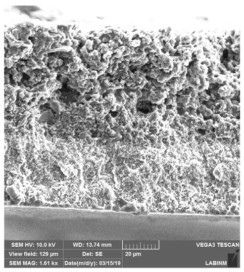
Figure 1.
SEM images of the obtained PVDF-TrFE/PANI-PS interface.
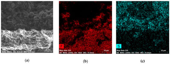
Figure 2.
SEM image of PANI-PS/PVDF-TrFE interface (a); elemental maps of fluorine (b) and sulfur (c) for this area (after 4 cycles of measuring current-voltage characteristics).
Figure 3 shows the diffraction pattern of the obtained PANI-PS/PVDF-TrFE composite film. The ratio of amorphous and crystalline phases in the obtained samples was 65:35. The peak at 19.4° corresponds to the overlapping of (110) and (200) reflections and can be attributed to the ferroelectric β phase of PVDF-TrFE [15]. Weak peaks 34.2° and 43.4° are caused by the presence of paraelectric α phase of PVDF-TrFE [16]. At the same time, broad amorphous halo indicate an existence PVDF-TrFE in the amorphous phase. Peaks 24.6°, 26.3° and 40.1° correspond to (005), (111) and (200) PANI reflexes in the pseudo-orthorhombic crystal phase [17].
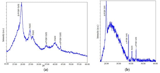
Figure 3.
XRD pattern of bilayer PANI-PS/PVDF-TrFE composite after (a) and before (b) 4 cycles of measuring current-voltage characteristics).
The pattern obtained for the sample after four measuring cycles current-voltage characteristics shows an increase in the intensity of the peaks associated with α phase of PVDF-TrFE, which originates from irradiation of X-ray [14]. However, there is no any decrease in the peak intensity 19.4° (β-PVDF-TrFE).
FTIR spectrum of the obtained composite material (Figure 4) demonstrates a presence of the peak splitting near 850 cm−1; the peaks 1285 and 1403 cm−1 also confirm the ferroelectric β crystalline phase of PVDF-TrFE [16,17]. The observed peaks 1155 and 1070 cm−1 characterize the conductive emeraldine salt form of PANI; the 1430 cm-1 band is typical for the emeraldine base form of PANI [18,19]. This fact testifies the partial protonation of emeraldine and confirms the semiconductor type of its electric conductivity.
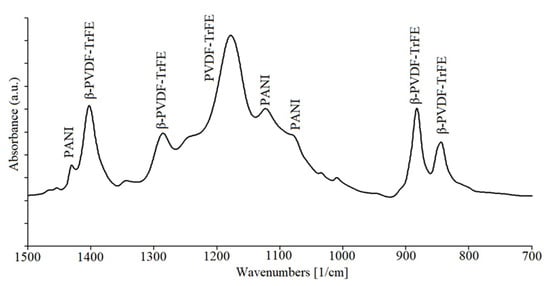
Figure 4.
FTIR spectrum of bilayer PANI-PS/PVDF-TrFE composite.
The current-voltage characteristic of the obtained bilayer structure is shown in the Figure 5a. In the area of positive bias voltage observed curves are similar with PANI/PVDF-TrFE heterojunction [10]. The hysteresis of the current-voltage characteristic observed in this case is due to an injection of carriers from the electrode to the trap site located in the interface between semiconductor-dielectric layers as well as in the case considered in [20].
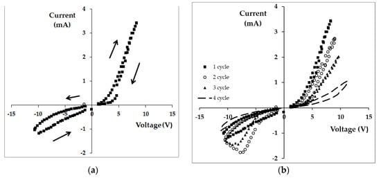
Figure 5.
Current-voltage characteristics of PVDF-TrFE/PANI-PS bilayer structure for the first cycle (a) and for a sequence of 4 cycles (the interval between cycles is equal to 24 h) that illustrates a degradation of current-voltage characteristics (b).
At the same time, the figure shows the evolution of the current-voltage characteristics of the structure under study during repeated cycles. In this case, the time interval between each cycle was 24 h. The intensity of the current through the interface drops with each cycle should be noted in this case. In the fourth measuring cycle, a hysteresis was observed in the current-voltage characteristics in addition to the intensive growth of the sample resistance.
Simultaneously, a number of differences exists for the area of negative bias voltages. First of all, it should be noted that for the structure under study, in contrast to the typical polymer heterojunction, the reverse currents are comparable in magnitude with the direct currents for all measurement cycles. Besides that, the hysteresis of the current-voltage characteristic exists in this case already on the first measurement cycle. Over the next 2 cycles, its area increases, and then (4 cycle) drastically reduces, coming to the symmetry with a view of the curves for the region of positive voltages. Thus, a decrease in the amplitude of the current-voltage characteristics with an increase in the number of measurement cycles may indicate the presence of long-term conduction relaxation in the sample under study.
Obtained data suggest that the resistance of the sample after the measurement cycle of the current-voltage characteristics does not return to its initial value within 24 h. For example, for a sample with the initial resistance of 16 kΩ, after measuring its current-voltage characteristics, the resistance was 32 kΩ (Figure 6). The resistance relaxes to its initial state in a time interval of about 100 h.
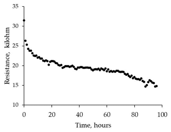
Figure 6.
Resistance relaxation of PVDF-TrFE/PANI-PS bilayer structure.
4. Discussion
First of all, we should discuss the presence of a hysteresis loop in I–V characteristic observed during the first three cycles of polarization switching for the region of negative bias voltages. It should be noted that this type of obtained dependences can be associated with a possible influence of the ferroelectric polarization of PVDF-TrFE Ref. [9] argues that tunneling is the main mechanism for the transport of charges through a similar barrier. At the same time, the PANI/PVDF-TrFE phase interface has an abrupt interface of electron states [10]. Thus, the application of a reverse bias voltage to such heterojunction can lead to polarization switching. Respectively, depending on the direction, this effect will increase or decrease the energy of the potential barrier located at the interface. However, in this case, polarization switching is possible only in individual PVDF-TrFE microregions. This possibility is confirmed by the analysis of diffraction patterns of the studied samples (Figure 4), according to which the PVDF-TrFE layer is an amorphous matrix filled with crystalline inclusions in the ferroelectric β phase, the characteristic lengths of which are estimated from the Debye–Scherer equation are ~60 nm. Thus, the magnitude of the applied field switching the polarization of the nanocrystals can be estimated as 2 MV/cm, which is close to the data obtained for P(VDF-TrFE) copolymer nanodots such sizes in [21]. Thus, the applied voltages are sufficient to switch the polarization in these microregions.
Further, it should be noted that a decrease in the magnitude of the current flowing through the interface with each subsequent measuring cycle. It can be caused by the processes of capturing charge carriers into traps formed by both impurity centers as a result of diffusion (Figure 2) and the “crystalline polarized region–amorphous matrix” interface in PVDF-TrFE. It is obvious that diffusion leads to a blurring of the phase boundary at which charge carriers accumulate (in the case of PANI holes) [9] that changes the mechanism of the charge carrier transport. The effect of a potential barrier on the transport of charge carriers through the interface is reduced due to the formation of a significant number of “random field” defects, which are also traps for charge carriers. This assumption is confirmed by the type of current-voltage characteristic obtained from the fourth measurement cycle. The current through the interface, in this case, is much smaller (due to the capture of carriers in the traps). In addition, this dependence is absolutely symmetric with respect to the polarity of the external voltage, and the existing hysteresis originates due to the processes of capture and release of charge carriers under an action of the external field. Since this diffusion process is irreversible, it leads to irreversible degradation of the memristive properties of the structure under study. Moreover, according to the EDS element maps, a phase blend is formed at the interphase. However, the observed hysteresis behavior can not originate from the Maxwell–Wagner effect (at least up to complete degradation of this composite material) due to sufficient asymmetry of current-voltage loops. As it discussed above, such asymmetry is directly connected with principal difference between processes generating half-loops: the carriers injection from the electrode to the trap (positive voltages) and the polarization switching of PVDF-TrFE nanocrystals (negative voltages).
These processes also determine the long-term relaxation of the resistance (Figure 6) observed for the interface. External bias voltages applied during the measurement cycles of the current-voltage characteristics result in the charge redistribution on carrier traps and their subsequent emptying.
Thus, memristive properties of the structure under study emerge due to the both polarization switching processes and the capture and release of charge carriers from traps localized near the interface. At the same time, diffusion leads to the formation of a blend at the phase boundaries with increasing number of measurement cycles. Since the interface (abrupt interface of electron states) degrades, it becomes impossible to apply an external voltage sufficient to switch the polarization of ferroelectric crystallites. Therefore, with an increase in the number of cycles, the hysteresis of the current–voltage characteristics of the structure becomes to exist only due to the processes of capture and release of carriers from traps. This leads to a symmetric shape of the I–V hysteresis.
5. Conclusions
Analysis of the experimental results allows the following conclusions:
- Two-layer PANI-polystyrene/PVDF-TrFE polymer composite material with memristor-like current-voltage characteristics due to the structural features of the PVDF-TrFE layer (crystalline ferroelectric inclusions in an amorphous matrix) and diffusion of charged impurities through the interface was obtained;
- Resulting composite material has a hysteresis of current-voltage characteristics due to the polarization switching processes in the PVDF-TrFE microregions, as well as the capture and release of charge carriers from various types of traps;
- During the measuring cycles, the form of the current-voltage characteristics changes substantially that is caused by structural changes at the interface;
- Due to the described processes, the resulting composite material has a long-term (about 100 h) relaxation resistance.
Author Contributions
All authors contributed equally to prepare the experiments, propose the mechanisms involved, and analyze the results.
Funding
This research was funded by the Russian Science Foundation, grant number 18-72-00148.
Acknowledgments
The authors are grateful to E.B. Postnikov (Kursk State University) and L.N. Korotkov (Voronezh State Technical University) for a fruitful discussion of this research.
Conflicts of Interest
The authors declare no conflict of interest.
References
- Silva, S.R.P.; Beliatis, M.J.; Jayawardena, K.D.G.I.; Mills, C.A.; Rhodes, R.; Rozanski, L.J. Hybrid and nanocomposite materials for flexible organic. In Handbook of Flexible Organic Electronics. Materials, Manufacturing and Application, 1st ed.; Logothetidis, S., Ed.; Woodhead Publishing: Cambridge, UK, 2014; pp. 57–74. [Google Scholar]
- Valov, I.; Kozicki, M. Organic memristors come of age. Nat. Mater. 2017, 16, 1170–1172. [Google Scholar] [CrossRef] [PubMed]
- Pecqueur, S.; Vuillaume, D.; Alibart, F. Perspective: Organic electronic materials and devices for neuromorphic engineering. J. Appl. Phys. 2018, 124, 151902. [Google Scholar] [CrossRef]
- Demin, V.A.; Erokhin, V.V.; Emelyanov, A.V.; Battistoni, S.; Baldi, G.; Iannotta, S.; Kashkarov, P.K.; Kovalchuk, M.V. Hardware elementary perceptron based on polyaniline memristive devices. Org. Electron. 2015, 25, 16–20. [Google Scholar] [CrossRef]
- Kim, E.J.; Kim, K.A.; Yoon, S.M. Investigation of the ferroelectric switching behavior of P(VDF-TrFE)-PMMA blended films for synaptic device applications. J. Phys. D Appl. Phys. 2016, 49, 075105. [Google Scholar] [CrossRef]
- Asadi, K.; De Leeuw, D.M.; De Boer, B.; Blom, P.W.M. Organic non-volatile memories from ferroelectric phase-separated blends. Nat. Mater. 2008, 7, 547–550. [Google Scholar] [CrossRef] [PubMed]
- Rastogi, A.C. Interfacial polymer ferroelectric dipole induced electric field effect on the photovoltaic performance of organic solar cells. J. Vac. Sci. Technol. B 2013, 31, 04D112. [Google Scholar] [CrossRef]
- Fabiano, S.; Sani, N.; Kawahara, J.; Kergoat, L.; Nissa, J.; Engquist, I.; Crispin, X.; Berggren, M. Ferroelectric polarization induces electronic nonlinearity in ion-doped conducting polymers. Sci. Adv. 2017, 3, e1700345. [Google Scholar] [CrossRef]
- Ghittorelli, M.; Lenz, T.; Dehsari, H.S.; Zhao, D.; Asadi, K.; Blom, P.W.M.; Zsolt, M.; Kovacs-Vajna, Z.M.; de Leeuw, D.M.; Torricelli, F. Quantum tunnelling and charge accumulation in organic ferroelectric memory diodes. Nat. Commun. 2017, 8, 2–9. [Google Scholar] [CrossRef] [PubMed]
- Xu, B.; Ovchenkov, Y.; Bai, M.; Caruso, A.N.; Sorokin, A.V.; Ducharme, S. Heterojunction diode fabrication from polyaniline and a ferroelectric polymer. Appl. Phys. Lett. 2002, 81, 4281–4283. [Google Scholar] [CrossRef]
- Dyrenklev, P.; Gustafsson, G. A method in the fabrication of a ferroelectric memory device. EP 1 894 203 B1, 2008.
- Dhakras, D.; Gawli, Y.; Chhatre, S.; Wadgaonkar, P.; Ogale, S. A high performance all-organic flexural piezo-FET and nanogenerator via nanoscale soft-interface strain modulation. Phys. Chem. Chem. Phys. 2014, 16, 22874–22881. [Google Scholar] [CrossRef] [PubMed]
- Mahdi, R.I.; Gan, W.C.; Abd. Majid, W.H. Hot Plate Annealing at a Low Temperature of a Thin Ferroelectric P(VDF-TrFE) Film with an Improved Crystalline Structure for Sensors and Actuators. Sensors 2014, 14, 19115–19127. [Google Scholar] [CrossRef] [PubMed]
- Legrand, J.F. Structure and ferroelectric properties of P(VDF-TrFE) copolymers. Ferroelectrics 1989, 91, 303–317. [Google Scholar] [CrossRef]
- Li, Z.; Wang, J.; Wang, X.; Yang, Q.; Zhang, Z. Ferro- and Piezo-electric Properties of Poly(vinyl fluoride) Film with High Ferro- to Para-electric Phase Transition Temperature. RSC Adv. 2015, 5, 80950–80955. [Google Scholar] [CrossRef]
- Mandal, D. Ultra-thin Films of a Ferroelectric Copolymer: P(VDF-TrFE). Master’s Thesis, Brandenburgischen Technischen Universität Cottbus, Cottbus, Germany, 25 September 2008. [Google Scholar]
- Reynolds, N.M.; Kim, K.J.; Chang, C.; Hsu, S.L. Spectroscopic Analysis of the Electric Field Induced Structural Changes in Vinylidene Fluoride/Trifluoroethylene Copolymers. Macromolecules 1989, 22, 1092–1100. [Google Scholar] [CrossRef]
- Butoi, B.; Groza, A.; Dinca, P.; Balan, A.; Barna, V. Morphological and Structural Analysis of Polyaniline and Poly (o-anisidine) Layers Generated in a DC Glow Discharge Plasma by Using an Oblique Angle Electrode Deposition Configuration. Polymers 2017, 9, 732. [Google Scholar] [CrossRef] [PubMed]
- Park, C.; Kim, D.H.; Shin, B.J.; Tae, H. Synthesis and Characterization of Nanofibrous Polyaniline Thin Film Prepared by Novel Atmospheric Pressure Plasma Polymerization Technique. Materials 2016, 3, 39. [Google Scholar] [CrossRef]
- Biswas, B.; Chowdhury, A.; Mallik, B. Tuning of electrical conductivity and hysteresis effect in poly(methyl methacrylate)–carbon nanotube composite films. RSC Adv. 2012, 3, 3325–3332. [Google Scholar] [CrossRef]
- Ahn, Y.; Son, J.Y. Size effect on polarization switching kinetics of P(VDF-TrFE) copolymer nanodots. Org. Electron. 2017, 41, 205–208. [Google Scholar] [CrossRef]
© 2019 by the authors. Licensee MDPI, Basel, Switzerland. This article is an open access article distributed under the terms and conditions of the Creative Commons Attribution (CC BY) license (http://creativecommons.org/licenses/by/4.0/).