Comparative Review on Thin Film Growth of Iron-Based Superconductors

Abstract
1. Introduction
2. Historical Overview of Film Fabrication of Iron-Based Superconductors
2.1. 1111-System
2.2. 122-System
2.3. 11-System
2.4. 11-System ML
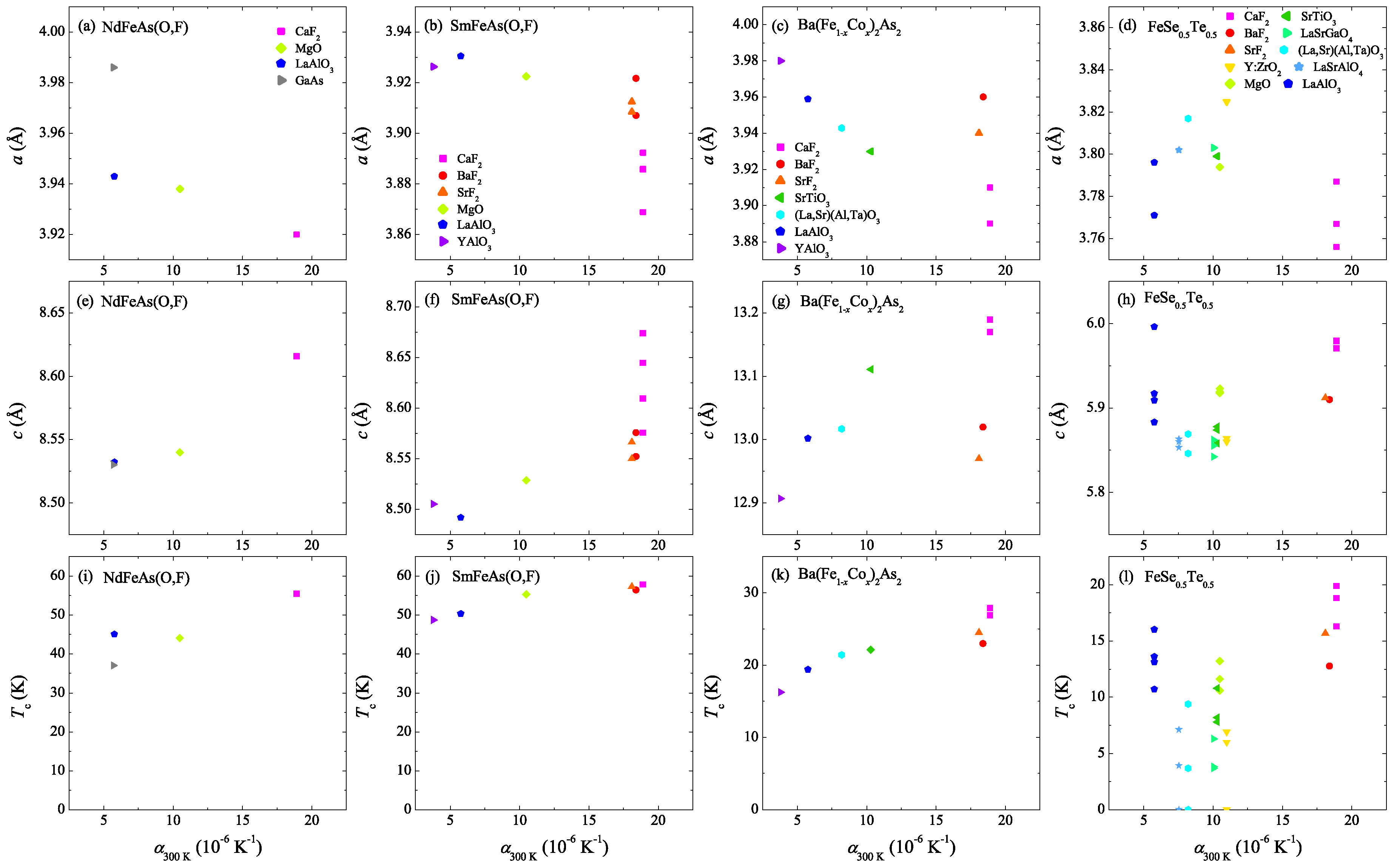
3. Substrate Materials in the Films Fabrication of Iron-Based Superconductors
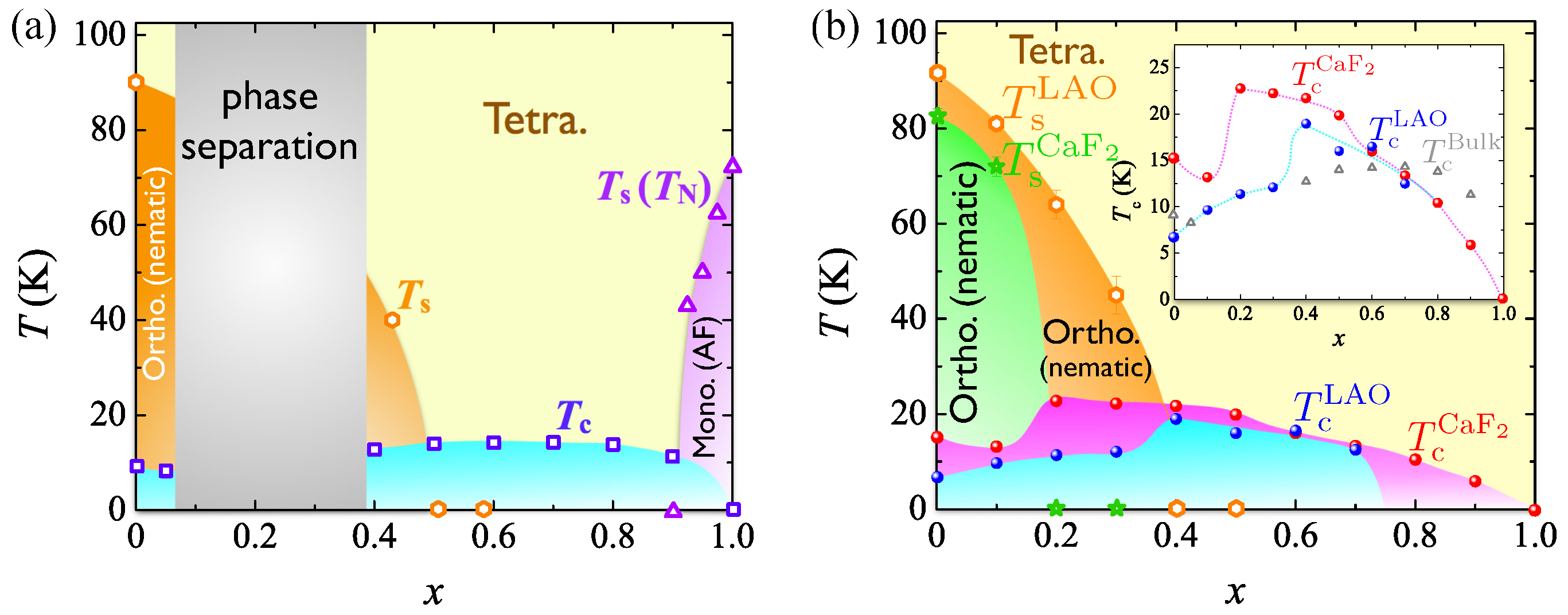
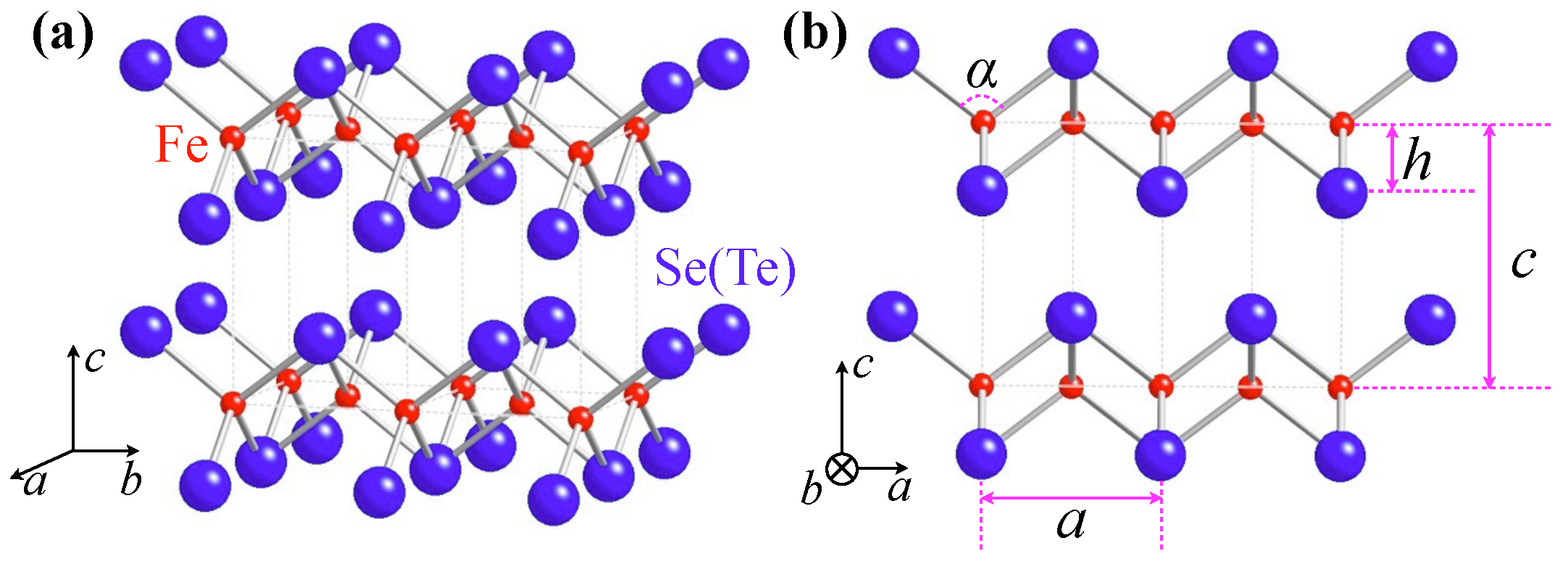
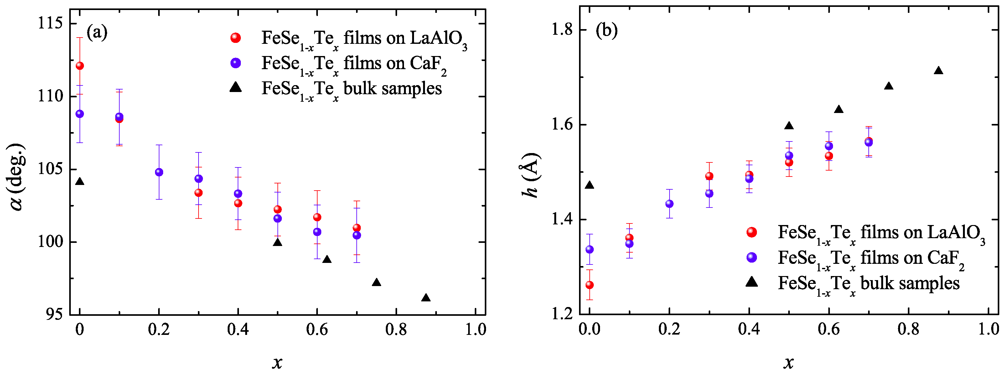
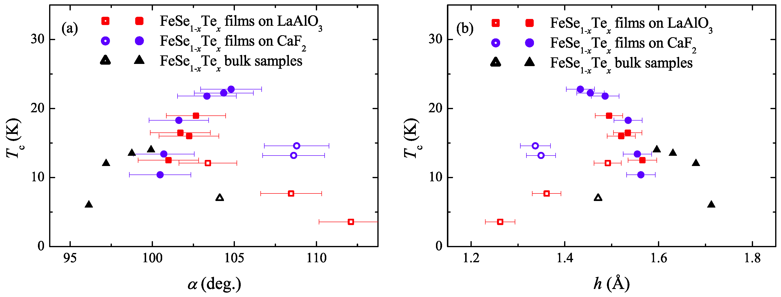
4. Comparison in Phase Diagram between Bulk Single Crystal and Epitaxial Thin Films in 11 System
5. Conclusions
Acknowledgments
Author Contributions
Conflicts of Interest
References
- Kamihara, Y.; Hiramatsu, H.; Hirano, M.; Kawamura, R.; Yanagi, H.; Kamiya, T.; Hosono, H. Iron-Based Layered Superconductor: LaOFeP. J. Am. Chem. Soc. 2006, 128, 10012. [Google Scholar] [CrossRef] [PubMed]
- Kamihara, Y.; Watanabe, T.; Hirano, M.; Hosono, H. Iron-Based Layered Superconductor La(O1−xFx)FeAs (x = 0.05–0.12) with Tc = 26 K. J. Am. Chem. Soc. 2008, 130, 3296. [Google Scholar] [CrossRef] [PubMed]
- Ren, Z.A.; Lu, W.; Yang, J.; Yi, W.; Shen, X.L.; Li, Z.C.; Che, G.C.; Dong, X.L.; Sun, L.L.; Zhou, F.; et al. Superconductivity at 55 K in Iron-Based F-Doped Layered Quaternary Compound Sm[O1−xFx]FeAs. Chin. Phys. Lett. 2008, 25, 2215. [Google Scholar]
- Hosono, H.; Kuroki, K. Iron-based superconductors: Current status of materials and pairing mechanism. Physica C 2015, 514, 399–422. [Google Scholar] [CrossRef]
- Singh, D.J.; Du, M.H. Density Functional Study of LaFeAsO1−xFx: A Low Carrier Density Superconductor Near Itinerant Magnetism. Phys. Rev. Lett. 2008, 100, 237003. [Google Scholar] [CrossRef] [PubMed]
- Subedi, A.; Zhang, L.; Singh, D.J.; Du, M.H. Density functional study of FeS, FeSe, and FeTe: Electronic structure, magnetism, phonons, and superconductivity. Phys. Rev. B 2008, 78, 134514. [Google Scholar] [CrossRef]
- Ishibashi, S.; Terakura, K.; Hosono, H. A Possible Ground State and Its Electronic Structure of a Mother Material (LaOFeAs) of New Superconductors. J. Phys. Soc. Jpn. 2008, 77, 053709. [Google Scholar] [CrossRef]
- Mazin, I.I.; Singh, D.J.; Johannes, M.D.; Du, M.H. Unconventional Superconductivity with a Sign Reversal in the Order Parameter of LaFeAsO1−xFx. Phys. Rev. Lett. 2008, 101, 057003. [Google Scholar] [CrossRef] [PubMed]
- Kuroki, K.; Onari, S.; Arita, R.; Usui, H.; Tanaka, Y.; Kontani, H.; Aoki, H. Unconventional Pairing Originating from the Disconnected Fermi Surfaces of Superconducting LaFeAsO1−xFx. Phys. Rev. Lett. 2008, 101, 087004. [Google Scholar] [CrossRef] [PubMed]
- Yanagi, Y.; Yamakawa, Y.; Ono, Y. Two types of s-wave pairing due to magnetic and orbital fluctuations in the two-dimensional 16-band d-p model for iron-based superconductors. Phys. Rev. B 2010, 81, 054518. [Google Scholar] [CrossRef]
- Kontani, H.; Onari, S. Orbital-Fluctuation-Mediated Superconductivity in Iron Pnictides: Analysis of the Five-Orbital Hubbard-Holstein Model. Phys. Rev. Lett. 2010, 104, 157001. [Google Scholar] [CrossRef] [PubMed]
- Yanagi, Y.; Yamakawa, Y.; Adachi, N.; Ono, Y. Orbital Order, Structural Transition, and Superconductivity in Iron Pnictides. J. Phys. Soc. Jpn. 2010, 79, 123707. [Google Scholar] [CrossRef]
- Liu, D.; Zhang, W.; Mou, D.; He, J.; Ou, Y.B.; Wang, Q.Y.; Li, Z.; Wang, L.; Zhao, L.; He, S.; et al. Electronic origin of high-temperature superconductivity in single-layer FeSe superconductor. Nat. Commun. 2012, 3, 931. [Google Scholar] [CrossRef] [PubMed]
- Zhang, Y.; Yang, L.X.; Xu, M.; Ye, Z.R.; Chen, F.; He, C.; Xu, H.C.; Jiang, J.; Xie, B.P.; Ying, J.J.; et al. Nodeless superconducting gap in AxFe2Se2 (A = K, Cs) revealed by angle-resolved photoemission spectroscopy. Nat. Mater. 2011, 10, 273. [Google Scholar] [CrossRef] [PubMed]
- Qian, T.; Wang, X.P.; Jin, W.C.; Zhang, P.; Richard, P.; Xu, G.; Dai, X.; Fang, Z.; Guo, J.G.; Chen, X.L.; et al. Absence of a Holelike Fermi Surface for the Iron-Based K0.8Fe1.7Se2 Superconductor Revealed by Angle-Resolved Photoemission Spectroscopy. Phys. Rev. Lett. 2011, 106, 187001. [Google Scholar] [CrossRef] [PubMed]
- Kirtley, J.R.; Tsuei, C.C.; Sun, J.Z.; Chi, C.C.; Yu-Jahnes, L.S.; Gupta, A.; Rupp, M.; Ketchen, M.B. Symmetry of the order parameter in the high-Tc superconductor YBa2Cu3O7−δ. Nature 1995, 373, 225. [Google Scholar] [CrossRef]
- Tsuei, C.C.; Kirtley, J.R. Pairing symmetry in cuprate superconductors. Rev. Mod. Phys. 2000, 72, 969–1016. [Google Scholar] [CrossRef]
- Hsu, F.C.; Luo, J.Y.; Yeh, K.W.; Chen, T.K.; Huang, T.W.; Wu, P.M.; Lee, Y.C.; Huang, Y.L.; Chu, Y.Y.; Yan, D.C.; et al. Superconductivity in the PbO-type structure α-FeSe. Proc. Natl. Acad. Sci. USA 2008, 105, 14262. [Google Scholar] [CrossRef] [PubMed]
- Putti, M.; Pallecchi, I.; Bellingeri, E.; Cimberle, M.R.; Tropeano, M.; Ferdeghini, C.; Palenzona, A.; Tarantini, C.; Yamamoto, A.; Jiang, J.; et al. New Fe-based superconductors: Properties relevant for applications. Supercond. Sci. Technol. 2010, 23, 034003. [Google Scholar] [CrossRef]
- Li, Q.; Si, W.; Dimitrov, I.K. Films of iron chalcogenide superconductors. Rep. Prog. Phys. 2011, 74, 124510. [Google Scholar] [CrossRef]
- Hiramatsu, H.; Katase, T.; Kamiya, T.; Hosono, H. Thin Film Growth and Device Fabrication of Iron-Based Superconductors. J. Phys. Soc. Jpn. 2012, 81, 011011. [Google Scholar] [CrossRef]
- Tanabe, K.; Hosono, H. Frontiers of Research on Iron-Based Superconductors toward Their Application. Jpn. J. Appl. Phys. 2012, 51, 010005. [Google Scholar] [CrossRef]
- Mele, P. Superconducting properties of iron chalcogenide thin films. Sci. Technol. Adv. Mater. 2012, 13, 054301. [Google Scholar] [CrossRef] [PubMed]
- Haindl, S.; Kidszun, M.; Oswald, S.; Hess, C.; Büchner, B.; Kölling, S.; Wilde, L.; Thersleff, T.; Yurchenko, V.V.; Jourdan, M.; et al. Thin film growth of Fe-based superconductors: from fundamental properties to functional devices. A comparative review. Rep. Prog. Phys. 2014, 77, 046502. [Google Scholar] [CrossRef] [PubMed]
- Haindl, S.; Molatta, S.; Hiramatsu, H.; Hosono, H. Recent progress in pulsed laser deposition of iron based superconductors. J. Phys. D Appl. Phys. 2016, 49, 345301. [Google Scholar] [CrossRef]
- Haindl, S.; Kidszun, M.; Kampert, E. Iron pnictide thin films: Synthesis and physics. Phys. Status Solidi (b) 2016, 254, 1600341. [Google Scholar] [CrossRef]
- Fang, M.H.; Pham, H.M.; Qian, B.; Liu, T.J.; Vehstedt, E.K.; Liu, Y.; Spinu, L.; Mao, Z.Q. Superconductivity close to magnetic instability in Fe(Se1−xTex)0.82. Phys. Rev. B 2008, 78, 224503. [Google Scholar] [CrossRef]
- Hiramatsu, H.; Katase, T.; Kamiya, T.; Hirano, M.; Hosono, H. Heteroepitaxial growth and optoelectronic properties of layered iron oxyarsenide, LaFeAsO. Appl. Phys. Lett. 2008, 93, 162504. [Google Scholar] [CrossRef]
- De la Cruz, C.; Huang, Q.; Lynn, J.W.; Li, J.; Ratcliff, W., II; Zarestky, J.L.; Mook, H.A.; Chen, G.F.; Luo, J.L.; Wang, N.L.; et al. Magnetic order close to superconductivity in the iron-based layered LaO1−xFxFeAs systems. Nature 2008, 453, 899. [Google Scholar] [CrossRef] [PubMed]
- Hiramatsu, H.; Katase, T.; Kamiya, T.; Hirano, M.; Hosono, H. Superconductivity in Epitaxial Thin Films of Co-Doped SrFe2As2 with Bilayered FeAs Structures and their Magnetic Anisotropy. Appl. Phys. Expr. 2008, 1, 101702. [Google Scholar] [CrossRef]
- Haindl, S.; Hanzawa, K.; Sato, H.; Hiramatsu, H.; Hosono, H. In-situ growth of superconducting SmO1−xFxFeAs thin films by pulsed laser deposition. Sci. Rep. 2016, 6, 35797. [Google Scholar] [CrossRef] [PubMed]
- Backen, E.; Haindl, S.; Niemeier, T.; Hühne, R.; Freudenberg, T.; Werner, J.; Behr, G.; Schultz, L.; Holzapfel, B. Growth and anisotropy of La(O, F)FeAs thin films deposited by pulsed laser deposition. Supercond. Sci. Technol. 2008, 21, 122001. [Google Scholar] [CrossRef]
- Haindl, S.; Kidszun, M.; Kauffmann, A.; Nenkov, K.; Kozlova, N.; Freudenberger, J.; Thersleff, T.; Hänisch, J.; Werner, J.; Reich, E.; et al. High Upper Critical Fields and Evidence of Weak-Link Behavior in Superconducting LaFeAsO1−xFx Thin Films. Phys. Rev. Lett. 2010, 104, 077001. [Google Scholar] [CrossRef] [PubMed]
- Kidszun, M.; Haindl, S.; Reich, E.; Hänisch, J.; Iida, K.; Schultz, L.; Holzapfel, B. Epitaxial LaFeAsO1−xFx thin films grown by pulsed laser deposition. Supercond. Sci. Technol. 2010, 23, 022002. [Google Scholar] [CrossRef]
- Kawaguchi, T.; Uemura, H.; Ohno, T.; Watanabe, R.; Tabuchi, M.; Ujihara, T.; Takenaka, K.; Takeda, Y.; Ikuta, H. Epitaxial Growth of NdFeAsO Thin Films by Molecular Beam Epitaxy. Appl. Phys. Expr. 2009, 2, 093002. [Google Scholar] [CrossRef]
- Kawaguchi, T.; Uemura, H.; Ohno, T.; Tabuchi, M.; Ujihara, T.; Takenaka, K.; Takeda, Y.; Ikuta, H. In situ growth of superconducting NdFeAs(O,F) thin films by molecular beam epitaxy. Appl. Phys. Lett. 2010, 97, 042509. [Google Scholar] [CrossRef]
- Kawaguchi, T.; Uemura, H.; Ohno, T.; Tabuchi, M.; Ujihara, T.; Takeda, Y.; Ikuta, H. Molecular Beam Epitaxy Growth of Superconducting NdFeAs(O,F) Thin Films Using a F-Getter and a Novel F-Doping Method. Appl. Phys. Expr. 2011, 4, 083102. [Google Scholar] [CrossRef]
- Ueda, S.; Takeda, S.; Takano, S.; Yamamoto, A.; Naito, M. High-Tc and high-Jc SmFeAs(O,F) films on fluoride substrates grown by molecular beam epitaxy. Appl. Phys. Lett. 2011, 99, 232505. [Google Scholar] [CrossRef]
- Kamihara, Y.; Nomura, T.; Hirano, M.; Kim, J.E.; Kato, K.; Takata, M.; Kobayashi, Y.; Kitao, S.; Higashitaniguchi, S.; Yoda, Y.; et al. Electronic and magnetic phase diagram of superconductors, SmFeAsO1−xFx. New J. Phys. 2010, 12, 033005. [Google Scholar] [CrossRef]
- Tsukada, I.; Hanawa, M.; Akiike, T.; Nabeshima, F.; Imai, Y.; Ichinose, A.; Komiya, S.; Hikage, T.; Kawaguchi, T.; Ikuta, H.; et al. Epitaxial Growth of FeSe0.5Te0.5 Thin Films on CaF2 Substrates with High Critical Current Density. Appl. Phys. Expr. 2011, 4, 053101. [Google Scholar] [CrossRef]
- Ueda, S.; Takeda, S.; Takano, S.; Naito, M. As-Grown Superconducting SmFeAs(O,F) Thin Films by Molecular Beam Epitaxy. Appl. Phys. Expr. 2012, 5, 053101. [Google Scholar] [CrossRef]
- Sugawara, H.; Tsuneki, T.; Watanabe, D.; Yamamoto, A.; Sakoda, M.; Naito, M. One-step growth of SmFeAs(O,F) films by molecular beam epitaxy using FeF2 as a fluorine source. Supercond. Sci. Technol. 2015, 28, 015005. [Google Scholar] [CrossRef]
- Chihara, M.; Sumiya, N.; Arai, K.; Ichinose, A.; Tsukada, I.; Hatano, T.; Iida, K.; Ikuta, H. Direct growth of superconducting NdFeAs(O,F) thin films by MBE. Physica C 2015, 518, 69. [Google Scholar] [CrossRef]
- Iida, K.; Kurth, F.; Chihara, M.; Sumiya, N.; Grinenko, V.; Ichinose, A.; Tsukada, I.; Hänisch, J.; Matias, V.; Hatano, T.; et al. Highly textured oxypnictide superconducting thin films on metal substrates. Appl. Phys. Lett. 2014, 105, 172602. [Google Scholar] [CrossRef]
- Ichinose, A.; Nabeshima, F.; Tsukada, I.; Hanawa, M.; Komiya, S.; Akiike, T.; Imai, Y.; Maeda, A. Microscopic analysis of the chemical reaction between Fe(Te,Se) thin films and underlying CaF2. Supercond. Sci. Technol. 2013, 26, 075002. [Google Scholar] [CrossRef][Green Version]
- Ichinose, A.; Tsukada, I.; Nabeshima, F.; Imai, Y.; Maeda, A.; Kurth, F.; Holzapfel, B.; Iida, K.; Ueda, S.; Naito, M. Induced lattice strain in epitaxial Fe-based superconducting films on CaF2 substrates: A comparative study of the microstructures of SmFeAs(O,F), Ba(Fe,Co)2As2, and FeTe0.5Se0.5. Appl. Phys. Lett. 2014, 104, 122603. [Google Scholar] [CrossRef]
- Choi, E.M.; Jung, S.G.; Lee, N.H.; Kwon, Y.S.; Kang, W.N.; Kim, D.H.; Jung, M.H.; Lee, S.I.; Sun, L. In situ fabrication of cobalt-doped SrFe2As2 thin films by using pulsed laser deposition with excimer laser. Appl. Phys. Lett. 2009, 95, 062507. [Google Scholar] [CrossRef]
- Hiramatsu, H.; Katase, T.; Kamiya, T.; Hirano, M.; Hosono, H. Water-induced superconductivity in SrFe2As2. Phys. Rev. B 2009, 80, 052501. [Google Scholar] [CrossRef]
- Katase, T.; Hiramatsu, H.; Yanagi, H.; Kamiya, T.; Hirano, M.; Hosono, H. Atomically-flat, chemically-stable, superconducting epitaxial thin film of iron-based superconductor, cobalt-doped. Solid State Commun. 2009, 149, 2121–2124. [Google Scholar] [CrossRef][Green Version]
- Lee, S.; Jiang, J.; Weiss, J.D.; Folkman, C.M.; Bark, C.W.; Tarantini, C.; Xu, A.; Abraimov, D.; Polyanskii, A.; Nelson, C.T.; et al. Weak-link behavior of grain boundaries in superconducting Ba(Fe1−xCox)2As2 bicrystals. Appl. Phys. Lett. 2009, 95, 212505. [Google Scholar] [CrossRef]
- Iida, K.; Hänisch, J.; Hühne, R.; Kurth, F.; Kidszun, M.; Haindl, S.; Werner, J.; Schultz, L.; Holzapfel, B. Strong Tc dependence for strained epitaxial Ba(Fe1−xCox)2As2 thin films. Appl. Phys. Lett. 2009, 95, 192501. [Google Scholar] [CrossRef]
- Imai, Y.; Akiike, T.; Hanawa, M.; Tsukada, I.; Ichinose, A.; Maeda, A.; Hikage, T.; Kawaguchi, T.; Ikuta, H. Systematic Comparison of Eight Substrates in the Growth of FeSe0.5Te0.5 Superconducting Thin Films. Appl. Phys. Express 2010, 3, 043102. [Google Scholar] [CrossRef]
- Lee, S.; Jiang, J.; Zhang, Y.; Bark, C.W.; Weiss, J.D.; Tarantini, C.; Nelson, C.T.; Jang, H.W.; Folkman, C.M.; Baek, S.H.; et al. Template engineering of Co-doped BaFe2As2 single-crystal thin films. Nat. Mater. 2010, 9, 397. [Google Scholar] [CrossRef] [PubMed]
- Iida, K.; Haindl, S.; Thersleff, T.; Hänisch, J.; Kurth, F.; Kidszun, M.; Hühne, R.; Mönch, I.; Schultz, L.; Holzapfel, B.; et al. Influence of Fe buffer thickness on the crystalline quality and the transport properties of Fe/Ba(Fe1−xCox)2As2 bilayers. Appl. Phys. Lett. 2010, 97, 172507. [Google Scholar] [CrossRef]
- Thersleff, T.; Iida, K.; Haindl, S.; Kidszun, M.; Pohl, D.; Hartmann, A.; Kurth, F.; Hänisch, J.; Hühne, R.; Rellinghaus, B.; et al. Coherent interfacial bonding on the FeAs tetrahedron in Fe/Ba(Fe1−xCox)2As2 bilayers. Appl. Phys. Lett. 2010, 97, 022506. [Google Scholar] [CrossRef]
- Iida, K.; Hänisch, J.; Trommler, S.; Haindl, S.; Kurth, F.; Hühne, R.; Schultz, L.; Holzapfel, B. Thickness dependence of structural and transport properties of Co-doped BaFe2As2 on Fe buffered MgO substrates. Supercond. Sci. Technol. 2011, 24, 125009. [Google Scholar] [CrossRef]
- Iida, K.; Hänisch, J.; Thersleff, T.; Kurth, F.; Kidszun, M.; Haindl, S.; Hühne, R.; Schultz, L.; Holzapfel, B. Scaling behavior of the critical current in clean epitaxial Ba(Fe1−xCox)2As2 thin films. Phys. Rev. B 2010, 81, 100507. [Google Scholar] [CrossRef]
- Katase, T.; Ishimaru, Y.; Tsukamoto, A.; Hiramatsu, H.; Kamiya, T.; Tanabe, K.; Hosono, H. Josephson junction in cobalt-doped BaFe2As2 epitaxial thin films on (La,Sr)(Al,Ta)O3 bicrystal substrates. Appl. Phys. Lett. 2010, 96, 142507. [Google Scholar] [CrossRef]
- Katase, T.; Ishimaru, Y.; Tsukamoto, A.; Hiramatsu, H.; Kamiya, T.; Tanabe, K.; Hosono, H. DC superconducting quantum interference devices fabricated using bicrystal grain boundary junctions in Co-doped BaFe2As2 epitaxial films. Supercond. Sci. Technol. 2010, 23, 082001. [Google Scholar] [CrossRef]
- Schmidt, S.; Döring, S.; Schmidl, F.; Grosse, V.; Seidel, P.; Iida, K.; Kurth, F.; Haindl, S.; Mönch, I.; Holzapfel, B. BaFe1.8Co0.2As2 thin film hybrid Josephson junctions. Appl. Phys. Lett. 2010, 97, 172504. [Google Scholar] [CrossRef][Green Version]
- Sefat, A.S.; Jin, R.; McGuire, M.A.; Sales, B.C.; Singh, D.J.; Mandrus, D. Superconductivity at 22 K in Co-Doped BaFe2As2 Crystals. Phys. Rev. Lett. 2008, 101, 117004. [Google Scholar] [CrossRef] [PubMed]
- Ishida, S.; Nakajima, M.; Liang, T.; Kihou, K.; Lee, C.H.; Iyo, A.; Eisaki, H.; Kakeshita, T.; Tomioka, Y.; Ito, T.; et al. Effect of Doping on the Magnetostructural Ordered Phase of Iron Arsenides: A Comparative Study of the Resistivity Anisotropy in Doped BaFe2As2 with Doping into Three Different Sites. J. Am. Chem. Soc. 2013, 135, 3158–3163. [Google Scholar] [CrossRef] [PubMed]
- Kurth, F.; Reich, E.; Hänisch, J.; Ichinose, A.; Tsukada, I.; Hühne, R.; Trommler, S.; Engelmann, J.; Schultz, L.; Holzapfel, B.; et al. Versatile fluoride substrates for Fe-based superconducting thin films. Appl. Phys. Lett. 2013, 102, 142601. [Google Scholar] [CrossRef]
- Rotter, M.; Tegel, M.; Johrendt, D. Superconductivity at 38 K in the Iron Arsenide (Ba1−xKx)Fe2As2. Phys. Rev. Lett. 2008, 101, 107006. [Google Scholar] [CrossRef] [PubMed]
- Takeda, S.; Ueda, S.; Yamagishi, T.; Agatsuma, S.; Takano, S.; Mitsuda, A.; Naito, M. Molecular Beam Epitaxy Growth of Superconducting Sr1−xKxFe2As2 and Ba1−xKxFe2As2. Appl. Phys. Express 2010, 3, 093101. [Google Scholar] [CrossRef]
- Agatsuma, S.; Yamagishi, T.; Takeda, S.; Naito, M. MBE growth of FeSe and Sr1−xKxFe2As2. Physica C 2010, 470, 1468. [Google Scholar] [CrossRef]
- Yamagishi, T.; Ueda, S.; Takeda, S.; Takano, S.; Mitsuda, A.; Naito, M. A study of the doping dependence of Tc in Ba1−xKxFe2As2 and Sr1−xKxFe2As2 films grown by molecular beam epitaxy. Physica C 2011, 471, 1177–1180. [Google Scholar] [CrossRef]
- Lee, N.H.; Jung, S.G.; Kim, D.H.; Kang, W.N. Potassium-doped BaFe2As2 superconducting thin films with a transition temperature of 40 K. Appl. Phys. Lett. 2010, 96, 202505. [Google Scholar] [CrossRef]
- Yuan, H.Q.; Singleton, J.; Balakirev, F.F.; Baily, S.A.; Chen, G.F.; Luo, J.L.; Wang, N.L. Nearly isotropic superconductivity in (Ba,K)Fe2As2. Nature 2009, 457, 565. [Google Scholar] [CrossRef] [PubMed]
- Yamamoto, A.; Jaroszynski, J.; Tarantini, C.; Balicas, L.; Jiang, J.; Gurevich, A.; Larbalestier, D.C.; Jin, R.; Sefat, A.S.; McGuire, M.A.; et al. Small anisotropy, weak thermal fluctuations, and high field superconductivity in Co-doped iron pnictide Ba(Fe1−xCox)2As2. Appl. Phys. Lett. 2009, 94, 062511. [Google Scholar] [CrossRef]
- Vinod, K.; Satya, A.T.; Sharma, S.; Sundar, C.S.; Bharathi, A. Upper critical field anisotropy in BaFe2−xCoxAs2 single crystals synthesized without flux. Phys. Rev. B 2011, 84, 012502. [Google Scholar] [CrossRef]
- Jiang, S.; Xing, H.; Xuan, G.; Wang, C.; Ren, Z.; Feng, C.; Dai, J.; Xu, Z.; Cao, G. Superconductivity up to 30 K in the vicinity of the quantum critical point in BaFe2(As1−xPx)2. J. Phys. Condens. Matter. 2009, 21, 382203. [Google Scholar] [CrossRef] [PubMed]
- Adachi, S.; Shimode, T.; Miura, M.; Chikumoto, N.; Takemori, A.; Nakao, K.; Oshikubo, Y.; Tanabe, K. Pulsed laser deposition of BaFe2(As,P)2 superconducting thin films with high critical current density. Supercond. Sci. Technol. 2012, 25, 105015. [Google Scholar] [CrossRef]
- Miura, M.; Maiorov, B.; Kato, T.; Shimode, T.; Wada, K.; Adachi, S.; Tanabe, K. Strongly enhanced flux pinning in one-step deposition of BaFe2(As0.66P0.33)2 superconductor films with uniformly dispersed BaZrO3 nanoparticles. Nat. Commun. 2013, 4, 2499. [Google Scholar] [CrossRef] [PubMed]
- Sakagami, A.; Kawaguchi, T.; Tabuchi, M.; Ujihara, T.; Takeda, Y.; Ikuta, H. Critical current density and grain boundary property of BaFe2(As,P)2 thin films. Physica C 2013, 494, 181–184. [Google Scholar] [CrossRef]
- Sato, H.; Hiramatsu, H.; Kamiya, T.; Hosono, H. High critical-current density with less anisotropy in BaFe2(As,P)2 epitaxial thin films: Effect of intentionally grown c-axis vortex-pinning centers. Appl. Phys. Lett. 2014, 104, 182603. [Google Scholar] [CrossRef]
- Hilgenkamp, H.; Mannhart, J. Grain boundaries in high-Tc superconductors. Rev. Mod. Phys. 2002, 74, 485–549. [Google Scholar] [CrossRef]
- Katase, T.; Ishimaru, Y.; Tsukamoto, A.; Hiramatsu, H.; Kamiya, T.; Tanabe, K.; Hosono, H. Advantageous grain boundaries in iron pnictide superconductors. Nat. Commun. 2011, 2, 409. [Google Scholar] [CrossRef] [PubMed]
- Katase, T.; Iimura, S.; Hiramatsu, H.; Kamiya, T.; Hosono, H. Identical effects of indirect and direct electron doping of superconducting BaFe2As2 thin films. Phys. Rev. B 2012, 85, 140516. [Google Scholar] [CrossRef]
- Malaeb, W.; Shimojima, T.; Ishida, Y.; Okazaki, K.; Ota, Y.; Ohgushi, K.; Kihou, K.; Saito, T.; Lee, C.H.; Ishida, S.; et al. Abrupt change in the energy gap of superconducting Ba1−xKxFe2As2 single crystals with hole doping. Phys. Rev. B 2012, 86, 165117. [Google Scholar] [CrossRef]
- Liu, C.; Kondo, T.; Fernandes, R.M.; Palczewski, A.D.; Mun, E.D.; Ni, N.; Thaler, A.N.; Bostwick, A.; Rotenberg, E.; Schmalian, J.; et al. Evidence for a Lifshitz transition in electron-doped iron arsenic superconductors at the onset of superconductivity. Nat. Phys. 2010, 6, 419–423. [Google Scholar] [CrossRef]
- Engelmann, J.; Grinenko, V.; Chekhonin, P.; Skrotzki, W.; Efremov, D.; Oswald, S.; Iida, K.; Hühne, R.; Hänisch, J.; Hoffmann, M.; et al. Strain induced superconductivity in the parent compound BaFe2As2. Nat. Commun. 2013, 4, 2877. [Google Scholar] [CrossRef] [PubMed]
- Han, Y.; Li, W.Y.; Cao, L.X.; Zhang, S.; Xu, B.; Zhao, B.R. Preparation and superconductivity of iron selenide thin films. J. Phys. Condens. Matter 2009, 21, 235702. [Google Scholar] [CrossRef] [PubMed]
- Wu, M.K.; Hsu, F.C.; Yeh, K.W.; Huang, T.W.; Luo, J.Y.; Wang, M.J.; Chang, H.H.; Chen, T.K.; Rao, S.M.; Mok, B.H.; et al. The development of the superconducting PbO-type β-FeSe and related compounds. Physica C 2009, 469, 340–349. [Google Scholar] [CrossRef]
- Nie, Y.F.; Brahimi, E.; Budnick, J.I.; Hines, W.A.; Jain, M.; Wells, B.O. Suppression of superconductivity in FeSe films under tensile strain. Appl. Phys. Lett. 2009, 94, 242505. [Google Scholar] [CrossRef]
- Kumary, T.G.; Baisnab, D.K.; Janaki, J.; Mani, A.; Satya, A.T.; Sarguna, R.M.; Ajikumar, P.K.; Tyagi, A.K.; Bharathi, A. Superconducting Fe1+δSe1−xTex thin films: growth, characterization and properties. Supercond. Sci. Technol. 2009, 22, 095018. [Google Scholar] [CrossRef]
- Bellingeri, E.; Buzio, R.; Gerbi, A.; Marrè, D.; Congiu, S.; Cimberle, M.R.; Tropeano, M.; Siri, A.S.; Palenzona, A.; Ferdeghini, C. High quality epitaxial FeSe0.5Te0.5 thin films grown on SrTiO3 substrates by pulsed laser deposition. Supercond. Sci. Technol. 2009, 22, 105007. [Google Scholar] [CrossRef]
- Si, W.; Zhou, J.; Jie, Q.; Dimitrov, I.; Solovyov, V.; Johnson, P.D.; Jaroszynski, J.; Matias, V.; Sheehan, C.; Li, Q. Iron-chalcogenide FeSe0.5Te0.5 coated superconducting tapes for high field applications. Appl. Phys. Lett. 2011, 98, 262509. [Google Scholar] [CrossRef]
- Mele, P.; Matsumoto, K.; Haruyama, Y.; Mukaida, M.; Yoshida, Y.; Kiss, T. Fabrication of Fe-Te-S Superconducting Epitaxial Thin Films by Pulsed Laser Deposition. Appl. Phys. Expr. 2009, 2, 073002. [Google Scholar] [CrossRef]
- Imai, Y.; Tanaka, R.; Akiike, T.; Hanawa, M.; Tsukada, I.; Maeda, A. Superconductivity of FeSe0.5Te0.5 Thin Films Grown by Pulsed Laser Deposition. Jpn. J. Appl. Phys. 2010, 49, 023101. [Google Scholar] [CrossRef]
- Huang, S.X.; Chien, C.L.; Thampy, V.; Broholm, C. Control of Tetrahedral Coordination and Superconductivity in FeSe0.5Te0.5 Thin Films. Phys. Rev. Lett. 2010, 104, 217002. [Google Scholar] [CrossRef] [PubMed]
- Bellingeri, E.; Pallecchi, I.; Buzio, R.; Gerbi, A.; Marré, D.; Cimberle, M.R.; Tropeano, M.; Putti, M.; Palenzona, A.; Ferdeghini, C. Tc = 21K in epitaxial FeSe0.5Te0.5 thin films with biaxial compressive strain. Appl. Phys. Lett. 2010, 96, 102512. [Google Scholar] [CrossRef]
- Nabeshima, F.; Imai, Y.; Hanawa, M.; Tsukada, I.; Maeda, A. Enhancement of the superconducting transition temperature in FeSe epitaxial thin films by anisotropic compression. Appl. Phys. Lett. 2013, 103, 172602. [Google Scholar] [CrossRef]
- Maeda, A.; Nabeshima, F.; Takahashi, H.; Okada, T.; Imai, Y.; Tsukada, I.; Hanawa, M.; Komiya, S.; Ichinose, A. Synthesis, characterization, Hall effect and THz conductivity of epitaxial thin films of Fe chalcogenide superconductors. Appl. Sur. Sci. 2014, 312, 43. [Google Scholar] [CrossRef]
- Lee, C.H.; Iyo, A.; Eisaki, H.; Kito, H.; Teresa Fernandez-Diaz, M.; Ito, T.; Kihou, K.; Matsuhata, H.; Braden, M.; Yamada, K. Effect of Structural Parameters on Superconductivity in Fluorine-Free LnFeAsO1−y (Ln = La, Nd). J. Phys. Soc. Jpn. 2008, 77, 083704. [Google Scholar] [CrossRef]
- Lee, C.H.; Kihou, K.; Iyo, A.; Kito, H.; Shirage, P.; Eisaki, H. Relationship between crystal structure and superconductivity in iron-based superconductors. Solid State Commun. 2012, 152, 644. [Google Scholar] [CrossRef]
- Tsukada, A.; Luna, K.E.; Hammond, R.H.; Beasley, M.R.; Zhao, J.F.; Risbud, S.H. Pulsed laser deposition conditions and superconductivity of FeSe thin films. Appl. Phys. A 2011, 104, 311–318. [Google Scholar] [CrossRef][Green Version]
- Wang, Q.Y.; Li, Z.; Zhang, W.H.; Zhang, Z.C.; Zhang, J.S.; Li, W.; Ding, H.; Ou, Y.B.; Deng, P.; Chang, K.; et al. Interface-Induced High-Temperature Superconductivity in Single Unit-Cell FeSe Films on SrTiO3. Chin. Phys. Lett. 2012, 29, 37402. [Google Scholar] [CrossRef]
- Bellingeri, E.; Kawale, S.; Braccini, V.; Buzio, R.; Gerbi, A.; Martinelli, A.; Putti, M.; Pallecchi, I.; Balestrino, G.; Tebano, A.; et al. Tuning of the superconducting properties of FeSe0.5Te0.5 thin films through the substrate effect. Supercond. Sci. Technol. 2012, 25, 084022. [Google Scholar] [CrossRef]
- Hanawa, M.; Ichinose, A.; Komiya, S.; Tsukada, I.; Imai, Y.; Maeda, A. Empirical Selection Rule of Substrate Materials for Iron Chalcogenide Superconducting Thin Films. Jpn. J. Appl. Phys. 2012, 51, 010104. [Google Scholar] [CrossRef]
- Tsukada, I.; Ichinose, A.; Nabeshima, F.; Imai, Y.; Maeda, A. Origin of lattice compression of FeSe1−xTex thin films on CaF2 substrates. AIP Adv. 2016, 6, 095314. [Google Scholar] [CrossRef]
- Iida, K.; Hänisch, J.; Schulze, M.; Aswartham, S.; Wurmehl, S.; Büchner, B.; Schultz, L.; Holzapfel, B. Generic Fe buffer layers for Fe-based superconductors: Epitaxial FeSe1−xTex thin films. Appl. Phys. Lett. 2011, 99, 202503. [Google Scholar] [CrossRef]
- Si, W.; Han, S.J.; Shi, X.; Ehrlich, S.N.; Jaroszynski, J.; Goyal, A.; Li, Q. High current superconductivity in FeSe0.5Te0.5-coated conductors at 30 tesla. Nat. Commun. 2013, 4, 1347. [Google Scholar] [CrossRef] [PubMed]
- Molatta, S.; Haindl, S.; Trommler, S.; Schulze, M.; Wurmehl, S.; Hühne, R. Interface control by homoepitaxial growth in pulsed laser deposited iron chalcogenide thin films. Sci. Rep. 2015, 5, 16334. [Google Scholar] [CrossRef] [PubMed]
- Tkachenko, O.; Morawski, A.; Zaleski, A.J.; Przyslupski, P.; Dietl, T.; Diduszko, R.; Presz, A.; Werner-Malento, K. Synthesis, Crystal Growth and Epitaxial Layers Growth of c2 a0FeSe0.88 Superconductor and Other Poison Materials byc2a0Use c2a0ofc2a0High Gas Pressure Trap System. J. Supercond. Nov. Magn. 2009, 22, 599–602. [Google Scholar] [CrossRef]
- Schneider, R.; Zaitsev, A.G.; Fuchs, D.; v. Löhneysen, H. Superconductor-Insulator Quantum Phase Transition in Disordered FeSe Thin Films. Phys. Rev. Lett. 2012, 108, 257003. [Google Scholar] [CrossRef] [PubMed]
- Speller, S.C.; Aksoy, C.; Saydam, M.; Taylor, H.; Burnell, G.; Boothroyd, A.T.; Grovenor, C.R.M. Analysis of FeySe1−xTex thin films grown by radio frequency sputtering. Supercond. Sci. Technol. 2011, 24, 075023. [Google Scholar] [CrossRef]
- Mousavi, T.; Grovenor, C.; Speller, S. Characterization of superconducting Fey(Se1−xTex) thin films deposited on MgO substrates by sputtering. J. Mater. Sci. 2015, 50, 6970–6978. [Google Scholar] [CrossRef]
- Pawar, S.; Moholkar, A.; Suryavanshi, U.; Rajpure, K.; Bhosale, C. Electrosynthesis and characterization of iron selenide thin films. Sol. Energy Mater. Sol. Cells 2007, 91, 560–565. [Google Scholar] [CrossRef]
- Thanikaikarasan, S.; Mahalingam, T.; Sundaram, K.; Kathalingam, A.; Kim, Y.D.; Kim, T. Growth and characterization of electrosynthesized iron selenide thin films. Vacuum 2009, 83, 1066–1072. [Google Scholar] [CrossRef]
- Thanikaikarasan, S.; Mahalingam, T.; Raja, M.; Kim, T.; Kim, Y.D. Characterization of electroplated FeSe thin films. J. Mater. Sci. Mater. Electron. 2009, 20, 727–734. [Google Scholar] [CrossRef]
- Chen, P.; Hu, S.; Liu, R.; Huang, C. Electrodeposition of nano-dimensioned FeSe. Thin Solid Films 2011, 519, 8397–8400. [Google Scholar] [CrossRef]
- Demura, S.; Ozaki, T.; Okazaki, H.; Mizuguchi, Y.; Kawasaki, Y.; Deguchi, K.; Watanabe, T.; Hara, H.; Yamaguchi, T.; Takeya, H.; et al. Electrochemical Synthesis of Iron-Based Superconductor FeSe Films. J. Phys. Soc. Jpn. 2012, 81, 043702. [Google Scholar] [CrossRef]
- Demura, S.; Okazaki, H.; Ozaki, T.; Hara, H.; Kawasaki, Y.; Deguchi, K.; Watanabe, T.; Denholme, S.J.; Mizuguchi, Y.; Yamaguchi, T.; et al. Electrodeposition as a new route to synthesize superconducting FeSe. Solid State Commun. 2013, 154, 40–42. [Google Scholar] [CrossRef]
- Li, L.; Yang, Z.R.; Sun, Y.P.; Zhang, J.Y.; Shen, D.Z.; Zhang, Y.H. Superconductivity and magnetism in FeSe thin films grown by metal-organic chemical vapor deposition. Supercond. Sci. Technol. 2011, 24, 015010. [Google Scholar] [CrossRef]
- Hussain, R.A.; Badshah, A.; Younis, A.; Khan, M.D.; Akhtar, J. Iron selenide films by aerosol assisted chemical vapor deposition from single source organometallic precursor in the presence of surfactants. Thin Solid Films 2014, 567, 58–63. [Google Scholar] [CrossRef]
- Eisterer, M.; Raunicher, R.; Weber, H.W.; Bellingeri, E.; Cimberle, M.R.; Pallecchi, I.; Putti, M.; Ferdeghini, C. Anisotropic critical currents in FeSe0.5Te0.5 films and the influence of neutron irradiation. Supercond. Sci. Technol. 2011, 24, 065016. [Google Scholar] [CrossRef]
- Mele, P.; Matsumoto, K.; Haruyama, Y.; Mukaida, M.; Yoshida, Y.; Ichino, Y.; Kiss, T.; Ichinose, A. In-field characterization of FeTe0.8S0.2 epitaxial thin films with enhanced superconducting properties. Supercond. Sci. Technol. 2010, 23, 052001. [Google Scholar] [CrossRef]
- Iida, K.; Hänisch, J.; Reich, E.; Kurth, F.; Hühne, R.; Schultz, L.; Holzapfel, B.; Ichinose, A.; Hanawa, M.; Tsukada, I.; et al. Intrinsic pinning and the critical current scaling of clean epitaxial Fe(Se,Te) thin films. Phys. Rev. B 2013, 87, 104510. [Google Scholar] [CrossRef]
- Braccini, V.; Kawale, S.; Reich, E.; Bellingeri, E.; Pellegrino, L.; Sala, A.; Putti, M.; Higashikawa, K.; Kiss, T.; Holzapfel, B.; et al. Highly effective and isotropic pinning in epitaxial Fe(Se,Te) thin films grown on CaF2 substrates. Appl. Phys. Lett. 2013, 103, 172601. [Google Scholar] [CrossRef]
- Ozaki, T.; Wu, L.; Zhang, C.; Jaroszynski, J.; Si, W.; Zhou, J.; Zhu, Y.; Li, Q. A route for a strong increase of critical current in nanostrained iron-based superconductors. Nat. Commun. 2016, 7, 13036. [Google Scholar] [CrossRef] [PubMed]
- Han, Y.; Li, W.Y.; Cao, L.X.; Wang, X.Y.; Xu, B.; Zhao, B.R.; Guo, Y.Q.; Yang, J.L. Superconductivity in Iron Telluride Thin Films under Tensile Stress. Phys. Rev. Lett. 2010, 104, 017003. [Google Scholar] [CrossRef] [PubMed]
- Si, W.; Jie, Q.; Wu, L.; Zhou, J.; Gu, G.; Johnson, P.D.; Li, Q. Superconductivity in epitaxial thin films of Fe1.08Te:Ox. Phys. Rev. B 2010, 81, 092506. [Google Scholar] [CrossRef]
- Nie, Y.F.; Telesca, D.; Budnick, J.I.; Sinkovic, B.; Wells, B.O. Superconductivity induced in iron telluride films by low-temperature oxygen incorporation. Phys. Rev. B 2010, 82, 020508. [Google Scholar] [CrossRef]
- Tsukada, I.; Hanawa, M.; Komiya, S.; Ichinose, A.; Akiike, T.; Imai, Y.; Maeda, A. Mobility Analysis of FeTe Thin Films. J. Phys. Soc. Jpn. 2011, 80, 023712. [Google Scholar] [CrossRef]
- Narangammana, L.K.; Liu, X.; Nie, Y.F.; Rueckert, F.J.; Budnick, J.I.; Hines, W.A.; Gu, G.; Wells, B.O. Low temperature crystal structure and large lattice discontinuity at Tc in superconducting FeTeOx films. Appl. Phys. Lett. 2013, 103, 102604. [Google Scholar] [CrossRef]
- Tsukada, I.; Hanawa, M.; Komiya, S.; Akiike, T.; Tanaka, R.; Imai, Y.; Maeda, A. Hall effect in superconducting Fe(Se0.5Te0.5) thin films. Phys. Rev. B 2010, 81, 054515. [Google Scholar] [CrossRef]
- Tsukada, I.; Nabeshima, F.; Ichinose, A.; Komiya, S.; Hanawa, M.; Imai, Y.; Maeda, A. Crossover from hole- to electron-dominant regions in iron-chalcogenide superconductors induced by Te/Se substitution. Jpn. J. Appl. Phys. 2015, 54, 043102. [Google Scholar] [CrossRef]
- Dimitrov, I.K.; Si, W.D.; Ku, W.; Han, S.J.; Jaroszynski, J. Unusual persistence of superconductivity against high magnetic fields in the strongly-correlated iron-chalcogenide film FeTe:Ox. Low Temp. Phys. 2013, 39, 680–684. [Google Scholar] [CrossRef][Green Version]
- Zhuang, J.; Yeoh, W.K.; Cui, X.; Xu, X.; Du, Y.; Shi, Z.; Ringer, S.P.; Wang, X.; Dou, S.X. Unabridged phase diagram for single-phased FeSexTe1−x thin films. Sci. Rep. 2014, 4, 7273. [Google Scholar] [CrossRef] [PubMed]
- Imai, Y.; Sawada, Y.; Nabeshima, F.; Maeda, A. Suppression of phase separation and giant enhancement of superconducting transition temperature in FeSe1−xTex thin films. Proc. Natl. Acad. Sci. USA 2015, 112, 1937–1940. [Google Scholar] [CrossRef] [PubMed]
- Imai, Y.; Sawada, Y.; Asami, D.; Nabeshima, F.; Maeda, A. Superconducting properties of FeSe1−xTex films with. Physica C 2016, 530, 24. [Google Scholar] [CrossRef]
- Imai, Y.; Sawada, Y.; Nabeshima, F.; Asami, D.; Kawai, M.; Maeda, A. Control of structural transition in FeSe1−xTex thin films by changing substrate materials. Sci. Rep. 2017, 7, 46653. [Google Scholar] [CrossRef] [PubMed]
- Noji, T.; Hatakeda, T.; Hosono, S.; Kawamata, T.; Kato, M.; Koike, Y. Synthesis and post-annealing effects of alkaline-metal-ethylenediamine-intercalated superconductors Ax(C2H8N2)yFe2−zSe2 (A = Li, Na) with Tc = 45 K. Physica C 2014, 504, 8–11. [Google Scholar] [CrossRef]
- Hosono, S.; Noji, T.; Hatakeda, T.; Kawamata, T.; Kato, M.; Koike, Y. New Superconducting Phase of Lix(C6H16N2)yFe2−zSe2 with Tc = 41 K Obtained through the Post-Annealing. J. Phys. Soc. Jpn. 2016, 85, 013702. [Google Scholar] [CrossRef]
- Nabeshima, F.; Imai, Y.; Ichinose, A.; Tsukada, I.; Maeda, A. Growth and transport properties of FeSe/FeTe superlattice thin films. Jpn. J. Appl. Phys. 2017, 56, 020308. [Google Scholar] [CrossRef]
- Lubashevsky, Y.; Lahoud, E.; Chashka, K.; Podolsky, D.; Kanigel, A. Shallow pockets and very strong coupling superconductivity in FeSexTe1−x. Nat. Phys. 2012, 8, 309–312. [Google Scholar] [CrossRef]
- Okazaki, K.; Ito, Y.; Ota, Y.; Kotani, Y.; Shimojima, T.; Kiss, T.; Watanabe, S.; Chen, C.T.; Niitaka, S.; Hanaguri, T.; et al. Superconductivity in an electron band just above the Fermi level: Possible route to BCS-BEC superconductivity. Sci. Rep. 2014, 4, 4109. [Google Scholar] [CrossRef] [PubMed]
- Kasahara, S.; Watashige, T.; Hanaguri, T.; Kohsaka, Y.; Yamashita, T.; Shimoyama, Y.; Mizukami, Y.; Endo, R.; Ikeda, H.; Aoyama, K.; et al. Field-induced superconducting phase of FeSe in the BCS-BEC cross-over. Proc. Natl. Acad. Sci. USA 2014, 111, 16309–16313. [Google Scholar] [CrossRef] [PubMed]
- Tan, S.; Zhang, Y.; Xia, M.; Ye, Z.; Chen, F.; Xie, X.; Peng, R.; Xu, D.; Fan, Q.; Xu, H.; et al. Interface-induced superconductivity and strain-dependent spin density waves in FeSe/SrTiO3 thin films. Nat. Mater. 2013, 12, 634–640. [Google Scholar] [CrossRef] [PubMed]
- He, S.; He, J.; Zhang, W.; Zhao, L.; Liu, D.; Liu, X.; Mou, D.; Ou, Y.B.; Wang, Q.Y.; Li, Z.; et al. Phase diagram and electronic indication of high-temperature superconductivity at 65 K in single-layer FeSe films. Nat. Mater. 2013, 12, 605–610. [Google Scholar] [CrossRef] [PubMed]
- Wen, H.Z.; Yi, S.; Jin, S.Z.; Fang, S.L.; Ming, H.G.; Yan, F.Z.; Hui, M.Z.; Jun, P.P.; Ying, X.; Hui, C.W.; et al. Direct Observation of High-Temperature Superconductivity in One-Unit-Cell FeSe Films. Chin. Phys. Lett. 2014, 31, 017401. [Google Scholar]
- Deng, L.Z.; Lv, B.; Wu, Z.; Xue, Y.Y.; Zhang, W.H.; Li, F.S.; Wang, L.L.; Ma, X.C.; Xue, Q.K.; Chu, C.W. Meissner and mesoscopic superconducting states in 1–4 unit-cell FeSe films. Phys. Rev. B 2014, 90, 214513. [Google Scholar] [CrossRef]
- Zhang, Z.; Wang, Y.H.; Song, Q.; Liu, C.; Peng, R.; Moler, K.; Feng, D.; Wang, Y. Onset of the Meissner effect at 65 K in FeSe thin film grown on Nb-doped SrTiO3 substrate. Sci. Bull. 2015, 60, 1301–1304. [Google Scholar] [CrossRef]
- Ge, J.F.; Liu, Z.L.; Liu, C.; Gao, C.L.; Qian, D.; Xue, Q.K.; Liu, Y.; Jia, J.F. Superconductivity above 100 K in single-layer FeSe films on doped SrTiO3. Nat. Mater. 2015, 14, 285–289. [Google Scholar] [CrossRef] [PubMed]
- Peng, R.; Shen, X.P.; Xie, X.; Xu, H.C.; Tan, S.Y.; Xia, M.; Zhang, T.; Cao, H.Y.; Gong, X.G.; Hu, J.P.; et al. Measurement of an Enhanced Superconducting Phase and a Pronounced Anisotropy of the Energy Gap of a Strained FeSe Single Layer in FeSe/Nb:SrTiO3/KTaO3 Heterostructures Using Photoemission Spectroscopy. Phys. Rev. Lett. 2014, 112, 107001. [Google Scholar] [CrossRef] [PubMed]
- Miyata, Y.; Nakayama, K.; Sugawara, K.; Sato, T.; Takahashi, T. High-temperature superconductivity in potassium-coated multilayer FeSe thin films. Nat. Mater. 2015, 14, 775–779. [Google Scholar] [CrossRef] [PubMed]
- Tang, C.; Zhang, D.; Zang, Y.; Liu, C.; Zhou, G.; Li, Z.; Zheng, C.; Hu, X.; Song, C.; Ji, S.; et al. Superconductivity dichotomy in K-coated single and double unit cell FeSe films on SrTiO3. Phys. Rev. B 2015, 92, 180507. [Google Scholar] [CrossRef]
- Wen, C.H.P.; Xu, H.C.; Chen, C.; Huang, Z.C.; Lou, X.; Pu, Y.J.; Song, Q.; Xie, B.P.; Abdel-Hafiez, M.; Chareev, D.A.; et al. Anomalous correlation effects and unique phase diagram of electron-doped FeSe revealed by photoemission spectroscopy. Nat. Commun. 2016, 7, 10840. [Google Scholar] [CrossRef] [PubMed]
- Song, C.L.; Zhang, H.M.; Zhong, Y.; Hu, X.P.; Ji, S.H.; Wang, L.; He, K.; Ma, X.C.; Xue, Q.K. Observation of Double-Dome Superconductivity in Potassium-Doped FeSe Thin Films. Phys. Rev. Lett. 2016, 116, 157001. [Google Scholar] [CrossRef] [PubMed]
- Tang, C.; Liu, C.; Zhou, G.; Li, F.; Ding, H.; Li, Z.; Zhang, D.; Li, Z.; Song, C.; Ji, S.; et al. Interface-enhanced electron-phonon coupling and high-temperature superconductivity in potassium-coated ultrathin FeSe films on SrTiO3. Phys. Rev. B 2016, 93, 020507. [Google Scholar] [CrossRef]
- Zhang, W.H.; Liu, X.; Wen, C.H.P.; Peng, R.; Tan, S.Y.; Xie, B.P.; Zhang, T.; Feng, D.L. Effects of Surface Electron Doping and Substrate on the Superconductivity of Epitaxial FeSe Films. Nano Lett. 2016, 16, 1969–1973. [Google Scholar] [CrossRef] [PubMed]
- Shiogai, J.; Ito, Y.; Mitsuhashi, T.; Nojima, T.; Tsukazaki, A. Electric-field-induced superconductivity in electrochemically etched ultrathin FeSe films on SrTiO3 and MgO. Nat. Phys. 2016, 12, 42–46. [Google Scholar] [CrossRef]
- Lei, B.; Cui, J.H.; Xiang, Z.J.; Shang, C.; Wang, N.Z.; Ye, G.J.; Luo, X.G.; Wu, T.; Sun, Z.; Chen, X.H. Evolution of High-Temperature Superconductivity from a Low-Tc Phase Tuned by Carrier Concentration in FeSe Thin Flakes. Phys. Rev. Lett. 2016, 116, 077002. [Google Scholar] [CrossRef] [PubMed]
- Hanzawa, K.; Sato, H.; Hiramatsu, H.; Kamiya, T.; Hosono, H. Electric field-induced superconducting transition of insulating FeSe thin film at 35 K. Proc. Natl. Acad. Sci. USA 2016, 113, 3986–3990. [Google Scholar] [CrossRef] [PubMed]
- Saito, Y.; Nojima, T.; Iwasa, Y. Highly crystalline 2D superconductors. Nat. Rev. Mats. 2016, 2, 16094. [Google Scholar] [CrossRef]
- Lee, D.H. What makes the Tc of FeSe/SrTiO3 so high? Chin. Phys. B 2015, 24, 117405. [Google Scholar] [CrossRef]
- Lee, J.J.; Schmitt, F.T.; Moore, R.G.; Johnston, S.; Cui, Y.T.; Li, W.; Yi, M.; Liu, Z.K.; Hashimoto, M.; Zhang, Y.; et al. Interfacial mode coupling as the origin of the enhancement of Tc in FeSe films on SrTiO3. Nature 2014, 515, 245–248. [Google Scholar] [CrossRef] [PubMed]
- Tian, Y.C.; Zhang, W.H.; Li, F.S.; Wu, Y.L.; Wu, Q.; Sun, F.; Zhou, G.Y.; Wang, L.; Ma, X.; Xue, Q.K.; et al. Ultrafast Dynamics Evidence of High Temperature Superconductivity in Single Unit Cell FeSe on SrTiO3. Phys. Rev. Lett. 2016, 116, 107001. [Google Scholar] [CrossRef] [PubMed]
- Zhang, S.; Guan, J.; Jia, X.; Liu, B.; Wang, W.; Li, F.; Wang, L.; Ma, X.; Xue, Q.; Zhang, J.; et al. Role of SrTiO3 phonon penetrating into thin FeSe films in the enhancement of superconductivity. Phys. Rev. B 2016, 94, 081116. [Google Scholar] [CrossRef]
- Peng, R.; Xu, H.C.; Tan, S.Y.; Cao, H.Y.; Xia, M.; Shen, X.P.; Huang, Z.C.; Wen, C.; Song, Q.; Zhang, T.; et al. Tuning the band structure and superconductivity in single-layer FeSe by interface engineering. Nat. Commun. 2014, 5, 5044. [Google Scholar] [CrossRef] [PubMed]
- Li, F.; Ding, H.; Tang, C.; Peng, J.; Zhang, Q.; Zhang, W.; Zhou, G.; Zhang, D.; Song, C.L.; He, K.; et al. Interface-enhanced high-temperature superconductivity in single-unit-cell FeTe1−xSex films on SrTiO3. Phys. Rev. B 2015, 91, 220503. [Google Scholar] [CrossRef]
- Zhou, G.; Zhang, D.; Liu, C.; Tang, C.; Wang, X.; Li, Z.; Song, C.; Ji, S.; He, K.; Wang, L.; Ma, X.; Xue, Q.K. Interface induced high temperature superconductivity in single unit-cell FeSe on SrTiO3(110). Appl. Phys. Lett. 2016, 108, 202603. [Google Scholar] [CrossRef]
- Zhang, P.; Peng, X.L.; Qian, T.; Richard, P.; Shi, X.; Ma, J.Z.; Fu, B.B.; Guo, Y.L.; Han, Z.Q.; Wang, S.C.; et al. Observation of high-Tc superconductivity in rectangular FeSe/SrTiO3(110) monolayers. Phys. Rev. B 2016, 94, 104510. [Google Scholar] [CrossRef]
- Ding, H.; Lv, Y.F.; Zhao, K.; Wang, W.L.; Wang, L.; Song, C.L.; Chen, X.; Ma, X.C.; Xue, Q.K. High-Temperature Superconductivity in Single-Unit-Cell FeSe Films on Anatase TiO2(001). Phys. Rev. Lett. 2016, 117, 067001. [Google Scholar] [CrossRef] [PubMed]
- Rebec, S.N.; Jia, T.; Zhang, C.; Hashimoto, M.; Lu, D.H.; Moore, R.G.; Shen, Z.X. Coexistence of Replica Bands and Superconductivity in FeSe Monolayer Films. Phys. Rev. Lett. 2017, 118, 067002. [Google Scholar] [CrossRef] [PubMed]
- Ginzburg, V. On surface superconductivity. Phys. Lett. 1964, 13, 101–102. [Google Scholar] [CrossRef]
- Fang, L.; Cheng, P.; Jia, Y.; Zhu, X.; Luo, H.; Mu, G.; Gu, C.; Wen, H.H. Growth of single crystals at ambient pressure and their transport properties. J. Cryst. Growth 2009, 311, 358–361. [Google Scholar] [CrossRef]
- Karpinski, J.; Zhigadlo, N.; Katrych, S.; Bukowski, Z.; Moll, P.; Weyeneth, S.; Keller, H.; Puzniak, R.; Tortello, M.; Daghero, D.; et al. Single crystals of LnFeAsO1−xFx (Ln = La, Pr, Nd, Sm, Gd) and Ba1−xRbxFe2As2: Growth, structure and superconducting properties. Physica C 2009, 469, 370–380. [Google Scholar] [CrossRef]
- Itoh, T.; Mori, M.; Inukai, M.; Nitani, H.; Yamamoto, T.; Miyanaga, T.; Igawa, N.; Kitamura, N.; Ishida, N.; Idemoto, Y. Effect of Annealing on Crystal and Local Structures of Doped Zirconia Using Experimental and Computational Methods. J. Phys. Chem. C 2015, 119, 8447–8458. [Google Scholar] [CrossRef]
- Cao, X.Q.; Vassen, R.; Jungen, W.; Schwartz, S.; Tietz, F.; Stöver, D. Thermal Stability of Lanthanum Zirconate Plasma-Sprayed Coating. J. Am. Ceram. Soc. 2001, 84, 2086. [Google Scholar] [CrossRef]
- Diehl, R.; Brandt, G. Crystal structure refinement of YAlO3, a promising laser material. Mater. Res. Bull. 1975, 10, 85–90. [Google Scholar] [CrossRef]
- Chaix-Pluchery, O.; Chenevier, B.; Robles, J.J. Anisotropy of thermal expansion in YAlO3 and NdGaO3. Appl. Phys. Lett. 2005, 86, 251911. [Google Scholar] [CrossRef]
- Magrez, A.; Morniroli, J.; Caldes, M.; Marie, A.; Joubert, O.; Brohan, L. Using CBED and crystallographic image processing to evidence a structural distortion in a new family of ionic conductor Sr1−xLa1+xAl1−xMgxO4 (0 ≤ x ≤ 0.7). J. Solid State Chem. 2003, 172, 243–251. [Google Scholar] [CrossRef]
- Byszewski, P.; Domagała, J.; Fink-Finowicki, J.; Pajaczkowska, A. Thermal properties of CaNdAlO4 and SrLaAlO4 single crystals. Mater. Res. Bull. 1992, 27, 483–490. [Google Scholar] [CrossRef]
- Lehnert, H.; Boysen, H.; Schneider, J.; Frey, F.; Hohlwein, D.; Radaelli, P.; Ehrenberg, H. A powder diffraction study of the phase transition in LaAlO3. Z. Kristallogr. 2000, 215, 536–541. [Google Scholar] [CrossRef]
- Chakoumakos, B.C.; Schlom, D.G.; Urbanik, M.; Luine, J. Thermal expansion of LaAlO3 and (La,Sr)(Al,Ta)O3 substrate materials for superconducting thin-film device applications. J. Appl. Phys. 1998, 83, 1979–1982. [Google Scholar] [CrossRef]
- Britten, J.F.; Dabkowska, H.A.; Dabkowski, A.B.; Greedan, J.E.; Campbell, J.L.; Teesdale, W.J. Czochralski-Grown SrLaGaO4. Acta Crystallogr. C 1995, 51, 1975–1977. [Google Scholar] [CrossRef]
- Hontsu, S.; Ishii, J.; Kawai, T.; Kawai, S. LaSrGaO4 substrate gives oriented crystalline YBa2Cu3O7−y films. Appl. Phys. Lett. 1991, 59, 2886–2888. [Google Scholar] [CrossRef]
- Mateika, D.; Kohler, H.; Laudan, H.; Völkel, E. Mixed-perovskite substrates for high-Tc superconductors. J. Cryst. Growth 1991, 109, 441–446. [Google Scholar] [CrossRef]
- Nelmes, R.J.; Meyer, G.M.; Hutton, J. Thermal motion in SrTiO3 at room temperature: Anharmonic or disordered? Ferroelectrics 1978, 21, 461–462. [Google Scholar] [CrossRef]
- Touloukian, Y.; Kirby, R.; Taylor, E.; Lee, T. Thermophysical Properties of Matter-The TPRC Data Series. Volume 13. Thermal Expansion-Nonmetallic Solids; Defense Technical Information Center: Fort Belvoir, VA, USA, 1977. [Google Scholar]
- Hazen, R.M. Effects of temperature and pressure on the cell dimension and X-ray temperature factors of periclas. Am. Mineral. 1976, 61, 266–271. [Google Scholar]
- Cheetham, A.K.; Fender, B.E.F.; Cooper, M.J. Defect structure of calcium fluoride containing excess anions I. Bragg scattering. J. Phys. C Solid State Phys. 1971, 4, 3107. [Google Scholar] [CrossRef]
- Roberts, R.B.; White, G.K. Thermal expansion of fluorites at high temperatures. J. Phys. C Solid State Phys. 1986, 19, 7167. [Google Scholar] [CrossRef]
- Forsyth, J.B.; Wilson, C.C.; Sabine, T.M. A time-of-flight neutron diffraction study of anharmonic thermal vibrations in SrF2, at the spallation neutron source ISIS. Acta Crystallogr. A 1989, 45, 244–247. [Google Scholar] [CrossRef]
- Radtke, S.; Brown, G.E. Frankdicksonite, BaF2, a new mineral from Nevada. Am. Mineral. 1974, 59, 885–888. [Google Scholar]
- Stevenson, A.W. Thermal vibrations and bonding in GaAs: An extended-face crystal study. Acta Crystallogr. A 1994, 50, 621–632. [Google Scholar] [CrossRef]
- Uemura, H.; Kawaguchi, T.; Ohno, T.; Tabuchi, M.; Ujihara, T.; Takeda, Y.; Ikuta, H. Substrate dependence of the superconducting properties of NdFeAs(O,F) thin films. Solid State Commun. 2012, 152, 735–739. [Google Scholar] [CrossRef]
- Takano, S.; Ueda, S.; Takeda, S.; Sugawara, H.; Naito, M. Substrate effect on structure and superconductivity in SmFeAs(O,F) epitaxial films. Physica C 2012, 475, 10–13. [Google Scholar] [CrossRef]
- Hanawa, M.; Ichinose, A.; Komiya, S.; Tsukada, I.; Akiike, T.; Imai, Y.; Hikage, T.; Kawaguchi, T.; Ikuta, H.; Maeda, A. Substrate Dependence of Structural and Transport Properties in FeSe0.5Te0.5 Thin Films. Jpn. J. Appl. Phys. 2011, 50, 053101. [Google Scholar] [CrossRef]
- Iida, K.; Hänisch, J.; Tarantini, C.; Kurth, F.; Jaroszynski, J.; Ueda, S.; Naito, M.; Ichinose, A.; Tsukada, I.; Reich, E.; et al. Oxypnictide SmFeAs(O,F) superconductor: A candidate for high-field magnet applications. Sci. Rep. 2013, 3, 2139. [Google Scholar] [CrossRef] [PubMed]
- Iida, K.; Grinenko, V.; Kurth, F.; Ichinose, A.; Tsukada, I.; Ahrens, E.; Pukenas, A.; Chekhonin, P.; Skrotzki, W.; Teresiak, A.; et al. Hall-plot of the phase diagram for Ba(Fe1−xCox)2As2. Sci. Rep. 2016, 6, 28390. [Google Scholar] [CrossRef] [PubMed]
- Mizuguchi, Y.; Tomioka, F.; Tsuda, S.; Yamaguchi, T.; Takano, Y. Superconductivity at 27 K in tetragonal FeSe under high pressure. Appl. Phys. Lett. 2008, 93, 152505. [Google Scholar] [CrossRef]
- Masaki, S.; Kotegawa, H.; Hara, Y.; Tou, H.; Murata, K.; Mizuguchi, Y.; Takano, Y. Precise Pressure Dependence of the Superconducting Transition Temperature of FeSe: Resistivity and 77Se-NMR Study. J. Phys. Soc. Jpn. 2009, 78, 063704. [Google Scholar] [CrossRef]
- Medvedev, S.; McQueen, T.M.; Troyan, I.A.; Palasyuk, T.; Eremets, M.I.; Cava, R.J.; Naghavi, S.; Casper, F.; Ksenofontov, V.; Wortmann, G.; et al. Electronic and magnetic phase diagram of β-Fe1.01Se with superconductivity at 36.7 K under pressure. Nat. Mater. 2009, 8, 630. [Google Scholar] [CrossRef] [PubMed]
- Böhmer, A.E.; Hardy, F.; Eilers, F.; Ernst, D.; Adelmann, P.; Schweiss, P.; Wolf, T.; Meingast, C. Lack of coupling between superconductivity and orthorhombic distortion in stoichiometric single-crystalline FeSe. Phys. Rev. B 2013, 87, 180505. [Google Scholar] [CrossRef]
- Noji, T.; Suzuki, T.; Abe, H.; Adachi, T.; Kato, M.; Koike, Y. Growth, Annealing Effects on Superconducting and Magnetic Properties, and Anisotropy of FeSe1−xTex (0.5 ≤ x ≤ 1) Single Crystals. J. Phys. Soc. Jpn. 2010, 79, 084711. [Google Scholar] [CrossRef]
- McQueen, T.M.; Williams, A.J.; Stephens, P.W.; Tao, J.; Zhu, Y.; Ksenofontov, V.; Casper, F.; Felser, C.; Cava, R.J. Tetragonal-to-Orthorhombic Structural Phase Transition at 90 K in the Superconductor Fe1.01Se. Phys. Rev. Lett. 2009, 103, 057002. [Google Scholar] [CrossRef] [PubMed]
- Li, S.; de la Cruz, C.; Huang, Q.; Chen, Y.; Lynn, J.; Hu, J.; Huang, Y.L.; Hsu, F.C.; Yeh, K.W.; Wu, M.K.; et al. First-order magnetic and structural phase transitions in Fe1+ySexTe1−x. Phys. Rev. B 2009, 79, 054503. [Google Scholar] [CrossRef]
- Martinelli, A.; Palenzona, A.; Tropeano, M.; Ferdeghini, C.; Putti, M.; Cimberle, M.R.; Nguyen, T.D.; Affronte, M.; Ritter, C. From antiferromagnetism to superconductivity in Fe1+yTe1−xSex (0 ≤ x ≤ 0.20): Neutron powder diffraction analysis. Phys. Rev. B 2010, 81, 094115. [Google Scholar] [CrossRef]
- Gresty, N.C.; Takabayashi, Y.; Ganin, A.Y.; McDonald, M.T.; Claridge, J.B.; Giap, D.; Mizuguchi, Y.; Takano, Y.; Kagayama, T.; Ohishi, Y.; et al. Structural Phase Transitions and Superconductivity in Fe1+δSe0.57Te0.43 at Ambient and Elevated Pressures. J. Am. Chem. Soc. 2009, 131, 16944. [Google Scholar] [CrossRef] [PubMed]
- Bao, W.; Qiu, Y.; Huang, Q.; Green, M.A.; Zajdel, P.; Fitzsimmons, M.R.; Zhernenkov, M.; Chang, S.; Fang, M.; Qian, B.; et al. Tunable (δπ, δπ)-Type Antiferromagnetic Order in α-Fe(Te,Se) Superconductors. Phys. Rev. Lett. 2009, 102, 247001. [Google Scholar] [CrossRef] [PubMed]
- Wilson, S.D.; Yamani, Z.; Rotundu, C.R.; Freelon, B.; Bourret-Courchesne, E.; Birgeneau, R.J. Neutron diffraction study of the magnetic and structural phase transitions in BaFe2As2. Phys. Rev. B 2009, 79, 184519. [Google Scholar] [CrossRef]
- Misawa, T.; Imada, M. Superconductivity and its mechanism in an ab initio model for electron-doped LaFeAsO. Nat. Commun. 2014, 5, 6738. [Google Scholar] [CrossRef] [PubMed]
- Mendoza, D.; Benítez, J.; Morales, F.; Escudero, R. Magnetic anomaly in superconducting FeSe. Solid State Commun. 2010, 150, 1124. [Google Scholar] [CrossRef]
- Song, Y.J.; Hong, J.B.; Min, B.H.; Kwon, Y.S.; Lee, K.J.; Jung, M.H.; Rhyee, J.S. Superconducting Properties of a Stoichiometric FeSe Compound and Two Anomalous Features in the Normal State. J. Korean Phys. Soc. 2011, 59, 312. [Google Scholar] [CrossRef]
- Phan, G.N.; Nakayama, K.; Sugawara, K.; Sato, T.; Urata, T.; Tanabe, Y.; Tanigaki, K.; Nabeshima, F.; Imai, Y.; Maeda, A.; et al. Effects of strain on the electronic structure, superconductivity, and nematicity in FeSe studied by angle-resolved photoemission spectroscopy. Phys. Rev. B 2017, 95, 224507. [Google Scholar] [CrossRef]
- Sawada, Y.; Nabeshima, F.; Imai, Y.; Maeda, A. Investigation of Transport Properties for FeSe1−xTex Thin Films under Magnetic Fields. J. Phys. Soc. Jpn. 2016, 85, 073703. [Google Scholar] [CrossRef]
- Horigane, K.; Hiraka, H.; Ohoyama, K. Relationship between Structure and Superconductivity in FeSe1−xTex. J. Phys. Soc. Jpn. 2009, 78, 074718. [Google Scholar] [CrossRef]
- Izumi, F.; Momma, K. Three-Dimensional Visualization in Powder Diffraction. Solid State Phenom. 2007, 130, 15–20. [Google Scholar] [CrossRef]
- Mizuguchi, Y.; Hara, Y.; Deguchi, K.; Tsuda, S.; Yamaguchi, T.; Takeda, K.; Kotegawa, H.; Tou, H.; Takano, Y. Anion height dependence of Tc for the Fe-based superconductor. Supercond. Sci. Technol. 2010, 23, 054013. [Google Scholar] [CrossRef]
- Sawada, Y.; Nabeshima, F.; Asami, D.; Ogawa, R.; Imai, Y.; Maeda, A. Transport properties of FeSe1−xTex thin films under magnetic fields up to 8 T. Physica C 2016, 530, 27–30. [Google Scholar] [CrossRef]
- Nakajima, M.; Yanase, K.; Nabeshima, F.; Imai, Y.; Maeda, A.; Tajima, S. Gradual Fermi-surface modification in orbitally ordered state of FeSe revealed by optical spectroscopy. Phys. Rev. B 2017, 95, 184502. [Google Scholar] [CrossRef]
- Sun, Y.; Pyon, S.; Tamegai, T. Electron carriers with possible Dirac-cone-like dispersion in FeSe1−xSx (x = 0 and 0.14) single crystals triggered by structural transition. Phys. Rev. B 2016, 93, 104502. [Google Scholar] [CrossRef]
- Miyoshi, K.; Morishita, K.; Mutou, E.; Kondo, M.; Seida, O.; Fujiwara, K.; Takeuchi, J.; Nishigori, S. Enhanced Superconductivity on the Tetragonal Lattice in FeSe under Hydrostatic Pressure. J. Phys. Soc. Jpn. 2014, 83, 013702. [Google Scholar] [CrossRef]
- Sun, J.P.; Matsuura, K.; Ye, G.Z.; Mizukami, Y.; Shimozawa, M.; Matsubayashi, K.; Yamashita, M.; Watashige, T.; Kasahara, S.; Matsuda, Y.; et al. Dome-shaped magnetic order competing with high-temperature superconductivity at high pressures in FeSe. Nat. Commun. 2016, 7, 12146. [Google Scholar] [CrossRef] [PubMed]
- Kothapalli, K.; Böhmer, A.E.; Jayasekara, W.T.; Ueland, B.G.; Das, P.; Sapkota, A.; Taufour, V.; Xiao, Y.; Alp, E.; Bud’ko, S.L.; et al. Strong cooperative coupling of pressure-induced magnetic order and nematicity in FeSe. Nat. Commun. 2016, 7, 12728. [Google Scholar] [CrossRef] [PubMed]
- Hosoi, S.; Matsuura, K.; Ishida, K.; Wang, H.; Mizukami, Y.; Watashige, T.; Kasahara, S.; Matsuda, Y.; Shibauchi, T. Nematic quantum critical point without magnetism in FeSe1−xSx superconductors. Proc. Natl. Acad. Sci. USA 2016, 113, 8139–8143. [Google Scholar] [CrossRef] [PubMed]
- Watson, M.D.; Kim, T.K.; Haghighirad, A.A.; Blake, S.F.; Davies, N.R.; Hoesch, M.; Wolf, T.; Coldea, A.I. Suppression of orbital ordering by chemical pressure in FeSe1−xSx. Phys. Rev. B 2015, 92, 121108. [Google Scholar] [CrossRef]
- Yoshizawa, M.; Kimura, D.; Chiba, T.; Simayi, S.; Nakanishi, Y.; Kihou, K.; Lee, C.H.; Iyo, A.; Eisaki, H.; Nakajima, M.; et al. Structural Quantum Criticality and Superconductivity in Iron-Based Superconductor Ba(Fe1−xCox)2As2. J. Phys. Soc. Jpn. 2012, 81, 024604. [Google Scholar] [CrossRef]
- Kuo, H.H.; Chu, J.H.; Palmstrom, J.C.; Kivelson, S.A.; Fisher, I.R. Ubiquitous signatures of nematic quantum criticality in optimally doped Fe-based superconductors. Science 2016, 352, 958–962. [Google Scholar] [CrossRef] [PubMed]
- Lederer, S.; Schattner, Y.; Berg, E.; Kivelson, S.A. Enhancement of Superconductivity near a Nematic Quantum Critical Point. Phys. Rev. Lett. 2015, 114, 097001. [Google Scholar] [CrossRef] [PubMed]
- Bendele, M.; Ichsanow, A.; Pashkevich, Y.; Keller, L.; Strässle, T.; Gusev, A.; Pomjakushina, E.; Conder, K.; Khasanov, R.; Keller, H. Coexistence of superconductivity and magnetism in FeSe1−x under pressure. Phys. Rev. B 2012, 85, 064517. [Google Scholar] [CrossRef]
- Terashima, T.; Kikugawa, N.; Kasahara, S.; Watashige, T.; Shibauchi, T.; Matsuda, Y.; Wolf, T.; Böhmer, A.E.; Hardy, F.; Meingast, C.; et al. Pressure-Induced Antiferromagnetic Transition and Phase Diagram in FeSe. J. Phys. Soc. Jpn. 2015, 84, 063701. [Google Scholar] [CrossRef]
- Nabeshima, F.; Nagasawa, K.; Imai, Y.; Maeda, A. Superconducting fluctuations in FeSe0.5Te0.5 thin films probed via microwave spectroscopy. arXiv, 2017; arXiv:1706.06727. [Google Scholar]


| Substrate Material | ( Å ) | ( 1/K) |
|---|---|---|
| Yttria stabilized zirconia (Y:ZrO) | 3.635 () [170] | 11 [171] |
| YAlO (YAO) | 3.716 () [172] | 3.8 [173] |
| LaSrAlO (LSAO) | 3.754 [174] | 7.55 [175] |
| LaAlO (LAO) | 3.793 () [176] | 5.77 [177] |
| LaSrGaO (LSGO) | 3.844 [178] | 10.05 [179] |
| (La,Sr)(Al,Ta)O (LSAT) | 3.869 () [180] | 8.22 [177] |
| SrTiO (STO) | 3.905 [181] | 10.3 [182] |
| MgO | 4.211 [183] | 10.5 [182] |
| CaF | 3.865 () [184] | 18.9 [185] |
| SrF | 4.101 () [186] | 18.1 [185] |
| BaF | 4.382 () [187] | 18.4 [185] |
| GaAs | 3.997 () [188] | 5.7 [182] |
| Atom | Occupancy | |||
|---|---|---|---|---|
| Fe | 0.75 | 0.25 | 0 | 1 |
| 0.25 | 0.25 |
| x | Substrate | a (Å) | c (Å) | (deg.) | h (Å) | ||
|---|---|---|---|---|---|---|---|
| 0 | CaF | 3.735 | 5.584 | 2.410 | 0.239 | 108.80 | 1.337 |
| 0.1 | CaF | 3.756 | 5.632 | 1.665 | 0.240 | 108.61 | 1.349 |
| 0.2 | CaF | 3.722 | 5.755 | 2.215 | 0.249 | 104.80 | 1.433 |
| 0.3 | CaF | 3.748 | 5.869 | 1.592 | 0.248 | 104.35 | 1.455 |
| 0.4 | CaF | 3.758 | 5.758 | 1.733 | 0.253 | 103.33 | 1.486 |
| 0.5 | CaF | 3.771 | 5.996 | 1.483 | 0.254 | 102.24 | 1.520 |
| 0.6 | CaF | 3.752 | 6.066 | 1.477 | 0.256 | 100.70 | 1.555 |
| 0.7 | CaF | 3.755 | 6.132 | 1.143 | 0.255 | 100.47 | 1.562 |
| 0 | LaAlO | 3.750 | 5.530 | 1.137 | 0.228 | 112.10 | 1.262 |
| 0.1 | LaAlO | 3.779 | 5.558 | 2.383 | 0.245 | 108.46 | 1.361 |
| 0.3 | LaAlO | 3.776 | 5.815 | 2.658 | 0.256 | 103.39 | 1.491 |
| 0.4 | LaAlO | 3.734 | 5.883 | 1.848 | 0.254 | 102.66 | 1.494 |
| 0.5 | LaAlO | 3.789 | 5.977 | 1.748 | 0.256 | 102.10 | 1.531 |
| 0.6 | LaAlO | 3.770 | 6.042 | 1.267 | 0.254 | 101.71 | 1.534 |
| 0.7 | LaAlO | 3.797 | 6.126 | 1.201 | 0.256 | 100.98 | 1.565 |
© 2017 by the authors. Licensee MDPI, Basel, Switzerland. This article is an open access article distributed under the terms and conditions of the Creative Commons Attribution (CC BY) license (http://creativecommons.org/licenses/by/4.0/).
Share and Cite
Imai, Y.; Nabeshima, F.; Maeda, A. Comparative Review on Thin Film Growth of Iron-Based Superconductors. Condens. Matter 2017, 2, 25. https://doi.org/10.3390/condmat2030025
Imai Y, Nabeshima F, Maeda A. Comparative Review on Thin Film Growth of Iron-Based Superconductors. Condensed Matter. 2017; 2(3):25. https://doi.org/10.3390/condmat2030025
Chicago/Turabian StyleImai, Yoshinori, Fuyuki Nabeshima, and Atsutaka Maeda. 2017. "Comparative Review on Thin Film Growth of Iron-Based Superconductors" Condensed Matter 2, no. 3: 25. https://doi.org/10.3390/condmat2030025
APA StyleImai, Y., Nabeshima, F., & Maeda, A. (2017). Comparative Review on Thin Film Growth of Iron-Based Superconductors. Condensed Matter, 2(3), 25. https://doi.org/10.3390/condmat2030025